Sharp PQ1PF2 Datasheet

Primary Regulators
PQ1PF2
PQ1PF2
(Under Development)
Primary Regulator for Switching Power Supply (30W Class)
■ Features
¡5-terminal lead forming package (equivalent to TO-220)
¡Built-in oscillation circuit
(oscillation frequency : TYP.100kHz)
¡Output for power supply : 30W class
¡Built-in overheat protection, overcurrent protection function
■ Applications
¡Switching power supplies for VCRs
¡Switching power supplies for peripheral equipment of PCs
(FDD/CD-ROM drive/HDD)
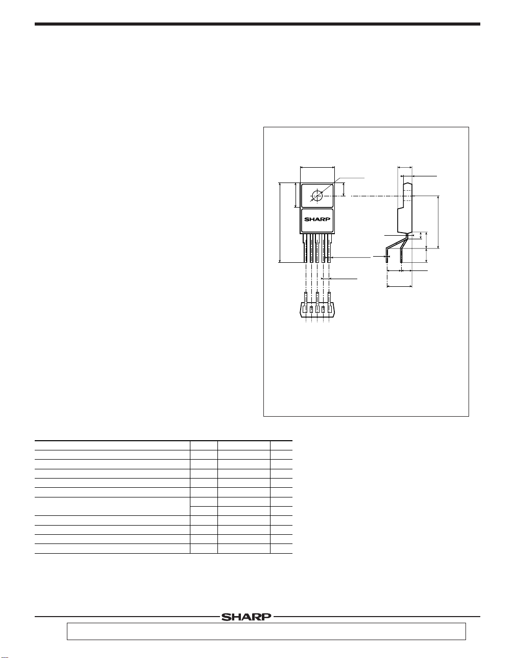
■ Outline Dimensions
10.2MAX
φ3.2±0.1
7.4±0.2
PQ1PF2
(24.6)
●1●2 ●3●4 ●5
3.6±0.2
5-0.8±0.1
4-(1.7)
(Unit : mm)
4.5±0.2
2.8±0.2
(1.5)
(0.5)
(5.0)
8.2±0.7
· ( ) : Typical dimensions
· Radius of lead forming portion
R=TYP 1.0
1 Drain (V
2 GND
3 Control (CA)
4 Feed back (FB)
5 Supply voltage (V
DS)
2.0
3.2±0.5
16.4±0.7
5.0±0.5
4.4MIN
CC)
■ Absolute Maximum Ratings
Drain-GND (source) voltage
Drain current
*1
Power supply voltage
*2
FB terminal input voltage
CA terminal input current
*3
Power dissipation
*4
Junction temperature
Operating temperature
Storage temperature
Soldering temperature
*1
Voltage between V
*2
Voltage between FB-terminal and GND terminal.
*3
P
D1
:No heat sink, PD2:With infinite heat sink
*4
Overheat protection may operate at 125=<T
Parameter Symbol Rating Unit
CC
terminal and GND terminal.
“ In the absence of confirmation by device specification sheets,SHARP takes no responsibility for any defects that may occur in equipment using any SHARP devices
shown in catalogs,data books,etc.Contact SHARP in order to obtain the latest version of the device specification sheets before using any SHARP's device. ”
j
=<150˚C
V
DS
I
D
V
CC
V
FB
I
CA
P
D1
P
D2
T
j
T
opr
T
stg
T
sol
500
3
35
4
2
1.5
18
150
-20 to +80
-40 to +150
260 (For 10s.)
(Ta=25˚C)
V
A
V
V
mA
W
W
˚C
˚C
˚C
˚C
· Please refer to the chapter “ Handling Precautions ”.

Primary Regulators
g
PQ1PF2
■ Electrical Characteristics
Drain-source onstate resistance
Drain-source leakage current
Oscillation frequency
Temperature change in oscillation frequency
Maximum duty
FB threshold voltage
FB current
CA threshold voltage
CA sink current
Overcurrent detecting level
Operation starting voltage
Operation stopping voltage
Stand-by current
Output OFF-mode consumpion current
Output-operating mode consumption current
Charging current
Parameter Symbol Conditions
Fig.1 Test Circuit
C
IN
100µF 0.01µF
A
+
V
CC
V
FB
●5 ●1
PQ1PF2
●4
A
●3
●2
(Unless otherwise specified,conditions shall be VDS=10V,VCC=18V,VCA=OPEN,VFB=2.2V,RL=56Ω, Ta=25˚C)
UnitMAX.TYP.MIN.
R
DS (ON)
I
DSS
fo
∆fo
MAX
D
V
V
V
FB (OCP)
I
V
CAL
V
CAH
V
CA (ON/OFF)
V
CA (OVP)
I
CAIN
I
D (OCP)
V
CC (ON)
V
CC (OFF)
I
CC (ST)
I
CC (OFF)
I
CC (OP)
I
CA (CHG)
FBL
FBH
FB
ID=1.3A
DS
=500V,VCC=7V
V
CA
=GND,VFB=GND
V
j
=0 to 125˚C
T
Duty=0%
MAX
Duty=D
VCA=6V
FB
=GND
V
Duty=0%
MAX
Duty=D
VFB=1V,VCA=6V
DS
=OPEN,VFB=OPEN
V
DS
=OPEN,VFB=OPEN
V
DS
=OPEN,VCC=14V,
V
FB
=OPEN
V
DS
=OPEN,VCA=GND
V
FB
=OPEN
V
CA
=GND,VFB=OPEN
V
-
-
90
-
42
-
-
2.6
-800
-
-
0.49
7.2
20
-
15.5
8.5
-
-
-
-15
2.2
-
100
±5
45
0.9
1.8
2.8
-620
0.9
1.8
0.6
7.7
36
1.8
17.0
9.3
100
0.6
10
-10
3.0
250
110
50
3.1
-440
0.74
8.2
52
18.5
10.1
150
1.8
18
-5
Ω
µA
kHz
-
%
%
-
-
V
V
V
µA
-
-
V
V
V
V
µA
-
A
V
V
µA
mA
mA
µA
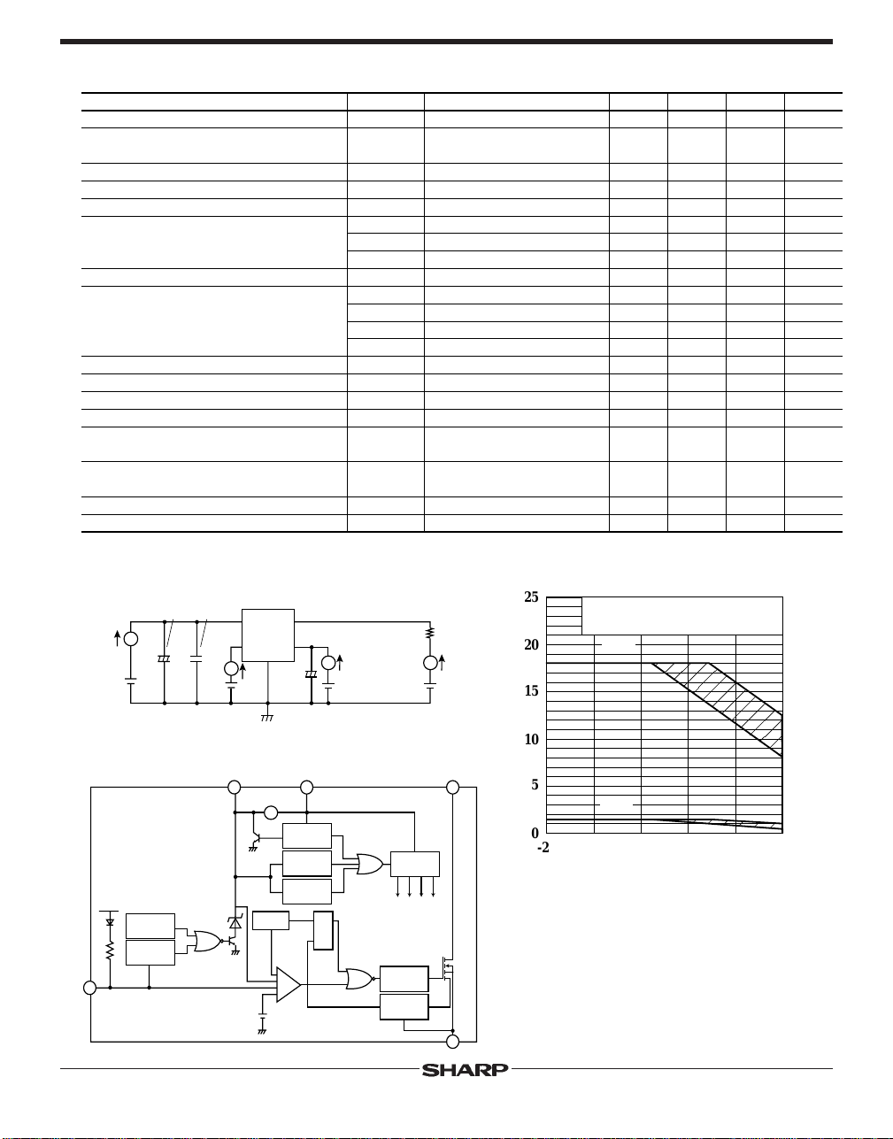
Fig. 2 Power Dissipation vs. Ambient
Temperature
2
R
A A
V
CA
25
R
L
V
DS
(W)
D
20
15
D1
:No heat sink
P
P
D2
:With infinite heat sink
P
D2
■ Block Diagram
V
Constant
voltage
source
GND
DS
1
2
CA V
35
Overheat
detection
circuit
Overload
cut-off voltage
detecting circuit
4
FB
DET
←
O S C
+
-
-
-
CC
Low voltage
malfunction
prevention circuit
Cut-off voltage
detecting circuit
OFF voltage
detecting circuit
R
S
PWM
Q
Drive
circuit
Overcurrent
detecting
circuit
10
Power dissipation P
5
P
D1
0
-200 20406080
Ambient temperature Ta (˚C)
Note) Oblique line portion:Overheat protection may
operate in this area.
 Loading...