Page 1

Chopper Regulators PQ1CF1
PQ1CF1
TO-220 Package Chopper Regulator
■ Features
¡Maximum switching current : 3.5A
¡With ON/OFF control function
¡Built-in oscillation circuit
(oscillation frequency : TYP.70kHz)
¡Built-in overheat protection, overcurrent protection function
¡Variable output voltage (1.26 to 35V /-1.26 to -30V)
[Possible to choose step down output/inversing output according
to external connection circuit]
■ Applications
¡Facsimiles
¡Printers
¡Switching power supplies
¡Personal computers
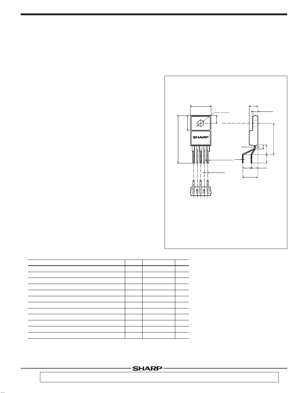
■ Outline Dimensions
10.2MAX
φ3.2±0.1
7.4±0.2
PQ1CF1
(24.6)
5-0.8±0.1
4-(1.7)
●1●2 ●3●4 ●5
3.6±0.2
(1.5)
(0.5)
1 VIN
2 VOUT
3 COM
ADJ
4 O
5 VC
4.5±0.2
(5.0)
8.2±0.7
(Unit : mm)
2.8±0.2
16.4±0.7
2.0
5.0±0.5
4.4MIN
3.2±0.5
■ Absolute Maximum Ratings
*1
Input voltage
Error input voltage
Input-output voltage
*2
Output-COM voltage
*3
ON/OFF control voltage
Switching current terminal voltage
Power dissipation (No heat sink)
Power dissipation (With infinite heat sink)
*4
Junction temperature
Operating temperature
Storage temperature
Soldering temperature
*1
Voltage between V
*2
Voltage between V
*3
Voltage between V
*4
Overheat protection may operate at 125=<T
“ In the absence of confirmation by device specification sheets,SHARP takes no responsibility for any defects that may occur in equipment using any SHARP devices
shown in catalogs,data books,etc.Contact SHARP in order to obtain the latest version of the device specification sheets before using any SHARP's device. ”
Parameter Symbol Rating Unit
V
IN
V
ADJ
Vi-o
OUT
V
V
C
SW
D1
D2
T
j
opr
stg
sol
-0.3 to 40
-20 to +80
-40 to +150
260 (For 10s)
IN
terminal and COM terminal.
OUT
terminal and COM terminal.
C
terminal and COM terminal.
j
=<150˚C
I
P
P
T
T
T
(Ta=25˚C)
40
7
41
-1
V
V
V
V
V
3.5
1.5
15
150
A
W
W
˚C
˚C
˚C
˚C
· Please refer to the chapter“ Handling Precautions ”.
Page 2

Chopper Regulators PQ1CF1
■ Electrical Characteristics
Parameter Symbol Conditions UnitMAX.TYP.MIN.
Output saturation voltage
Reference voltage
Temperature coefficient in reference voltage
Load regulation
Line regulation
Efficiency
Oscillation frequency
Oscillation frequency temperature fluctuation
Maximum duty
Overcurrent detecting level
Charge current1
Charge current2
Input threshold voltage
On threshold voltage
Stand-by current
Output OFF-state consumption current
■ Block Diagram
1 V
IN
Voltage
regulator
circuit
PWM COMP.
Overcurrent
detecting
circuit
Overheat
detecting
circuit
F/F
Q
R
S
(Unless otherwise specified, conditions shall be VIN=12V, Io=0.5A, VO=5V, Ta=25˚C)
I
SW=
V
SAT
V
ref
∆V
ref
|RegL|
eg
I|
|R
η
fo
∆fo
MAX
D
I
L
I
CHG1
I
CHG2
V
THL
V
THH
VTH(ON)
SD
I
I
qS
ON/OFF
circuit
+
-
Oscillator
3A
-
j
=0 to 125˚C
T
O
=0.5 to 3A
I
IN
=8 to 35V
V
O
=3A
I
-
j
=0 to 125˚C
T
4terminal is open
-
24terminal is open, 5terminal
24terminal is open, 5terminal=0.7V
Duty
=0%, 4terminal=0V, 5terminal
Duty=D
MAX
, 4terminal is open,5terminal
4terminal=0V, 5terminal
IN
=40V, 5terminal=0V
V
IN
=40V, 5terminal=0.7V
V
2 V
OUT
↓
Soft start
4 O
ERROR AMP.
+
-
V
ref
ADJ
-
1.235
-
-
-
-
60
-
90
3.9
-50
-150
0.75
1.55
0.5
-
-
1.4
1.26
±0.6
0.2
0.6
80
70
±5
-
5.1
-30
-100
0.9
1.8
0.6
140
8
1.8
1.285
-
1.5
2.5
-
80
-
-
6.3
-10
-50
1.2
2.05
0.7
400
16
V
V
%
%
%
%
kHz
%
%
A
µA
µA
V
V
V
µA
mA
Fig.1 Test Circuit
IN
C
220µF
●4
●1 ●2
PQ1CF1
●3
0.068µF
I
SD
I
QS
A
V
IN
3 COM
L
90µH
R
●5
5.1kΩ
L : HK-12S120-9000R (made by Toho Co.)
D : ERC80-004 (made by Fuji electronics Co.)
2
D
R
1
1kΩ
I
++
C
O
1000µF
5 V
O
C
V
Fig.2 Power Dissipation vs. Ambient
Temperature
20
15
(W)
O
Load
D
10
5
Power dissipation P
0
-20 0 20 40 60 10080
protection may operate in this area.
D1
:No heat sink
P
P
D2
:With infinite heat sink
D2
P
P
D1
Ambient temperature Ta (˚C)
Note) Oblique line portion : Overheat
Page 3

Chopper Regulators PQ1CF1
■ Step Down Type Circuit Diagram (5V output)
V
IN
8 to 35V
IN
C
220µF
●4
●1 ●2
PQ1CF1
●3
R
5.1kΩ
C
C
0.068µF
●5
C
D
L
90µH
R
3kΩ
R
1kΩ
V
O
=5V
2
++
C
1
O
1000µF
Load
ON/OFF control
■ Polarity Inversion Type Circuit Diagram (-5V output)
L
65µH
R
3kΩ
D
R
1kΩ
ON/OFF control
2
++
C
1
O
2200µF
Load
VO=-5V
VIN
5 to 30V
IN
C
220µF
●4
●1 ●2
PQ1CF1
●3
R
5.1kΩ
C
C
0.068µF
●5
C
 Loading...