

Datasheet PQ015EH01ZP, PQ018EH01ZZ, PQ018EH01ZP, PQ025EH01ZZ, PQ025EH01ZP Datasheet (SHARP)
...
Low Power-Loss Voltage Regulators PQxxxEH01Z Series
查询PQ015EH01ZP供应商
PQxxxEH01Z Series
Low Voltage Operation Low Power-Loss Voltage Regulators
Features
■
●
Low voltage operation (Minimum operating voltage: 2.35V)
2.5V input → available 1.5 to 1.8V output
●
Large output current type (IO: 1A)
●
Low dissipation current
(Dissipation current at no load: MAX. 2mA
Output OFF-state dissipation current: MAX.5µA)
●
Low power-loss
●
Built-in overcurrent and overheat protection functions
●
TO-263 package
Applications
■
●
Peripheral equipment of personal computers
●
Power supplies for various electronic equipment such as
DVD player or STB
Model Line-up
■
Output
current (IO)
1A
Package
type
Taping
Sleeve
PQ015EH01ZP
PQ015EH01ZZ
Output voltage (VO)
1.8V1.5V 2.5V
PQ018EH01ZP
PQ018EH01ZZ
PQ025EH01ZP
PQ025EH01ZZ
Outline Dimensions
■
MAX.
10.6
±0.5
3.28
(0.55)
015EH01
±0.5
MAX.
8.4
13.7
(0.6) (0.6)
(0.45)
+0.2
1.05
–0.1
+0.2
3–0.9
–0.1
1
1
Specific IC
1
DC input (V
2
ON/OFF control terminal (V
3
DC output (VO)
4
NC
5
GND
6
DC output (VO)
( ) : Typical dimensions
5
IN)
(0.45)
4–(1.7)
5432
ø2
1.05
3
2
6
Epoxy resin
+0.2
–0.1
C)
3.5
(0.6)
±0.5
(Unit : mm)
(0.6)
(2.4)( 1.3)
0 to 0.25
Absolute Maximum Ratings
■
Parameter Symbol Rating Unit
Input voltage
❇1
ON/OFF control terminal voltage
Output current
❇2
Power dissipation
❇3
Junction temperature
Operating temperature
Storage temperature
Soldering temperature
❇1 All are open except GND and applicable terminals.
:With infinite heat sink
❇2 P
D
❇3 Overheat protection may operate at T
Notice In the absence of confirmation by device specification sheets,SHARP takes no responsibility for any defects that may occur in equipment using any SHARP
devices shown in catalogs,data books,etc.Contact SHARP in order to obtain the latest device specification sheets before using any SHARP device.
Internet Internet address for Electronic Components Group http://sharp-world.com/ecg/
IN
V
V
C
O
I
D
T
j
T
opr
T
stg
T
sol
=125˚C to 150˚C.
j
(Ta=25°C)
10
10
1
35 WP
150
−40 to +85
˚C
˚C
−40 to +150 ˚C
260 (10s) ˚C
V
V
A
•Please refer to the chapter " Handling Precautions ".

Low Power-Loss Voltage Regulators PQxxxEH01Z Series
Electrical Characteristics
■
Parameter Symbol Conditions
Input voltage
Output voltage
Load regulation
Line regulation
Temperature coefficient of output voltage
Ripple rejection
❇4
ON-state voltage for control
ON-state current for control
OFF-state voltage for control
OFF-state current for control
Quiescent current
Output OFF-state dissipation current
❇4 In case of opening control terminal , output voltage turns off
Input Voltage Line-up
■
Model No. Symbol Conditions
PQ015EH01Z
PQ018EH01Z
PQ025EH01Z
2
V
IN
V
IN
V
IN
(Unless otherwise specified, condition shall be VIN=VO(TYP)+1V, IO=0.5A, VC
MIN.
VIN
VO
RegL
R
egI
VIN=VO(TYP)+1V to VO(TYP)+6V, IO=5mA
T
CVO
Tj=0 to 125˚C, IO=5mA
RR
V
C (ON)
IC (ON)
VC (OFF)
IC (OFF)
Iq
Iqs
−
−
I
O=5mA to 1A
Refer to Fig.2
−
−
−
C=0.4V
V
IO=0A
O=0A, VC=0.4V
I
Refer to below table
Refer to below table
−
0.2
−
0.1
−−
±0.01
45
60
2
−
−
−
−
−
−
−
−
1mA
−
−
MIN.
2.35 − 10 V
I
O
=0.5A, VC=2.7V, Ta=25˚C
2.35 − 10
3
− 10
=2.7V, Ta=25˚C)
MAX.TYP.
Unit
V
V
2.0
1.0
%
%
%/˚C
−
dB
−
V
200
µA
0.8
V
µA
2
2
µA
5
MAX.TYP.
Unit
V
V
Output Voltage Line-up
■
Model No. Symbol Conditions
PQ015EH01Z
PQ018EH01Z
PQ025EH01Z
Fig.1 Test Circuit
V
IN
0.33µF
MIN.
V
O
V
O
V
O
V
IN=VO
(TYP)+1V, IO=0.5A, VC=2.7A, Ta=25˚C
1
5
A
3
2
I
q
V
C
I
A
C
1.45 1.5 1.55 V
1.75 1.8 1.85
2.438
+
47µF
MAX.TYP.
2.5 2.562
I
A
O
R
L
Unit
V
V
V
O
V

Low Power-Loss Voltage Regulators PQxxxEH01Z Series
Fig.2 Test Circuit for Ripple Rejection
1
ei
~
V
IN
0.33µF
5
Fig.3 Power Dissipation vs. Ambient
Temperature
40
PD : With infinite heat sink
35
30
(W)
D
25
20
15
Power dissipation P
10
5
0
−40 −200 20406080100
Note) Oblique line portion:Overheat protection may operate in this area.
Fig.5
Ambient temperature Ta (°C)
Overcurrent Protection Characteristics
(Typical Value, PQ018EH01Z)
1.8
1.6
1.4
(V)
1.2
O
1
0.8
0.6
Output voltage V
0.4
0.2
0
0 0.5 1 1.5 2
VIN=2.35V
VIN=2.5V
VIN=3V
VIN=3.3V
VIN=5V
Output current IO (A)
3
V
C
2
2.7V
Fig.4
+
47µF
f=120Hz(sine wave)
ei(rms)=0.5V
V
(TYP)+2V
IN=VO
=0.3A
I
O
RR=20log(ei(rms)/eo(rms))
Overcurrent Protection Characteristics
+
I
O
R
L
eo
V
~
(Typical Value, PQ015EH01Z)
1.5
1.2
(V)
O
0.9
0.6
Output voltage V
0.3
0
0 0.5 1 1.5 2
Fig.6
Overcurrent Protection Characteristics
VIN=2.35V
VIN=2.5V
VIN=3V
VIN=3.3V
VIN=5V
Output current IO (A)
(Typical Value, PQ025EH01Z)
2.5
2
(V)
O
1.5
1
Output voltage V
0.5
0
0 0.5 1 1.5 2
VIN=3V
VIN=3.3V
VIN=3.6V
VIN=4.5V
VIN=5V
Output current IO (A)

Low Power-Loss Voltage Regulators PQxxxEH01Z Series
Output voltage V
O
(V)
1.75
1.76
1.77
1.78
1.79
1.8
1.81
1.82
1.83
1.84
1.85
−50 −25 0 25 50 75 100 125
Ambient temperature T
a
(°C)
VIN=2.8V
I
O
=0.5A
V
C
=2.7V
Fig.7 Output Voltage vs. Ambient
Temperature (PQ015EH01Z)
(V)
O
1.55
1.54
1.53
1.52
1.51
VIN=2.5V
=0.5A
I
O
=2.7V
V
C
1.5
1.49
1.48
Output voltage V
1.47
1.46
1.45
−50 −25 0 25 50 75 100 125
Ambient temperature T
(°C)
a
Fig.9 Output Voltage vs. Ambient
Temperature (PQ025EH01Z)
2.525
2.52
2.515
2.51
(V)
O
2.505
2.5
2.495
2.49
Output voltage V
2.485
2.48
2.475
−50 −25 0 25 50 75 100 125
Ambient temperature T
(°C)
a
VIN=3.5V
=0.5A
I
O
=2.7V
V
C
Fig.8 Output Voltage vs. Ambient
Temperature (PQ018EH01Z)
Fig.10 Output Voltage vs. Input Voltage
(PQ015EH01Z)
1.6
1.4
1.2
(V)
O
1
0.8
0.6
Output voltage V
0.4
0.2
0
012345
RL=1.5Ω (IO=1A)
RL=3Ω (IO=0.5A)
RL=∞Ω (IO=0A)
Input voltage V
VC=2.7V
=Room temp.
T
a
C
IN
C
O
(V)
IN
=0.33µF
=47µF
Fig.11 Output Voltage vs. Input Voltage
(PQ018EH01Z)
2
1.8
1.6
1.4
(V)
O
1.2
1
0.8
Output voltage V
0.6
0.4
0.2
0
012345
Input voltage V
RL=1.8Ω (IO=1A)
RL=3.6Ω (IO=0.5A)
RL=∞Ω (IO=0A)
VC=2.7V
=Room temp.
T
a
C
IN
C
O
(V)
IN
=0.33µF
=47µF
Fig.12 Output Voltage vs. Input Voltage
(PQ025EH01Z)
2.5
2
(V)
O
1.5
1
Output voltage V
0.5
0
012345
Input voltage V
RL=2.5Ω (IO=1A)
RL=5Ω (IO=0.5A)
RL=0Ω (IO=0A)
VC=2.7V
=Room temp.
T
a
=0.33µF
C
IN
=47µF
C
O
(V)
IN

Low Power-Loss Voltage Regulators PQxxxEH01Z Series
j
Ripple rejection RR (dB)
0.1 1 10 100
Input ripple frequency f (kHz)
35
40
45
50
55
60
65
70
75
ei (rms) =0.5V
V
C
=2.7V
I
O
=0.3A
C
O
=47µF
Ta=Room temp.
PQ025EH01Z (VIN=4.5V)
PQ018EH01Z (VIN=3.8V)
PQ015EH01Z (VIN=3.5V)
Fig.13 Circuit Operating Current vs. Input
Voltage (PQ015EH01Z)
20
(mA)
BIAS
10
Circuit operating current I
0
012345
Input voltage V
VC=2.7V
=Room temp.
T
a
=0.33µF
C
IN
=10µF
C
O
RL=1.5Ω (IO=1A)
RL=3Ω (IO=0.5A)
RL=∞Ω (IO=0A)
(V)
IN
Fig.15 Circuit Operating Current vs. Input
Voltage (PQ025EH01Z)
30
(mA)
BIAS
20
10
Circuit operating current I
0
012345
Input voltage V
VC=2.7V
=Room temp.
T
a
=0.33µF
C
IN
=47µF
C
O
RL=2.5Ω (IO=1A)
RL=5Ω (IO=0.5A)
RL=∞Ω (IO=0A)
(V)
IN
Fig.14 Circuit Operating Current vs. Input
Voltage (PQ018EH01Z)
20
(mA)
BIAS
10
Circuit operating current I
0
012345
Input voltage V
VC=2.7V
=Room temp.
T
a
=0.33µF
C
IN
=47µF
C
O
RL=1.8Ω (IO=1A)
RL=3.6Ω (IO=0.5A)
RL=∞Ω (IO=0A)
(V)
IN
Fig.16 Quiescent Current vs. Junction
Temperature
1.4
PQ025EH01Z:VIN=3.5V
1.2
1
(mA)
q
0.8
0.6
0.4
Quiescent current I
0.2
PQ018EH01Z:VIN=2.8V
0
−50 −25 0 25 50 75 100 125
Junction temperature T
PQ015EH01Z:VIN=2.5V
(°C)
IO=0A
=2.7V
V
C
Fig.17
ON-OFF Threshold Voltage vs. Ambient
Temperature (PQ018EH01Z)
2.5
(V)
2
TH (ON/OFF)
1.5
1
0.5
ON-OFF threshold voltage V
0
−50 −25 0 25 50 75 100 125
Ambient temperature T
Fig.18 Ripple Rejection vs. Input Ripple
Frequency
VIN=2.5V
=0A
I
O
(°C)
a
Low Power-Loss Voltage Regulators PQxxxEH01Z Series
Material : Glass-cloth epoxy resin
Size : 60×60×1.6mm
Cu thickness : 65µm
PWB
PWB
Cu
Fig.19 Ripple Rejection vs. Output Current
80
75
70
65
PQ025EH01Z (VIN=4.5V)
60
55
Ripple rejection RR (dB)
50
45
40
0 0.25 0.5 0.75 1
Fig.20 Power Dissipation vs. Ambient
Temperature (Typical Value)
6
PQ015EH01Z (VIN=3.5V)
PQ018EH01Z (VIN=3.8V)
ei (rms) =0.5V
f=120Hz
=2.7V
V
C
=47µF
C
O
Ta=Room temp.
Output current IO (A)
(W)
D
5
Cu area 3 600mm
4
Cu area 900mm
3
Cu area 400mm
Cu area 115mm
2
2
2
2
2
Power dissipation P
1
0
−40 −200 20406080
Ambient temperature T
a
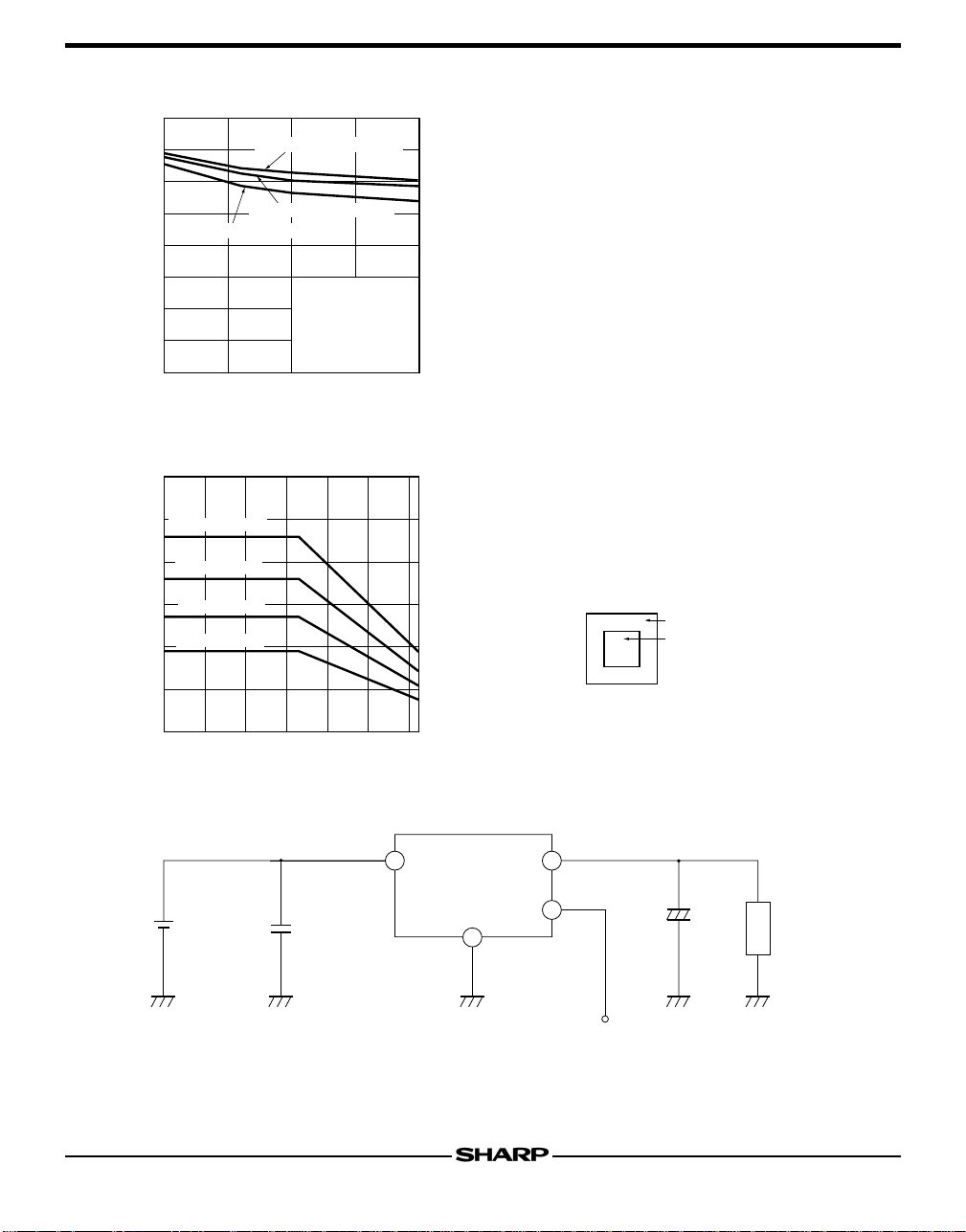
Fig.21 Typical Application
V
IN
C
IN
(°C)
1 3
V
O
2
5
ON/OFF signal
CO+
High:Output ON
Low or open:Output OFF
Load

NOTICE
●
The circuit application examples in this publication are provided to explain representative applications of SHARP
devices and are not intended to guarantee any circuit design or license any intellectual property rights. SHARP takes
no responsibility for any problems related to any intellectual property right of a third party resulting from the use of
SHARP's devices.
●
Contact SHARP in order to obtain the latest device specification sheets before using any SHARP device. SHARP
reserves the right to make changes in the specifications, characteristics, data, materials, structure, and other contents
described herein at any time without notice in order to improve design or reliability. Manufacturing locations are
also subject to change without notice.
●
Observe the following points when using any devices in this publication. SHARP takes no responsibility for damage
caused by improper use of the devices which does not meet the conditions and absolute maximum ratings to be used
specified in the relevant specification sheet nor meet the following conditions:
(i) The devices in this publication are designed for use in general electronic equipment designs such as:
--- Personal computers
--- Office automation equipment
--- Telecommunication equipment [terminal]
--- Test and measurement equipment
--- Industrial control
--- Audio visual equipment
--- Consumer electronics
(ii) Measures such as fail-safe function and redundant design should be taken to ensure reliability and safety when
SHARP devices are used for or in connection with equipment that requires higher reliability such as:
--- Transportation control and safety equipment (i.e., aircraft, trains, automobiles, etc.)
--- Traffic signals
--- Gas leakage sensor breakers
--- Alarm equipment
--- Various safety devices, etc.
(iii)SHARP devices shall not be used for or in connection with equipment that requires an extremely high level of
reliability and safety such as:
--- Space applications
--- Telecommunication equipment [trunk lines]
--- Nuclear power control equipment
--- Medical and other life support equipment (e.g., scuba).
●
Contact a SHARP representative in advance when intending to use SHARP devices for any "specific" applications
other than those recommended by SHARP or when it is unclear which category mentioned above controls the
intended use.
●
If the SHARP devices listed in this publication fall within the scope of strategic products described in the Foreign
Exchange and Foreign Trade Control Law of Japan, it is necessary to obtain approval to export such SHARP devices.
●
This publication is the proprietary product of SHARP and is copyrighted, with all rights reserved. Under the copyright
laws, no part of this publication may be reproduced or transmitted in any form or by any means, electronic or
mechanical, for any purpose, in whole or in part, without the express written permission of SHARP. Express written
permission is also required before any use of this publication may be made by a third party.
●
Contact and consult with a SHARP representative if there are any questions about the contents of this publication.
 Loading...