

Page 1

SERVICE MANUAL
■ LEAD-FREE SOLDER
MODEL
CONTENTS
CODE : 00Z
PN525USM/E
LCD MONITOR
PN-525U
CHAPTER 1. OUTLINE OF THE PRODUCT,
NOMENCLATURE AND FUNCTION . . . . . . . . . . . .1 - 1
CHAPTER 2. CONNECTION, ADJUSTMENT,
OPERATION, AND FUNCTION . . . . . . . . . . . . . . . .2 - 1
CHAPTER 3. DISASSEMBLY AND ASSEMBLY . . . . . . . . . . . . . .3 - 1
CHAPTER 4. BLOCK DIAGRAM . . . . . . . . . . . . . . . . . . . . . . . . . .4 - 1
CHAPTER 5. TROUBLESHOOTING . . . . . . . . . . . . . . . . . . . . . . .5 - 1
CHAPTER 6. HARDWARE DESCRIPTIONS. . . . . . . . . . . . . . . . .6 - 1
CHAPTER 7. CIRCUIT DIAGRAM & PARTS LAYOUT . . . . . . . . .7 - 1
Parts marked with "!" are important for maintaining the safety of the set. Be sure to replace these parts with specified
ones for maintaining the safety and performance of the set.
This document has been published to be used
for after sales service only.
The contents are subject to change without notice.
Page 2
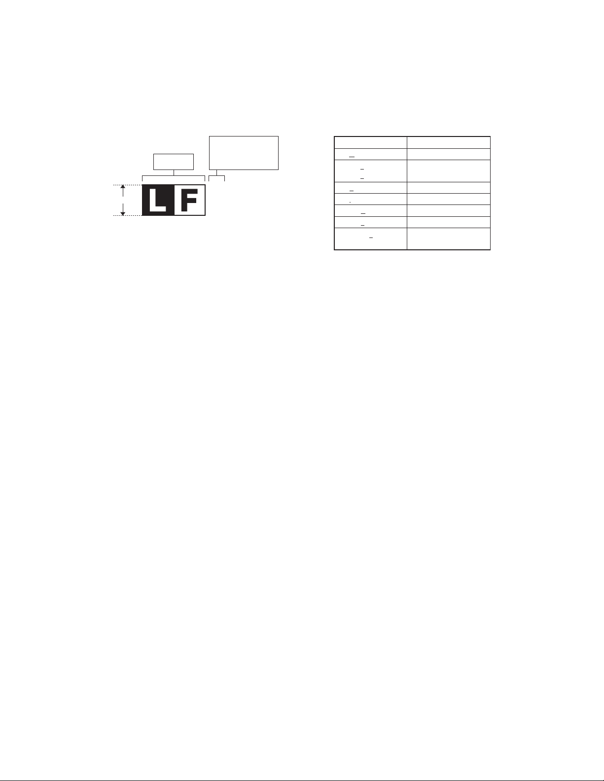
■ LEAD-FREE SOLDER
The PWB’ s of this model employs lead-free solder. The “LF” marks indicated on the PWB’s and the Service Manual mean “Lead-Free” solder. The
alphabet following the LF mark shows the kind of lead-free solder.
Example:
<Solder composition code of lead-free solder>
Solder composition
Sn-Ag-Cu
Sn-Ag-Bi
Sn-Ag-Bi-Cu
Sn-Zn-Bi
Sn-In-Ag-Bi
Sn-Cu-Ni
Sn-Ag-Sb
Bi-Sn-Ag-P
Bi-Sn-Ag
5mm
Lead-Free
Solder composition
code (Refer to the
table at the right.)
a
(1) NOTE FOR THE USE OF LEAD-FREE SOLDER THREAD
When repairing a lead-free solder PWB, use lead-free solder thread. Never use conventional lead solder thread, which may cause a breakdown or an
accident.
Since the melting point of lead-free solder thread is about 40°C higher than that of conventional lead solder thread, the use of the exclusive-use soldering iron is recommendable.
Solder composition code
a
b
z
i
n
s
p
(2) NOTE FOR SOLDERING WORK
Since the melting point of lead-free solder is about 220°C, which is about 40°C higher than that of conventional lead solder, and its soldering capacity
is inferior to conventional one, it is apt to keep the soldering iron in contact with the PWB for longer time. This may cause land separation or may
exceed the heat-resistive temperature of components. Use enough care to separate the soldering iron from the PWB when completion of soldering is
confirmed.
Since lead-free solder includes a greater quantity of tin, the iron tip may corrode easily. Turn ON/OFF the soldering iron power frequently.
If different-kind solder remains on the soldering iron tip, it is melted together with lead-free solder. To avoid this, clean the soldering iron tip after completion of soldering work.
If the soldering iron tip is discolored black during soldering work, clean
and file the tip with steel wool or a fine filer.
PN-525U LEAD-FREE SOLDER
Page 3
CHAPTER 1. OUTLINE OF THE PRODUCT, NOMENCLATURE AND FUNCTION
1. SPECIFICATIONS
Model PN-525U
LCD element 52” wide (132.2 cm diagonal)
Max. resolution
(pixels)
Max. colors 16.77 M colors (8 bits/color)
Pixel pitch 0.600mm (H)
Viewing angle 176° right/left/up/down (contrast ratio >
Screen active
area inch (mm)
Computer input
signal
Sync
signal
Video signal
system
Plug and play VESA DDC2B
Power
management
Input terminals PC/AV Digital DVI-D 24 pin
Output terminals PC/AV Digital DVI-D 24 pin
Power
requirement
Operating
temperature
Operating
humidity
Power
consumption
Dimensions
inch (mm)
Weight lbs. (kg) Approx. 97.0 (44)
*1 Cannot be used simultaneously.
*2 Does not support plug and play.
*3 Connection is allowed with an HDCP-compatible device only.
Does not support Repeater control function.
*4 When AUTO INPUT CHANGE is OFF. 11.5 W when it is ON.
ASV low-reflection black TFT LCD
× 1080
1920
× 0.600mm (V)
45-3/8
× 25-1/2 (1152.0 × 648.0)
Digital (DVI 1.0 standard-compliant),
Analog RGB (0.7Vp-p) [75Ω]
Horizontal/vertical separate
(TTL: positive/negative), Sync-on-green,
Composite sync (TTL: positive/negative)
PAL, PAL-60, SECAM, NTSC (3.58MHz),
NTSC (4.43MHz)
VESA DPMS, DVI DMPM
(HDCP compatible)
PC Analog Mini D-sub 15 pin,
× 1, BNC
3 rows
Audio 3.5 mm mini stereo jack
AV Composite
BNC
× 1
video
Component
BNC (Y, Cb/Pb, Cr/Pr)
Audio RCA pin (L/R) × 1
Serial (RS-232C) D-sub 9 pin
× 1
× 1
Audio RCA pin (L/R) × 1
Serial (RS-232C) D-sub 9 pin
Speaker 7W
AC 120 V, 60 Hz
32°F to 104°F (0°C to 40°C)
20% to 80% (no condensation)
325W (Input signal waiting mode: 7.5W
Standby mode: 3.5W)
Approx. 49-3/8
(1,254
×5-7/8 ×29-3/16.
× 149 ×742) (excluding protrusions)
(excluding the temporarystand)
× 1
+ 7W [6Ω]
10)
*3
*1*2
*
1
× 1
,
× 1
*
1
× 1
× 1
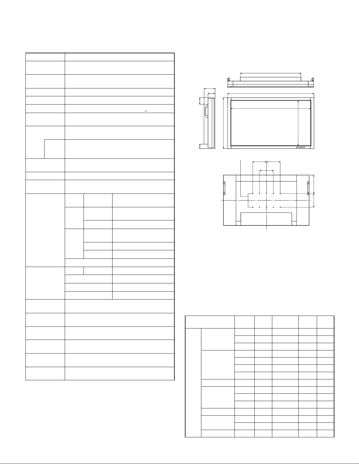
■ DIMENSIONAL DRAWINGS
Note: That the values shown are approximate values.
Unit: inch [mm]
34-3/4 [882]
5-7/8 [149]
3-5/8
[92]
3-3/4 [95] 2-5/8 [66]
Opening width (45-9/16 [1157])
29-3/16 [742]
VESA holes
49-3/8 [1254]
7-7/8
[200]
7-7/8 [200]
7-7/8
[200]
Opening height
(25-11/16 [653])
[271]
10-11/16
[200]
7-7/8
When mounting the monitor, be sure to use a wall-mount / ceilingmount bracket they comply with the VESA-compatible mounting
method. SHARP recommends using M6 screws and tighten the screws.
Note that screw hole depth of the monitor is 3/8 inch (10 mm). Loose
holding may cause the product to fall, resulting in serious personal injuries as well as damage to the product. The screw and hole should come
together with over 5/16 inch (8 mm) length of thread. Use the bracket
which applied UL1678 standard, and which can endure at least 4 times
or more the weight of the monitor.
■ COMPATIBLE SIGNAL TIMING (PC)
Screen resolution Hsync Vsync
VESA 640
× 480 31.5kHz 60Hz 25.175MHz oo
37.9kHz 72Hz 31.5MHz oo
37.5kHz 75Hz 31.5MHz oo
× 600 35.1kHz 56Hz 36.0MHz o
800
37.9kHz 60Hz 40.0MHz oo
48.1kHz 72Hz 50.0MHz oo
46.9kHz 75Hz 49.5MHz oo
× 480 31.0kHz 60Hz 33.75MHz oo
848
1024
× 768 48.4kHz 60Hz 65.0MHz oo
56.5kHz 70Hz 75.0MHz oo
60.0kHz 75Hz 78.75MHz oo
× 864 67.5kHz 75Hz 108.0MHz oo
1152
1280
× 768 47.8kHz 60Hz 79.5MHz oo
60.3kHz 75Hz 102.25MHz oo
× 960 60.0kHz 60Hz 108.0MHz oo
1280
Dot
frequency
Analog
signal
Digital
signal
-
PN-525U OUTLINE OF THE PRODUCT, NOMENCLATURE AND FUNCTION
1 – 1
Page 4
Screen resolution Hsync Vsync
VESA
Wide 1280
US
TEXT
Sun 1024
*1 Displays a reduced image.
* All are compliant only with non-interlaced.
* Depending on the connected PC, images may not be displayed
properly even if the compatible signal described above is input.
* The frequency values for the Sun are reference values.
× 1024 64.0kHz 60Hz 108.0MHz oo
1280
80.0kHz 75Hz 135.0MHz oo
1360
× 768 47.7kHz 60Hz 85.5MHz oo
*
1600 × 1200
1
75.0kHz 60Hz 162.0MHz oo
× 720 44.7kHz 60Hz 74.4MHz oo
1920
× 1080 66.3kHz 60Hz 148.5MHz oo
× 400 31.5kHz 70Hz 28.3MHz oo
720
× 768 48.3kHz 60Hz 64.13MHz o
53.6kHz 66Hz 70.4MHz o
56.6kHz 70Hz 74.25MHz o
1152 × 900 61.8kHz 66Hz 94.88MHz o
71.8kHz 76.2Hz 108.23MHz o
1280 × 1024 71.7kHz 67.2Hz 117.01MHz o
81.1kHz 76Hz 134.99MHz o
1600 × 1000 68.6kHz 66Hz 135.76MHz o
Dot
frequency
Analog
signal
Digital
signal
-
-
-
-
-
-
-
-
■ PC1/AV1 INPUT TERMINAL PINS
(DVI-D 24 Pin)
No. Function No. Function
1 TMDS data 2- 13 N.C.
2 TMDS data 2
3 TMDS data 2/4 shield 15 GND
4 N.C. 16 Hot-plug detection
5 N.C. 17 TMDS data 0
6 DDC clock 18 TMDS data 0+
7 DDC data 19 TMDS data 0/5 shield
8N.C. 20N.C.
9 TMDS data 1
10 TMDS data 1
11 TMDS data 1/3 shield 23 TMDS clock
12 N.C. 24 TMDS clock−
+ 14 +5V
−
− 21 N.C.
+ 22 TMDS clock shield
+
■ RS-232C INPUT TERMINAL PINS
(D-sub 9 Pin)
No. Function No. Function
1N.C. 6N.C.
2 Transmitted data 7 N.C.
3 Received data 8 N.C.
4N.C. 9N.C.
5GND
■ RS-232C OUTPUT TERMINAL PINS
(D-sub 9 Pin)
No. Function No. Function
1N.C. 6N.C.
2 Received data 7 N.C.
3 Transmitted data 8 N.C.
4N.C. 9N.C.
5GND
■ PC2 RGB INPUT TERMINAL PINS
(Mini D-sub 15 Pin)
No. Function No. Function
1 Red video signal input 9
2 Green video signal input 10 GND
3 Blue video signal input 11 N.C.
4 N.C. 12 DDC data
5 GND 13 Hsync signal input
6 GND for red video signal 14 Vsync signal input
7 GND for green video signal 15 DDC clock
8 GND for blue video signal
+5V
■ PC/AV OUTPUT TERMINAL PINS
(DVI-D 24 Pin)
No. Function No. Function
1TMDS data 2
2TMDS data 2
3 TMDS data 2/4 shield 15 GND
4 N.C. 16 Hot-plug detection
5 N.C. 17 TMDS data 0
6 DDC clock 18 TMDS data 0+
7 DDC data 19 TMDS data 0/5 shield
8N.C. 20N.C.
9TMDS data 1
10 TMDS data 1
11 TMDS data 1/3 shield 23 TMDS clock
12 N.C. 24 TMDS clock−
− 13 N.C.
+ 14 +5V
− 21 N.C.
+ 22 TMDS clock shield
+
−
PN-525U OUTLINE OF THE PRODUCT, NOMENCLATURE AND FUNCTION
1 – 2
Page 5
■ POWER MANAGEMENT
ŊŏőŖŕ
This monitor conforms to VESA DPMS and DVI DMPM. Both your video
card and computer must support the same standard in order for the
monitor’s power management function to work.
DPMS: Display Power Management Signaling
DPMS Screen
Power
consumption
Hsync Vsync
ON STATE Display 325W Yes Yes
STANDBY
SUSPEND Yes No
OFF STATE No No
No
display
7.5W
No Yes
DMPM: Digital Monitor Power Management
DMPM Screen
Power
consumption
Monitor ON Display 325W
Active OFF
No
display
7.5W
*When AUTO INPUT CHANGE is OFF. 11.5 W when it is ON.
■ DDC (PLUG AND PLAY)
The monitor supports the VESA DDC (Display Data Channel) standard.
DDC is a signal standard for plug and play between monitors and computers. Information about resolution and other parameters is exchanged
between the two. This function can be used if the computer supports
DDC and it has been configured to detect plug-and-play monitors.
There are several types of DDC, depending on the communication
method used. This monitor supports DDC2B.
2. SUPPLIED ACCESSORIES
Liquid Crystal Display: 1
*Sharp Corporation holds authorship rights to the Utility Disk program.
Do not reproduce it without permission.
*For environmental protection!
Do not dispose of batteries in household waste. Follow the disposal
instructions for your area.
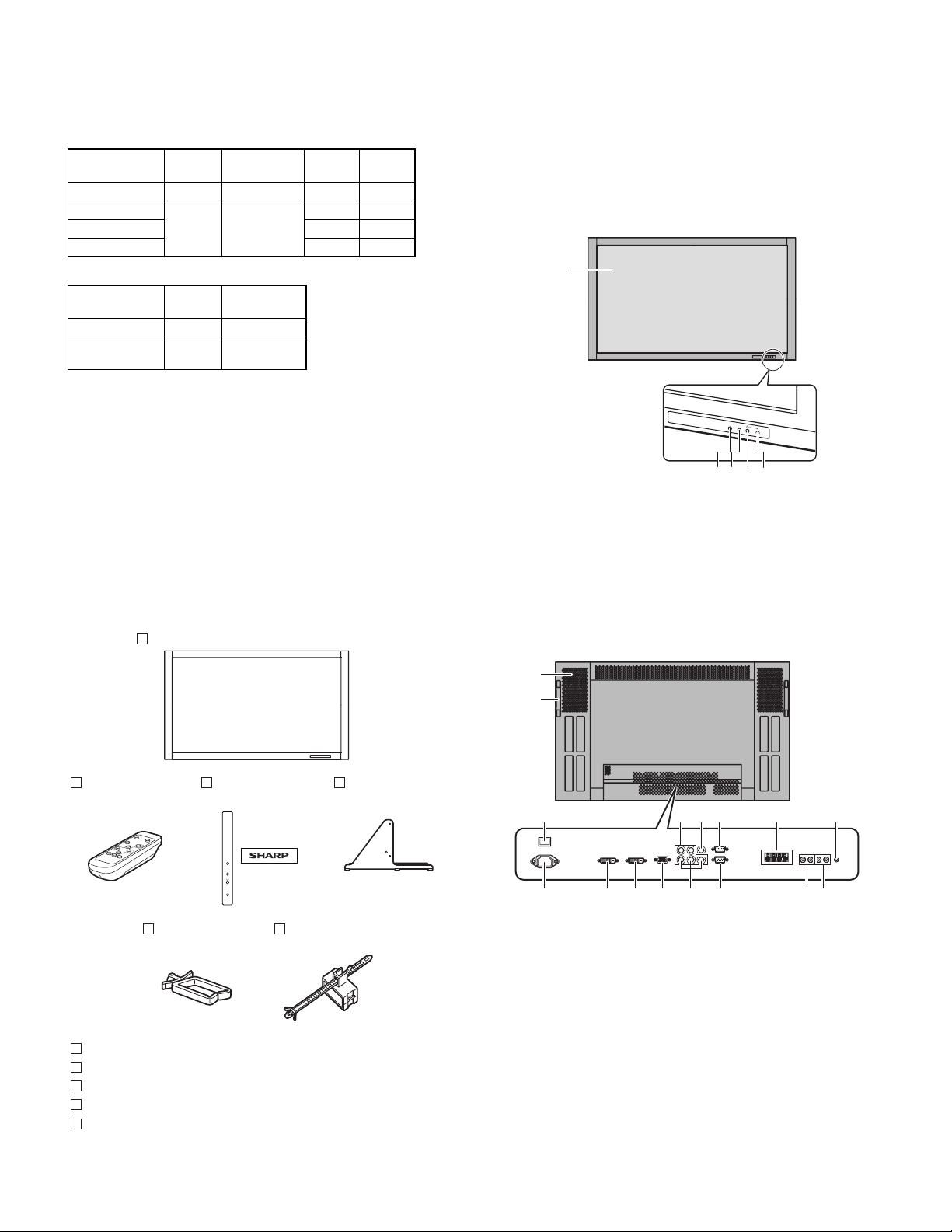
3. PART NAMES AND FUNCTION
■ FRONT VIEW
1
2345
*Use a pointed object such as a pen tip to press the switches at the
front of the monitor.
1 LCD panel
2 Remote control sensor
3 Input switch
4 Power switch
5 Power LED
■ REAR VIEW
Remote control
unit: 1
Cable clamp: 2
Vertical logo
sticker: 2
INPUT
Power cord
Temporary stand: 2
clamp: 1
Power cord (Approx. 13.1 feet [4 m]): 1
“AA” size battery: 2
CD-ROM (Utility Disk for Windows): 1
Operation manual: 1
Blank sticker: 1
Place a blank sticker onto the SHARP logo to cover the logo.
L
K
1689
GJ
H
I23457F
1 Main power switch 9 RS-232C output terminal
(D-sub 9 pin)
2 AC input terminal F RS-232C input terminal
(D-sub 9 pin)
3 PC/AV output terminal (DVI-D) G External speaker terminals
4 PC1 input terminal (DVI-D) H PC/AV audio output terminals
AV1 input terminal (DVI-D) I AV audio input terminals
5 PC2 input terminal
J PC audio input terminal
(Mini D-sub 15 pin)
6 PC3 input terminals (BNC) K Handles
7 AV2 input terminals (BNC) L Vents
8 AV3 input terminal (BNC)
PN-525U OUTLINE OF THE PRODUCT, NOMENCLATURE AND FUNCTION
1 – 3
Page 6
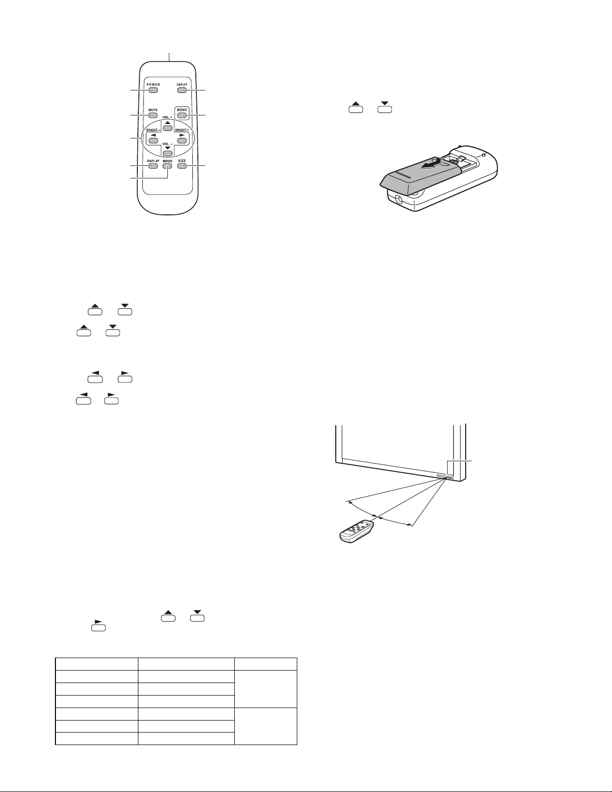
■ Remote Control Unit
2
3
4
1
7
8
*1 Select the terminal for DVI SELECT.
*2 Select the terminal for BNC SELECT.
8MENU button
Displays and turns off the menu screen
9SIZE button
The menu is displayed.
Press or to select the screen size.
■ Setting the batteries
1) Press the cover gently and slide it in the direction of the arrow.
5
9
6
1Signal transmitter
2POWER button
3MUTE button
Turns off the volume temporarily.
Press the MUTE button again to turn the sound back to the previous
level.
4VOL +/- button (Volume adjustment)
Pressing or displays the VOLUME menu when the menu
screen is not displayed.
Press or to adjust the volume of the sound.
*If you do not press any buttons for about 4 seconds, the VOLUME
menu automatically disappears.
BRIGHT
+/− button (Backlight adjustment)
Pressing or displays the BRIGHT menu when the menu
screen is not displayed.
Press or to adjust the brightness.
*If you do not press any buttons for about 4 seconds, the BRIGHT
menu automatically disappears.
Cursor control (S /T/W / X) buttons
5DISPLAY button
Displays monitor information. The display disappears when this button is
pressed again or disappears automatically after approximately
15 seconds.
6MODE button
Each time you press this button, the color mode changes in the following order:
• STD (Standard) JVIVID J sRGB
J STD...
*sRGB applies to PC input only.
sRGB is international standard of color representation specified by
IEC (International Electrotechnical Commission).
Color conversion is made in taking account of liquid crytal’s characteristics and represents color tone close to its original image.
7INPUT button (Input mode selection)
The menu is displayed. Press or to select the input mode,
and press to enter.
*You can select the input terminal by pressing the input switch of
the monitor.
Input mode Video Audio
PC1 DIGITAL
PC2 ANALOG PC2 input terminal
PC3 ANALOG
AV1 DIGITAL
AV2 COMPONENT
*1
PC1 input terminal PC audio input
terminal
*2
*1
PC3 input terminals
AV1 input terminal AV audio input
*2
AV2 input terminals
terminals
AV3 VIDEO AV3 input terminal
2) See the instructions in the compartment and put in the supplied batteries (2 “AA” size batteries) with their plus (
+) and minus (−) sides
oriented correctly.
3) Close the cover.
Note:
• The supplied batteries (2 “AA” size batteries) may become
exhausted faster depending on the storage condition. It is recommended that you replace them with new batteries (commercially
available) earlier than specified.
• If you will not use the remote control for a long time, remove the
batteries.
• Use manganese or alkaline batteries only.
■ Remote control operation range
The operation range of the remote control unit is approx. 16.4 feet (5m)
at an angle of appro
the remote control sensor.
16.4 feet (5 m)
°
10
Caution:
• Do not expose the remote control unit to shock by dropping or stepping on it. This could lead to a malfunction.
• Do not expose the remote control unit to liquids, and do not place it
in an area with high humidity.
• The remote control unit may not work properly if the remote control
sensor is under direct sunlight or strong lighting.
• Objects between the remote control unit and the remote control
sensor may prevent proper operation.
• Replace the batteries when they run low as this may shorten the
remote control’s operation range.
• If a fluorescent light is illuminated near the remote control unit, it
may interfere with proper operation.
• Do not use it with the remote control of other equipment such as air
conditioner, stereo components, etc.
× 10° from the center to the top/bottom/right/left of
Remote control sensor
16.4 feet
(5 m)
16.4 feet (5 m)
°
10
PN-525U OUTLINE OF THE PRODUCT, NOMENCLATURE AND FUNCTION
1 – 4
Page 7
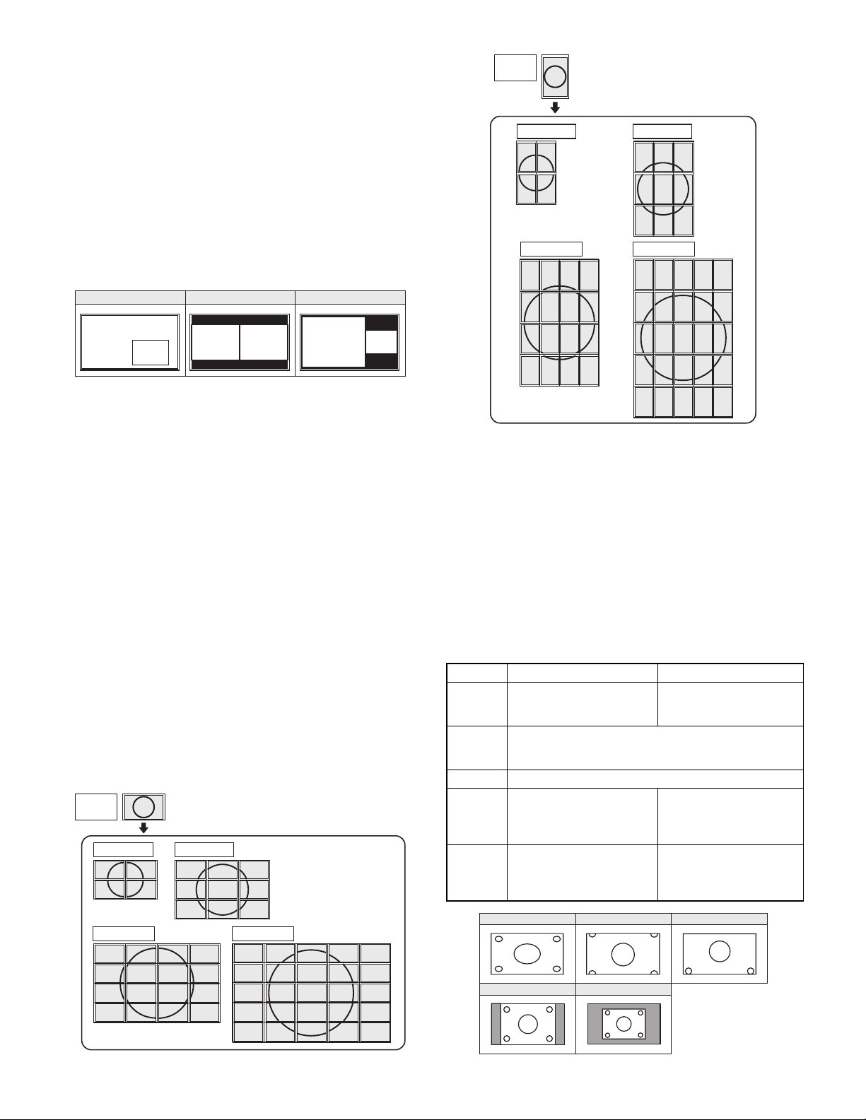
■ Dual screen display
1
3
0
2
012
456
8
9
10
3
7
11
12 13 14 15
012
567
10
11 12
3
8
13
15 16 17 18
20 21 22 23
4
9
14
19
24
012
345
678
1
3
02
0
1
2
4
5
6
8
9
10
3
7
11
12
13
14
15
0
1
2
5
6
7
10
11
12
3813
15
16
17
18
20
21
22
23
4
9
141924
0
1
2
3
4
5
6
7
8
You can display the screens of the PC input signal and AV input signal
simultaneously.
Set this function with “PIP MODES” in the PIP/PbyP menu.
• The currently selected input signal is displayed on the main screen.
• You cannot simultaneously display the screens of signals of the same
type, such as two types of PC input signals or two types of AV input
signals.
PIP : A sub screen is displayed inside a main screen.
PbyP : A main screen and a sub screen are displayed in a line.
PbyP2 : Displays a main screen which measures 1280 pixels in the
longest direction and a sub screen in a line.
In vertical orientation
Original
image
4 monitors
02
1
3
16 monitors 25 monitors
8
12
9 monitors
0
3
6
1
4
7
2
5
8
0
5
10
15
0
4
20
PI P PbyP PbyP2
Main screen
screen
Sub
Main
screen
Sub
screen
Main screen
Note:
• You might infringe on a copyright of the author which is protected
by copyright law when you display the images of the computer
screen and television/VCR simultaneously for profit-making or to
show the image to the public.
• The screen size for dual-screen display is the same as the screen
size for single-screen display. The DotbyDot screen is displayed in
NORMAL size except when it is set as the PIP main screen.
• When dual-screen display is selected, the SCREEN MOTION func-
tion is disabled.
• When dual-screen display is selected, the AUTO INPUT CHANGE
function is disabled.
• When dual-screen display is selected, the screen cannot be
enlarged.
• When dual-screen display is selected, the following adjustments of
ADVANCED are invalid and adjusting is disabled.
3D-NR, MPEG-NR and 3D-Y/C
■ Enlarge
You can align 4, 9, 16, or 25 monitors and integrate them into a single
large screen to display.
Enlarged views of separated images are displayed in each monitor.
In horizontal orientation
Original
image
4 monitors
0
2
16 monitors 25 monitors
012
456
8
12 13 14 15
9 monitors
1
3
910
012
345
678
11
3
7
012
567
10
15 16 17 18
20 21 22 23
11 12
13
PN-525U OUTLINE OF THE PRODUCT, NOMENCLATURE AND FUNCTION
21
2
7
12
17
22
18
23
3813
4
9141924
Sub
screen
1
5
9
13
2
6
10
14
3
711
15
1
6
11
16
Note:
• AV input signals cannot be used for the Enlarge function.
• To integrate 9 or more monitors using PC1 signals, a splitter for the
video signal (commercially available) is required.
• When Enlarge is used, the AUTO INPUT CHANGE function is disabled.
• When connected in PC2/PC3, a splitter for the video signal (commercially available) is required.
• When Enlarge is used, the SCREEN MOTION function is disabled.
■ Switching the screen size
Even when the screen size is changed, the display may remain the
same depending on the input signal.
PC input AV input
WIDE Displays image so it fills the
entire screen.
ZOOM 1 An image with a 4:3 aspect ratio is enlarged to fill the
entire screen without changing the aspect ratio. The
edges of the image may be cut off.
ZOOM 2 Use this size if ZOOM 1 cuts off the subtitles.
NORMAL Displays image so it fills the
screen without changing the
aspect ratio of the input sig-
nals.
DotbyDot Displays the dots of the sig-
nals input from the conne-
cted PC as the correspond-
ing dots on the screen.
WIDE ZOOM1
3
4
8
9
14
19
24
NORMAL
DotbyDot
1 – 5
An image with a 4:3 aspect
ratio is stretched to fill the
entire screen.
Displays the entire image
of the aspect ratio of 4:3
without changing the
aspect ratio.
Displays the dots of the
input signals as the corresponding dots on the
*
screen.
ZOOM2
Page 8
*With a monitor with a screen resolution of 1600 x 1200, selecting Dot-
byDot displays the NORMAL screen.
Note:
• Using this monitor's screen-size switching or dual-screen display
functions to compress or expand the screen for commercial or public viewing in establishments like cafes or hotels may infringe on
the rights of the creators, as protected by Copyright Law, so please
be careful.
• When “Enlarge” is set, the screen size is fixed to “WIDE” mode.
• When dual-screen display is selected, the screen size cannot be
changed.
• The appearance of the original video may change if you select a
screen size with a different aspect ratio than the original image
(e.g. TV broadcast or video input from external equipment).
• When an ordinary non-wide image (4:3) is viewed with the whole
screen using the screen-size switching function of this monitor, the
edge of the image may be lost or appear distorted. If you wish to
respect the creator’s intentions, set the screen size to “NORMAL”.
• When playing commercial software, parts of the image (like subtitles) may be cropped. In this case select the optimal screen size
using the screen-size switching function of this monitor. With some
software, there may be noise or distortion at the edges of the
screen. This is due to the characteristics of the software, and is not
a malfunction.
• Depending on the original image size, black bands may remain at
the edges of the screen.
■ SCHEDULE
You can set the time to switch the monitor on and off.
Set this function with “SCHEDULE” in the OPTION menu.
SCHEDULE
No. POWER DAY OF THE WEEK TIME INPUT
(1)
XXXX/XX/XX XXX XX:XX:XX
(2)
PC2 ANALOG
(3) (4) (5)
Specifies the day of the week to execute the SCHEDULE.
ONLY ONCE:
Executes the SCHEDULE once on the specified day.
Specify the day of the week to execute the SCHEDULE.
EVERY WEEK:
Executes the SCHEDULE on the specified day of the week every
week. Specify the day of the week to execute the SCHEDULE.
Periodic setting such as “Monday through Friday” is also possible.
EVE RY DAY:
Executes the SCHEDULE every day regardless of the day of the
week.
4 TIME
Specifies the time to execute the SCHEDULE.
Set the time on a 24-hour basis.
5 INPUT
Specifies the input mode at power-on. When not specifying, the
screen at the previous power-off appears.
Input modes displayed on “PC1/AV1” depend on DVI SELECT settings.
Input modes displayed on “PC3/AV2” depend on BNC SELECT settings.
Caution:
• Do not switch off the main power after setting the SCHEDULE.
• Specify the correct date and time.
SCHEDULE does not function unless the date and time are specified.
• Check regularly that the set date and time are correct.
Note:
• Up to 8 SCHEDULE items can be registered.
• Setting the SCHEDULE flashes the power LED alternately in red and
orange in standby mode.
• A SCHEDULE that has a large number has precedence over that of a
small number when schedules overlap.
1024x768
V: 60 Hz H: 48.4 kHz
OK…[MENU]
1) Press or to select the SCHEDULE number, and press
.
2) Set the SCHEDULE. (See the description below.)
Press or to select the date and time, and press or
to change the setting.
3) Press .
MENU
SCHEDULE becomes effective.
1
Q : SCHEDULE effective
-
: SCHEDULE not effective
2 POWER
ON : Switches the monitor on at the specified time.
OFF : Switches the monitor off at the specified time and puts the
monitor in standby mode.
3 DAY OF THE WEEK
■ ADVANCED items (AV input)
FLESH TONE
Adjust the hue control.
3D-NR
Reduce the noise of playback images on video.
Setting a higher level reduces more noise. However, it may cause blurring on an image.
MPEG-NR
Reduce block noise caused by digital compression.
3D-Y/C (AV3)
Specify whether to perform 3-dimension Y/C separation.
If dot interference or cross-color is occurring in fast-motion scenes,
selecting “OFF” may improve the image quality.
PN-525U OUTLINE OF THE PRODUCT, NOMENCLATURE AND FUNCTION
1 – 6
Page 9
CHAPTER 2. CONNECTION, ADJUSTMENT, OPERATION, AND FUNCTION
1. CONNECTION
1-1. CONNECTING PERIPHERAL EQUIPMENT
Caution:
• Be sure to turn off the main power switch and disconnect the plug
from the power outlet before connecting/disconnecting cables.
Also, read the manual of the equipment to be connected.
• Be careful not to mix up the input terminal with the output terminal
when connecting cables. Mixing up the input and output terminals
may cause malfunctions and the other problems.
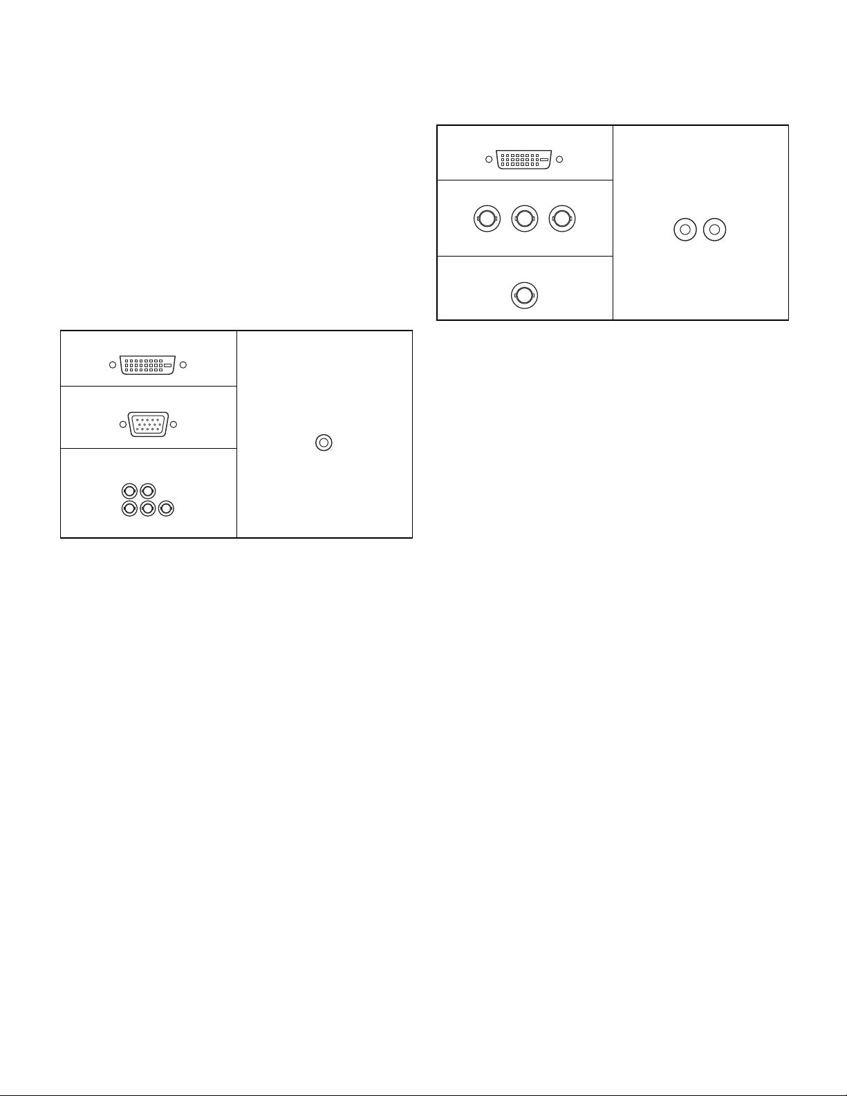
(1) Connection with a PC
PC1 input terminal
PC2 input terminal
PC audio input terminal
PC3 input terminals
HV
RGB
• Use a commercially available signal cable (DVI-D 24 pin) for the PC1
input terminal. Set DVI SELECT on the OPTION menu to PC (DIGITAL) when using the PC1 input terminal.
• Use a commercially available signal cable (Mini D-sub 15 pin) for the
PC2 input terminal.
• Use a commercially available signal cable (BNC) for the PC3 input
terminals. Set BNC SELECT on the OPTION menu to PC (ANALOG)
when using the PC3 input terminals.
(2) Connection with AV equipment
AV1 input terminal
AV2 input terminals
Cr/Pr Y Cb/Pb
AV3 input terminal
• Use a commercially available signal cable (DVI-D 24 pin) for the AV1
input terminal. Set DVI SELECT on the OPTION menu to AV (DIGITAL) when using the AV1 input terminal.
• Use a commercially available component cable (BNC) for the AV2
input terminals. Set BNC SELECT on the OPTION menu to AV
(COMPONENT) when using the AV2 input terminals.
• Use a commercially available video cable (BNC) for the AV3 input terminal.
• Use a commercially available audio cable (RCA) for the AV audio
input terminals.
• The AV1 input terminal is compatible with the video signals below:
1920
× 1080p @ 50/59.94/60Hz
1920
× 1080i @ 50/59.94/60Hz
1280
× 720p @ 50/59.94/60Hz
720
× 576p @ 50Hz
720
× 480p @ 59.94/60Hz
640
× 480p @ 59.94/60Hz
• The AV2 input terminals are compatible with the video signals below :
1080i (1125i)/50, 1080i (1125i)/60, 720p (750p)/50, 720p (750p)/60,
576p (625p), 576i (625i), 480p (525p), 480i (525i)
AV audio input terminals
• Use a commercially available audio cable (mini stereo jack) for the
PC audio input terminal. Use an audio cable without resistance.
Note:
• Images may not be displayed properly depending on the computer
(graphics board) to be connected.
• A screen with 1920
rectly on PC3 (BNC). In this case, check the settings of your computer (graphics board) to verify that input signals conform to
specifications of this monitor (Hsync: 66.3 kHz, Vsync: 60 Hz, and
Dot frequency: 148.5 MHz).
• If there is a check box to disable EDID in display control panel,
check it when using PC3 (BNC).
• Use the automatic screen adjustment when a PC screen is dis-
played for the first time using PC2 or PC3, or when the setting of
the PC is changed.
• The screen is adjusted automatically when SELF ADJUST in the
OPTION menu is set to “ON”.
× 1080 resolution may not be displayed cor-
PN-525U CONNECTION, ADJUSTMENT, OPERATION, AND FUNCTION
2 – 1
Page 10
(3) Other terminals
[PC/AV audio output terminals]
• Audio from the equipment connected to the AV audio input terminals
or PC audio input terminal is output. Connect to the audio input terminals of the connected equipment using a commercially available
audio cable (RCA).
• The audio output varies depending on the input mode selection.
• The volume level can be adjusted using the volume adjustment.
• Selecting FIXED of “AUDIO OUTPUT” from the OPTION menu fixes
the volume of sound output from the audio output terminals.
Caution:
• Do not use a power cord other than the one supplied with the monitor.
• Be sure to use a power outlet of AC 120 V (60 Hz).
Using power supply other than the one specified may cause fire.
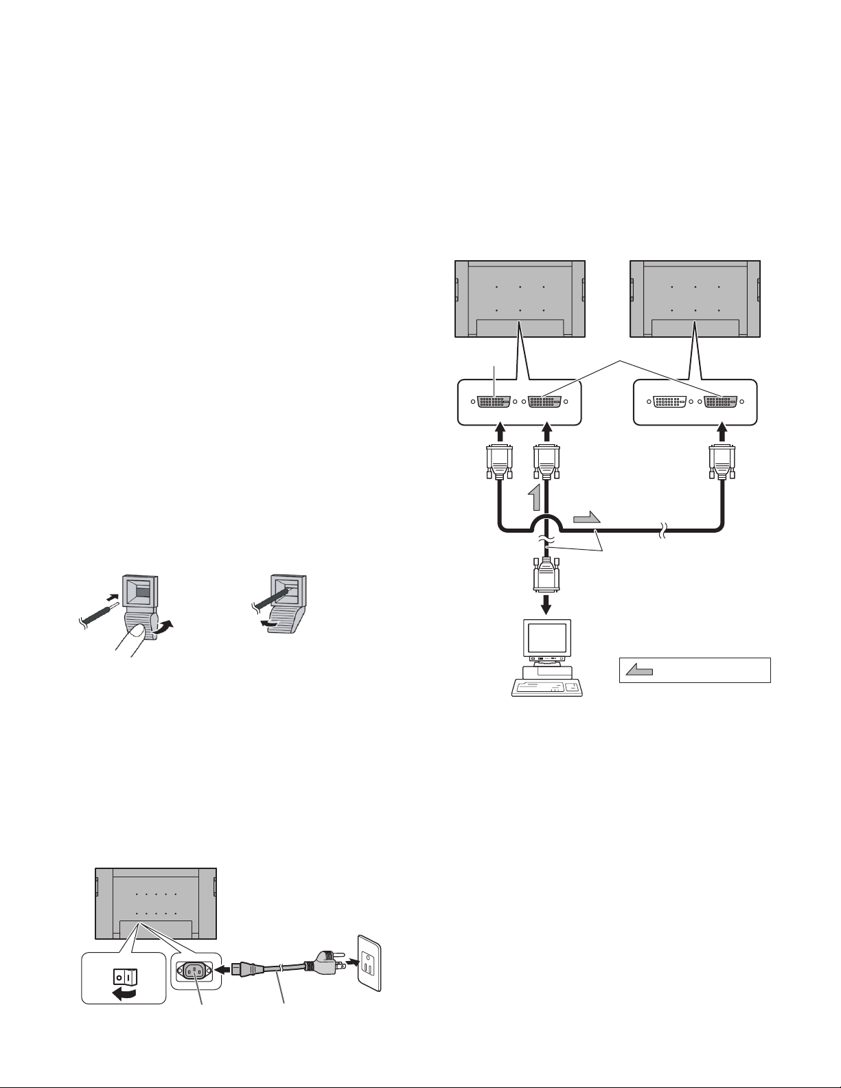
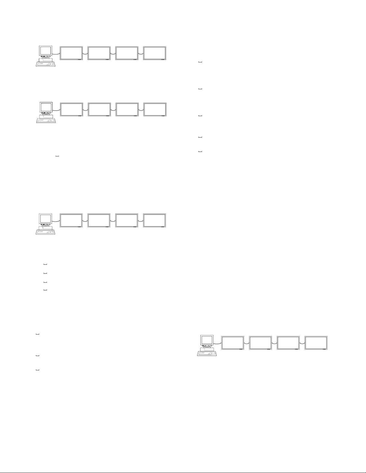
1-4. CONNECTING MULTIPLE MONITORS
You can connect multiple monitors (up to 5 monitors) in a daisy chain by
using the PC1/AV1 input terminals and PC/AV output terminals of this
monitor.
[Connection example]
• Audio signals output from the PC/AV audio output terminals cannot
be adjusted using the AUDIO menu.
[PC/AV output terminals]
Video signals from PC1 and AV1 can be output to HDCP-compatible
external device. Use this terminal when you connect multiple monitors in a daisy chain via DVI cable (commercially available).
Images cannot be output to device that is not HDCP-compatible.
[RS-232C input/output terminals]
You can control the monitor from a PC by connecting a commercially
available RS-232C straight cable between this terminal and the PC.
1-2. CONNECTING EXTERNAL SPEAKERS
Be sure to use external speakers with an impedance of 6 ohms and a
rated input of at least 7W.
1) While pushing the tab, insert the tip of the cable.
2) Release the tab.
12
First monitor Second monitor
PC/AV output
PC1/AV1 input terminals
terminal
Digital signal (DVI) cables
(commercially available)
To PC digital RGB output terminal
Note:
• Be sure to connect the
speakers properly.
• Avoid short circuiting the
+ and − terminals and the left and right
+ and − terminals.
1-3. CONNECTING THE POWER CORD
1) Turn off the main power switch.
2) Plug the power cord (supplied) into the AC input terminal.
3) Plug the power cord (supplied) into the AC power outlet.
Power outlet
Main power switch
1
AC input terminal
2
Power cord (Supplied)
3
PN-525U CONNECTION, ADJUSTMENT, OPERATION, AND FUNCTION
shows the signal flow
Note:
• The length of the signal cables or surrounding environment may
affect the image quality.
• The screen may not display properly when using terminals other
than PC1/AV1 for the input mode. In this case, turn off the power to
all the monitors connected in a daisy chain and then turn the power
on again.
2 – 2
Page 11
1-5. CONTROLLING THE MONITOR WITH A PC
You can control this monitor from a PC via RS-232C (COM port) on the
PC. You can also connect multiple monitors via a daisy chain by using a
PC. By assigning ID numbers to each monitor, you can make input
mode selection/adjustment or can check the status of
■ PC connection
One-to-one connection with a PC
Connect with RS-232C straight cable between the PC’s COM port
(RS-232C connector) and the RS-232C input terminal on the rear of the
monitor.
RS-232C input terminal
To COM port
RS-232C straight cable
(commercially available)
Daisy chain connection from a single PC (Advanced operation)
Connect with RS-232C straight cable between the PC’s COM port
(RS-232C connector) and the RS-232C input terminal on the rear of the
first monitor.
Next, connect RS-232C straight cable to the first monitor’s RS-232C
output terminal and to the second monitor’s RS-232C input terminal.
Connect in the same way to the third and subsequent monitors.
First monitor Second monitor
a specific
monitor.
PC
1-6. HOW TO INSTALL THE MONITOR
■ Mounting precautions
• Since the monitor is heavy, consult your dealer before installation.
• Installing or moving the monitor must be done by two or more people.
• A stand and mounting bracket compliant with VESA specifications is
required. Do not use any screw holes other than VESA holes for
installation.
• When moving the monitor, be sure to hold it with the handles both on
the rear and the unit bottom. Do not hold the LCD panel. This may
cause product damage, failure, or injury.
• Install the monitor with the surface perpendicular to a level surface. If
necessary, limit the tilt between 0 and 20 degrees downward.
• Mounting the monitor on the wall requires special expertise and the
work must be performed by an authorized SHARP dealer. You should
never attempt to perform any of this work yourself. Our company will
bear no responsibility for accidents or injuries caused by improper
mounting or mishandling.
• This monitor should be used at an ambient temperature between
32 °F (0 °C) and 104 °F (40 °C). Provide enough space around the
monitor to prevent heat from accumulating inside.
For the monitor in
horizontal orientation
7-7/8 [20]
2
[5]
2 [5]
**
2
[5]
For the monitor in
vertical orientation
7-7/8
[20]
2
[5]
2
[5]
RS-232C
output
terminal
RS-232C
input
PC
To COM port
terminal
RS-232C straight cables
(commercially available)
■ Communication conditions
Set the RS-232C communication settings on the PC to match the
monitor’s communication settings as follows:
Baud rate 9,600bps
Data length 8bits
Parity bit None
Stop bit 1bit
Flow control None
Unit: inch [cm]
*The monitor can be installed close to a wall, etc.
However, the monitor emits heat during operation. Be aware that
heat emitted from the monitor may discolour or alter the wall.
If it is difficult to provide such space because the monitor is
installed inside a housing or for other reasons, take other measures
to keep the ambient temperature between 32°F (0 °C) and 104 °F
(40 °C) such as installing a fan in the housing.
• Adhere to the following when installing the monitor in the vertical
orientation. Failing to adhere to the following may cause malfunctions.
-
Install the monitor such that the power LED is located on the
downside.
-
Set the MONITOR on the SETUP menu to PORTRAIT.
• Do not block any ventilation openings. If the temperature inside the
monitor rises, this could lead to a malfunction.
• After mounting, it is recommended to take some measures to pre-
vent the monitor from falling down.
• Do not place the monitor on a device which generates heat.
• Be sure to use a stand or a wall-mount/ceiling-mount bracket
designed or designated for mounting the monitor.
2 [5]
PN-525U CONNECTION, ADJUSTMENT, OPERATION, AND FUNCTION
2 – 3
Page 12
• This monitor is designed to be installed on a concrete wall/ceiling or
pillar. Reinforced work might be necessary for some materials such
as plaster/thin plastic board/wood before starting installation.
This monitor and bracket must be installed on a wall which can
endure at least 4 times or more the weight of the monitor. Install by
the most suitable method for the material and the structure.
• Use the supplied logo sticker when you install the monitor in vertical orientation.
*
INPUT
*Do not remove the factory-affixed sticker but affix the logo sticker
over it.
Be careful not to cover the remote control sensor or buttons.
■ BINDING CABLES
[Attaching the cable clamp]
The cables connected to the terminals on the back of the monitor can
be neatly bundled using the supplied cable clamps as shown in the illustration.
Caution:
• Verify the position for attaching a cable clamp in advance.
• A cable clamp cannot be removed once it is attached.
[Fastening the power cord]
1) Attach the supplied power cord clamp to the power cord, making
sure the power cord clamp is circular hole-sidedown.
2) Insert the tip of the band into the hole for the power cord clamp.
3) While holding the tail of the band, slide the fastened part toward the
AC input terminal.
Cable clamp
positions
Insert the cable
Cable clamp
attachment
clamp into a hole.
(any hole available)
Cable clamp
123
Hole for
the power
cord clamp
Fastened
part
Band
Power cord
clamp
PN-525U CONNECTION, ADJUSTMENT, OPERATION, AND FUNCTION
2 – 4
Page 13
2. ADJUSTMENT METHOD
[ADJUSTMENTS FOR PC SCREEN DISPLAY]
■ Automatic adjustment
When you use the PC2 input terminal or PC3 input terminals to display
a PC screen for the first time, or when you change the setting of the PC,
use the automatic screen adjustment.
1) Switch the input to PC2 or to PC3 and display the adjustment pattern. (See the description below.)
2) Press and use or to display the SCREEN menu.
MENU
3) Press and select “AUTO”.
4) Press .
The automatic adjustment is complete in several seconds.
5) Press twice to close the menu screen.
MENU
Note: If the screen cannot be adjusted properly with one automatic
adjustment, repeat the automatic adjustment two or three times.
Try manual adjustment if necessary.
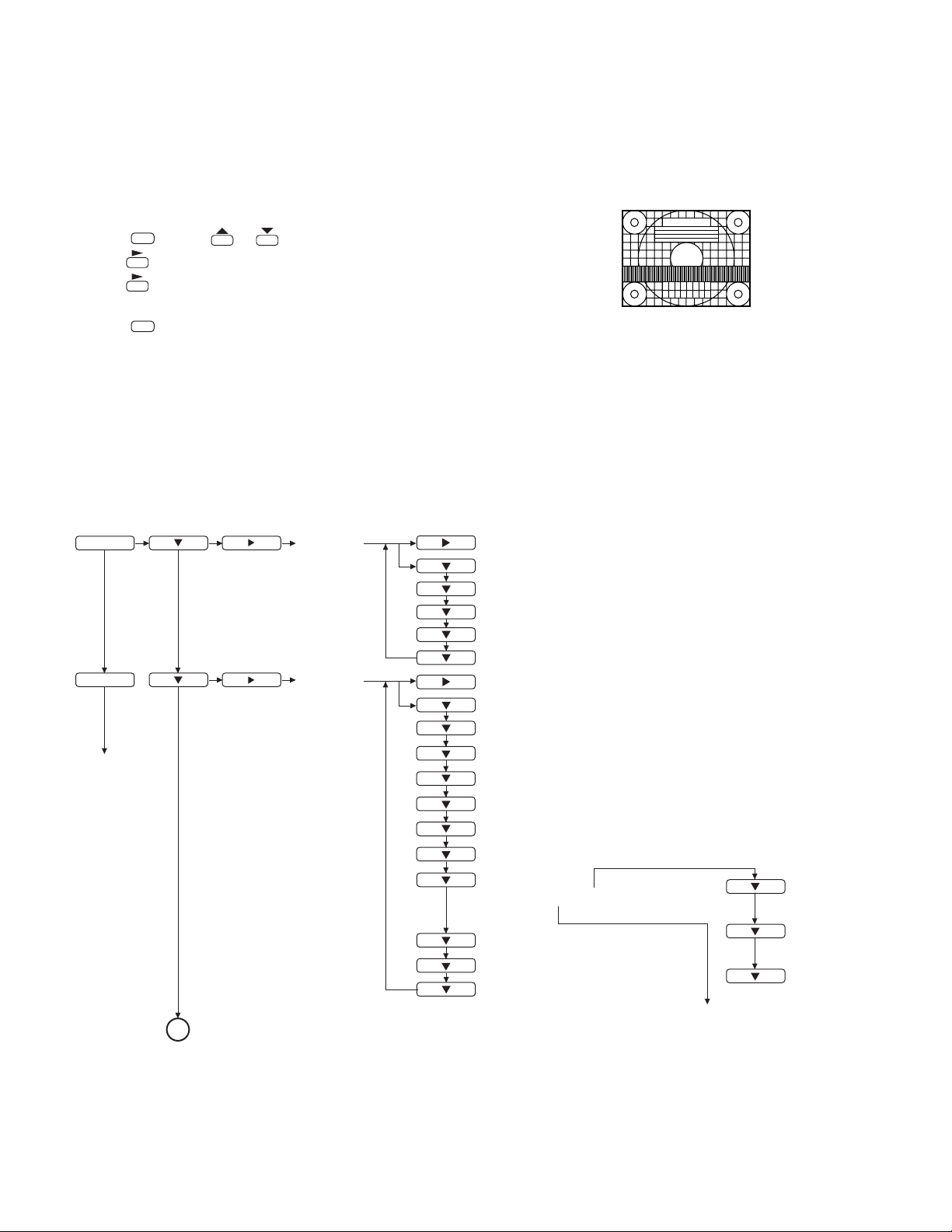
■ Screen display for adjustment
Before making adjustments in the SCREEN menu or PICTURE menu,
display an image to brighten the entire screen. If you are using a Windows PC, use the adjustment pattern on the supplied CD-ROM.
2-1. SETTINGS AND ADJUSTMENTS
<Opening the adjustment pattern>
1) Load the supplied CD-ROM into the computer's CD-ROM drive.
2) Open the CD-ROM in [My Computer].
3) Double-click [Adj_uty.exe].
The adjustment pattern will appear.
Adjust the screen automatically or manually.
4) When adjustment is finished, press the [Esc] on the computer's keyboard to quit the adjustment program.
5) Eject the CD-ROM from the CD-ROM drive.
Note: If the display mode on the computer you are using is 65,000 col-
ors, the color levels in the color pattern may appear differently or
grayscale may appear to be colored.
(This is due to the specifications of the input signal and is not a
malfunction.)
MENU
MENU
END
SCREEN
(PC2/PC3)
PICTURE
AUTO
CLOCK
PHASE
H-POS
V-POS
RESET
(Adjust with
(Adjust with
(Adjust with
(Adjust with
(Initialize with
AUTO (PC2/PC3)
CONTRAST
BLACK LEVEL
TINT (AV input)
COLORS (AV input)
SHARPNESS
ADVANCED (AV input)
COLOR MODE
WHITE BALANCE
*
(THRU /PRESET/USER)
COPY TO USER
GAMMA
RESET
(Adjust with
(Adjust with
(Adjust with
(Adjust with
(Adjust with
(Adjust with
(Adjust with
(Adjust with
(Adjust with
(Adjust with
(Initialize with
e and d.)
e and d.)
e and d.)
e and d.)
d.)
e and d.)
e and d.)
e and d.)
e and d.)
e and d.)
e and d.)
e and d.)
e and d.)
d.)
e and d.)
d.)
R-CONTRAST
(Adjust with e and d.)
G-CONTRAST
(Adjust with
e and d.)
B-CONTRAST
(Adjust with
e and d.)
A
PN-525U CONNECTION, ADJUSTMENT, OPERATION, AND FUNCTION
* Input signal level (for PC1 only)
PRESET
(Adjust with
e and d.)
2 – 5
Page 14
A
AUDIO
SETUP
OPTION
TREBLE
BASS
BALANCE
RESET
OSD H-POSITION
OSD V-POSITION
SCREEN MOTION
MOTION TIME 1
MOTION TIME 2
MONITOR
LANGUAGE
ID No. SET
PICTURE FLIP
POWER ON DELAY
DATE/TIME SETTING
SCHEDULE
DVI SELECT
BNC SELECT
QUICK SHOOT
COLOR SYSTEM
AUDIO OUTPUT
480LINES (PC2/PC3)
(Adjust with e and d.)
(Adjust with
(Adjust with
e and d.)
e and d.)
(Initialize with d.)
(Adjust with
(Adjust with
e and d.)
e and d.)
(Adjust with e and d.)
(Adjust with
(Adjust with
(Adjust with
(Adjust with
(Adjust with
(Adjust with
(Adjust with
(Adjust with
(Adjust with
(Adjust with
(Adjust with
e and d.)
e and d.)
e and d.)
e and d.)
e and d.)
e and d.)
e and d.)
e and d.)
e and d.)
e and d.)
e and d.)
(Adjust with e and d.)
(Adjust with
(Adjust with
(Adjust with
e and d.)
e and d.)
e and d.)
ENLARGE
(PC input)
PIP/PbyP
768LINES (PC2/PC3)
SELF ADJUST
POWER MANAGEMENT
AUTO INPUT CHANGE
ENLARGE MODE
ENLARGE POS
BEZEL H
BEZEL V
H-POS
V-POS
PIP MODES
PIP SIZE
PIP H-POS
PIP V-POS
PIP BLEND
PIP SOURCE
SOUND CHANGE
MAIN POS
PbyP2 POS
(Adjust with
(Adjust with
(Adjust with
e and d.)
e and d.)
e and d.)
(Adjust with e and d.)
(Adjust with
(Adjust with
(Adjust with
e and d.)
e and d.)
e and d.)
(Adjust with e and d.)
(Adjust with
(Adjust with
(Adjust with
(Adjust with
(Adjust with
(Adjust with
(Adjust with
(Adjust with
(Adjust with
(Adjust with
(Adjust with
e and d.)
e and d.)
e and d.)
e and d.)
e and d.)
e and d.)
e and d.)
e and d.)
e and d.)
e and d.)
e and d.)
AUTO OFF
(Adjust with
* The menu screen will close automatically if no operation is performed for about 15 seconds.
PN-525U CONNECTION, ADJUSTMENT, OPERATION, AND FUNCTION
2 – 6
e and d.)
Page 15
2-2. INITIALIZATION (RESET)/FUNCTIONAL RESTRICTION SETTING
SIZE
(Press about 5 seconds.)
MENU
ALL RESET
ADJUSTMENT LOCK
OSD DISPLAY
LED
RS-232C
(Adjust with
(Adjust with
(Adjust with
(Adjust with
(Adjust with
END
2-3. ADJUSTMENT ITEM LIST
INPUT MODE ITEM ADJUSTMENT
PC1 PC2 PC3 AV1 AV2 AV3 SCREEN AUTO
¥¥ CLOCK 0 ~ 255
¥¥ PHASE 0 ~ 63
¥¥ H-POS 0 ~ 100
¥¥
¥¥
¥¥ PICTURE AUTO
¥¥¥¥¥¥
¥¥¥¥¥¥
¥¥¥ TINT 0 ~ 60
¥¥¥ COLORS 0 ~ 60
¥¥¥¥¥¥ SHARPNESS 0 ~ 24
¥¥¥
¥¥¥
¥¥¥
¥
¥¥¥¥¥¥
¥¥¥¥¥¥
¥¥¥¥¥¥
¥¥¥¥¥¥ R-CONTRAST 0 ~ 512
¥¥¥¥¥¥ G-CONTRAST 0 ~ 512
¥¥¥¥¥¥ B-CONTRAST 0 ~ 512
¥¥¥¥¥¥
¥¥¥¥¥¥ GAMMA 1.8/2.2/2.4
¥¥¥¥¥¥
V-POS Depends on the resolution
Either 0 ~ 200/300/500
RESET OFF
ON
CONTRAST PC1/AV1/AV2/AV3: 0 ~ 60
PC2/PC3: 0 ~ 127
BLACK LEVEL PC1/AV1/AV2/AV3: 0 ~ 60
PC2/PC3: 0 ~ 127
ADVANCED FLESH TONE OFF
LOW
HIGH
3D-NR OFF
LOW
HIGH
MPEG-NR OFF
ON
3D-Y/C OFF
ON
COLOR MODE STD
VIVID
sRGB
WHITE BALANCE THRU (PC1 only)
PRESET
USER
PRESET 3000K ~ 10000K
(500K carve)
COPY TO USER OFF
ON
RESET OFF
ON
e and d.)
e and d.)
e and d.)
e and d.)
e and d.)
*2
PN-525U CONNECTION, ADJUSTMENT, OPERATION, AND FUNCTION
2 – 7
Page 16
INPUT MODE ITEM ADJUSTMENT
¥¥¥¥¥¥AUDIO TREBLE
¥¥¥¥¥¥ BASS
¥¥¥¥¥¥ BALANCE
¥¥¥¥¥¥
¥¥¥¥¥¥SETUP OSD H-POSITION 0 ~ 100
¥¥¥¥¥¥ OSD V-POSITION 0 ~ 100
¥¥¥¥¥¥
¥¥¥¥¥¥ MOTION TIME 1 0 ~ 20 (H) [Unit: hour]
¥¥¥¥¥¥
¥¥¥¥¥¥
¥¥¥¥¥¥
¥¥¥¥¥¥ ID No. SET 0 ~ 255
¥¥¥¥¥¥
¥¥¥¥¥¥ POWER ON DELAY 0 ~ 60 (S) [Unit: second]
¥¥¥¥¥¥OPTION DATE/TIME SETTING Year: 2007 ~ 2099
¥¥¥¥¥¥ Month: 1 ~ 12
¥¥¥¥¥¥ Day: 1 ~ 28, 29, 30, 31
¥¥¥¥¥¥ Time: 00:00 ~ 23:59
¥¥¥¥¥¥
¥¥¥¥¥¥
¥¥¥¥¥¥
¥¥¥¥¥¥
¥¥¥¥¥¥
¥¥¥¥¥¥ TIME 00:00 ~ 23:59
¥¥¥¥¥¥
¥¥¥¥¥¥
RESET OFF
SCREEN MOTION OFF
MOTION TIME 2 PATTERN1: 10 ~ 990 (S)
MONITOR LANDSCAPE
LANGUAGE ENGLISH/DEUTSCH/FRANCAIS/
PICTURE FLIP STANDARD
SCHEDULE (Set
DVI SELECT PC (DIGITAL)
--- or ¥ )
POWER OFF
DAY OF THE WEEK ONLY ONCE
INPUT ---
−10 ~ 0 ~ +10
−10 ~ 0 ~ +10
−10 ~ 0 ~ +10
ON
PATTERN1
PATTERN2
PATTERN3
PATTERN4
PATTERN2/3/4: 5 ~ 20 (S) [Unit: second]
PORTRAIT
ITALIANO/ESPANOL/PYCCKNÑ/
Japanese
MIRROR
UPSIDE DOWN
ROTATE
--- (Invalidity)
¥ (Effectriely)
ON
EVERY DAY
EVERY WEEK
MON
TUE
WED
THU
FRI
SAT
SUN
--MON
TUE
WED
THU
FRI
SAT
SUN
PC1/AV1
PC2
PC3/AV2
AV3
AV (DIGITAL)
PN-525U CONNECTION, ADJUSTMENT, OPERATION, AND FUNCTION
2 – 8
Page 17

INPUT MODE ITEM ADJUSTMENT
¥¥¥¥¥¥
¥¥¥¥¥¥
¥¥¥¥¥¥
¥¥¥¥¥¥
¥¥
¥¥
¥¥¥¥¥¥
¥¥¥¥¥¥
¥¥¥¥¥¥
¥¥¥
¥¥¥
¥¥¥ BEZEL H 0 ~ 100
¥¥¥ BEZEL V 0 ~ 100
¥¥¥ H-POS infinite
¥¥¥ V-P OS in finite
¥¥¥¥¥¥
¥¥¥¥¥¥ PIP SIZE 1 ~ 12
¥¥¥¥¥¥ PIP H-POS 0 ~ 100
¥¥¥¥¥¥ PIP V-POS 0 ~ 100
¥¥¥¥¥¥ PIP BLEND 0 ~ 15
¥¥¥¥¥¥ PIP SOURCE
¥¥¥¥¥¥
¥¥¥¥¥¥
¥¥¥¥¥¥
¥¥¥¥¥¥
OPTION BNC SELECT PC (ANALOG)
QUICK SHOOT OFF
COLOR SYSTEM AUTO
AUDIO OUTPUT VARIABLE
480 LINES 640
768 LINES 1024
SELF ADJUST OFF
POWER MANAGEMENT OFF
AUTO INPUT CHANGE OFF
ENLARGE ENLARGE MODE OFF
ENLARGE POS 2
PIP/PbyP PIP MODES OFF
SOUND CHANGE MAIN
MAIN POS POS1
PbyP2 POS POS1
AUTO OFF MANUAL
AV (COMPONENT)
ON
PA L
PAL-60
SECAM
NTSC3.58
NTSC4.43
FIXED
× 480
× 480
848
1280
1360
ON
ON
ON
× 2
2
× 3
3
× 4
4
× 5
5
× 2: 0 ~ 3
× 3: 0 ~ 8
3
× 4: 0 ~ 15
4
× 5: 0 ~ 24
5
PIP
PbyP
PbyP2
SUB
POS2
POS2
POS3
AUTO
× 768
× 768
× 768
PN-525U CONNECTION, ADJUSTMENT, OPERATION, AND FUNCTION
2 – 9
Page 18

2-4. 232C CONTROL
(1) Communication procedure
<Command format>
When a command is sent from the PC to the monitor, the monitor operates according to the received command, and sends a response message to the PC.
■ When a command has not been executed
Return code (0DH, 0AH)
RRE
*If an ID number has been assigned
Return code
C1 C2 C3 C4 P1 P2 P3 P4
Command field
(4 prescribed
alphanumerical
characters)
Parameter field
(4 character string
comprised of:
0-9, +, -, space, ?)
Example: VOLM0030
VOLM 30
*Be sure to input 4 characters for the parameter. Pad with spaces
(“ ”) if necessary.
(“[Enter]” is a return code (0DH, 0AH or 0DH))
Wrong : VOLM30 [Enter]
Right : VOLM 30 [Enter]
When inputting a negative value, specify a numerical value in three digits.
Example: AUTR-009
Do not use spaces for MPOS, DATE, and SC01 through SC08. Specify parameters using a specified number of characters.
Example: MPOS010097
If a command has “R” listed for “DIRECTION” in the “RS- 232C command table”, the current value can be returned by using “?” as the
parameter.
Example :
VOLM????
1
From PC to monitor
(How much is current volume setting?)
30
If an ID number has been assigned (For example, ID number
1
From monitor to PC (Current volume setting: 30)
=
1)
VOLM ?1 From PC to monitor
30 001
1
From monitor to PC
<Response code format>
■ When a command has been executed correctly
Return code (0DH, 0AH)
OK
A response is returned after a command is executed.
*If an ID number has been assigned
Space (20H)
O K SPC 0 0 1
ID number of responding monitor
Return code (0DH, 0AH)
Space (20H)
Return code (0DH, 0AH)
RRE SPC 0 0 1
ID number
• “ERR” is returned when there is no relevant command or when the
command cannot be used in the current state of the monitor.
• If communication has not been established for reasons such as a bad
connection between the PC and monitor, nothing is returned (not
even ERR).
• If no monitor has been assigned the designated ID number (e.g. if the
command IDSL0002 [Enter] is used, but no monitor with ID number: 2
is found), no response is returned.
■ If execution of the command is taking some time
Return code (0DH, 0AH)
IWTA
When the following commands are used, “WAIT” is returned.
In this case, a value will be returned if you wait a while. Do not send any
command during this period.
No ID number is attached to WAIT response.
• Commands which return WAIT:
1 When repeater control is used
2 When an IDSL or IDLK command is used
3 When one of the following commands is used:
RSET, INPS, ASNC, WIDE, EMAG, EPOS, PXSL, POWR,
AGIN, MWIN, MWIP, MWPP, ESTG
■ When control via RS-232C is locked (to prevent use) using the
operation lock function
Return code (0DH, 0AH)
ECDKOL
Advanced operation
This section explains commands for daisy chain connection. The basic
communication procedure is the same as in the “One-to-one connection
with a PC” section.
<ID numbers>
You can assign a unique ID number to each monitor. This allows you to
control a particular monitor in a daisy chain of monitors.
You can assign ID numbers either from the menu screen (using the
remote control) or from the PC using RS-232C cable.
[Example]
ID number: 1
ID number: 2 ID number: 3 ID number: 4
If monitors are connected as shown above, you can execute commands
like “Set the volume of the monitor with ID 4 to 20”.
When controlling monitors linked in a daisy chain by designating ID
numbers, you should basically avoid any duplication of ID numbers.
PN-525U CONNECTION, ADJUSTMENT, OPERATION, AND FUNCTION
2 – 10
Page 19
ID numbers do not have to be assigned in ascending order starting from
the PC. They can also be connected as shown below.
[Example]
ID number: 3 ID number: 2 ID number: 4 ID number: 1
<Commands for ID control>
The command examples shown on this page assume the following connection and ID number set up.
ID number: 1 ID number: 2 ID number: 3 ID number: 4
IDST: A monitor receiving this command sets its own ID number in the
parameter field.
Example: IDST0001
OK 001
1
The ID number of this monitor is set to 1.
Note: You can automatically assign ID numbers by using the IDST
command with the Repeater control.
For example, using the command “IDST001
+” automatically sets
the ID numbers, as shown below.
[Example]
ID number: 1 ID number: 2 ID number: 3 ID number: 4
IDST001
+
1
ID setting command with repeater control
WAIT
OK 001
OK 002
OK 003
OK 004
1
“OK” response from ID number : 1
1
“OK” response from ID number : 2
1
“OK” response from ID number : 3
1
“OK” response from ID number : 4 (End)
IDSL: The parameter of this command sets the ID number of the monitor.
The monitor is subject to the next command.
Example:
IDSL0002
WAIT
OK 002
VOLM0030
WAIT
OK 002
VOLM0020
OK 001
1
The next command is for the monitor with ID number : 2.
1
Searching for monitor with ID number : 2
1
Found monitor with ID number : 2
1
Sets volume of monitor with ID number : 2 to 30.
1
Processing
1
OK response from monitor with ID number : 2
1
Sets volume to 20.
1
The volume of the monitor
with ID number : 1
(the one directly connected
to the PC) is set to 20.
*
*The IDSL command is effective only once, for the immediately
succeeding command.
IDSL: The parameter of this command sets the ID number of the monitor.
The monitor is subject to all subsequent commands.
Example:
IDLK0002
1
Following commands are for the monitor with ID number : 2.
1
WAIT
OK 002
VOLM0030
WAIT
Searching for monitor with ID number : 2
1
Found monitor with ID number : 2
1
Sets volume of monitor
with ID number : 2 to 30.
1
Processing
*
OK 002
VOLM0020
1
Sets volume of monitor
with ID number : 2 to 20.
*
WAIT
OK 002
1
IDLK0000
WAIT
OK 002
Canceling fixed ID number setting
1
Canceling IDLK
1
Cancelation complete
VOLM0010
1
OK 001
The volume of the monitor with ID number: 1
(the one directly connected to the PC) is set to 10.
(IDLK is canceled.)
*The IDLK command remains effective until it is canceled, or power
is shut off.
IDCK: Provides screen display of the ID number currently assigned to a
monitor, and the ID number currently set for IDLK (if any).
Example:
(After executing IDLK0002)
1
IDCK0000
ID:001 IDLK:002
(Parameter has no meaning.)
1
Returned response. The ID number is also displayed on the monitor screen.
IDCK000
+
1
Repeater control
(If a command is used with repeater control, ID
designation using IDSL or IDLK is canceled.)
WAIT
ID:001 IDLK:000
ID:002 IDLK:000
ID:003 IDLK:000
ID:004 IDLK:000
<Repeater control>
This system has a function to allow setting of multiple monitors connected in a daisy chain using a single command. This function is called
repeater control. You can use Repeater control function without assigning ID numbers.
[Example]
Set 1 Set 2 Set 3 Set 4
If monitors are connected as shown above, you can execute a command like “Set all monitors’ input settings to PC1 DIGITAL”.
PN-525U CONNECTION, ADJUSTMENT, OPERATION, AND FUNCTION
2 – 11
Page 20

<Repeater control command>
Repeater control is achieved by setting the FOURTH CHARACTER of
the parameter to “
+”.
Example:
VOLM030
+ 1 Sets volume of all monitors to 30.
In repeater control, responses are returned by all the connected monitors.
If you want to determine that a value has been returned by a specific
set, assign ID numbers to each monitor in advance.
When some monitors do not return their responses, the probable cause
is that the monitors could not receive the command or command processing is not complete. Do not send a new command.
Example:
(When 4 monitors are connected, and assigned ID numbers: 1 through 4)
VOLM030
+
WAIT
OK 001
OK 002
OK 003
1
OK 004
If 4 monitors are connected in a chain, reliable operation can be ensured by sending a new command only
after a reply has been returned by 4th (last) monitor.
Repeater control can also be used for reading settings.
Example:
VOLM??? +
WAIT
10 001
20 002
30 003
Volume settings for all monitors are returned.
30 004
Note:
• If repeater control is used during ID designation (IDSL, IDLK),
the ID designation is canceled.
• Commands that use parameters consisting of more than four characters can not be controlled by repeater control.
<Communication interval>
• After OK or ERR is returned, you must send the following commands.
To set a timeout for the command response, specify 10 seconds or
longer.
• Provide an interval of 100 ms or more between the command
response and the transmission of the next command.
VOLM0020
OK
Interval of 100 ms or more
INPS0001
WA I T
OK
PN-525U CONNECTION, ADJUSTMENT, OPERATION, AND FUNCTION
2 – 12
Page 21
2) RS-232C command table
<How to read the command table>
Command : Command field
Direction : W: When the “Parameter” is set in the parameter field, the command functions as described under “Control/Response Contents”.
R : The returned value indicated under “Reply” can be obtained by setting “????”, “ ?” or “???
field.
Parameter : Parameter field
Reply : Response (Returned value)
* : “Yes” indicates commands which can be used in power standby mode.
Note: To specify the horizontal/vertical positions for vertical orientation, specify the values for horizontal orientation.
+” (repeater control) in the parameter
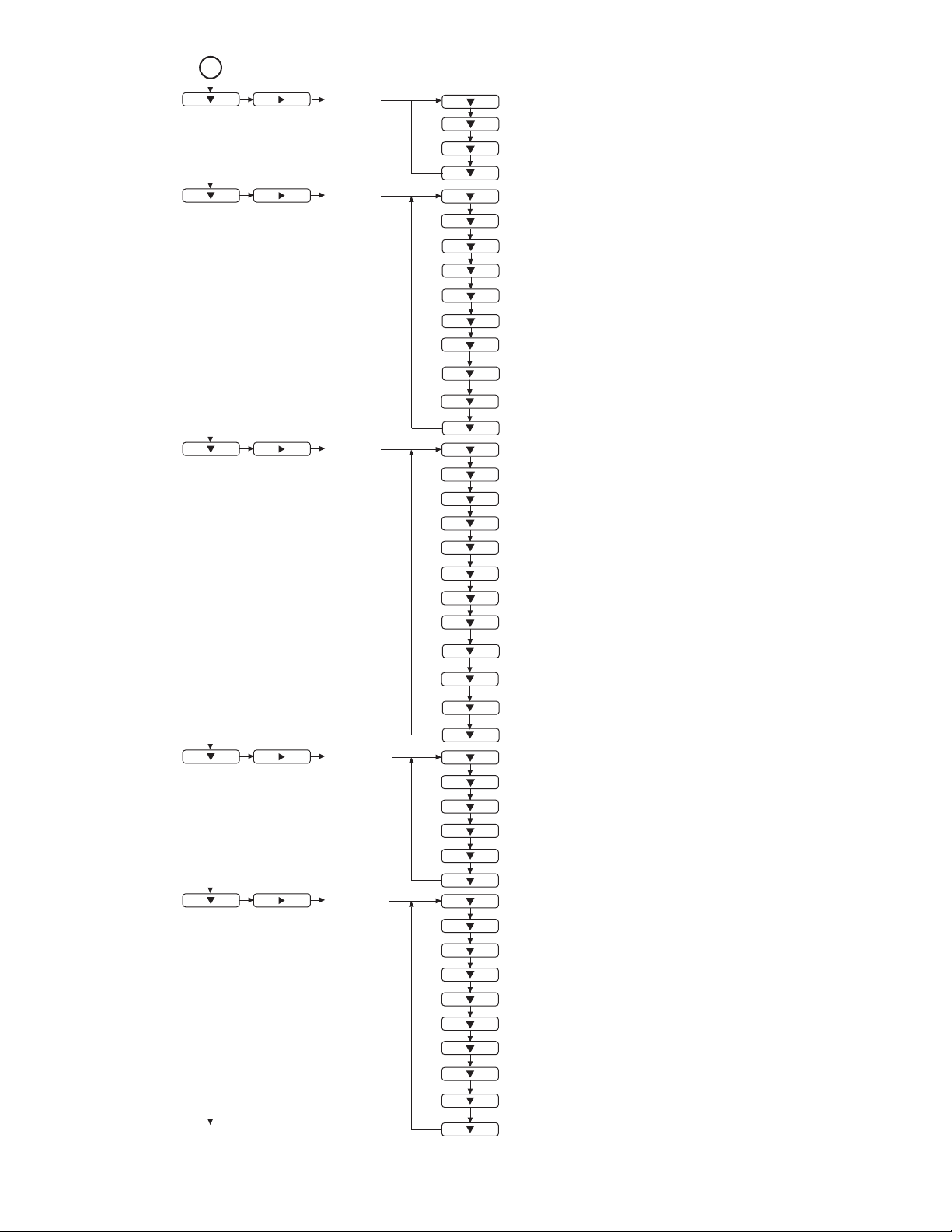
■ Power control/Input mode selection
Function Command Direction Parameter Reply Control/Response contents *
POWER CONTROL POWR W 0 Switches to standby mode. o
1 Returns from standby mode.
R 0 Standby mode
1 Normal mode
2 Input signal waiting mode
INPUT MODE SELECTION INPS W 0 Toggle change for input mode
1 PC1 DIGITAL
2PC2 ANALOG
3 AV2 COMPONENT
4 AV3 VIDEO
6PC3 ANALOG
7AV1 DIGITAL
R 1 PC1 DIGITAL
2PC2 ANALOG
3 AV2 COMPONENT
4 AV3 VIDEO
6PC3 ANALOG
7AV1 DIGITAL
Terminals not selected in DVI SELECT/BNC
SELECT cannot be selected.
“ERR” when AV (DIGITAL) is selected for DVI
SELECT.
“ERR” when PC (ANALOG) is selected for BNC
SELECT.
“ERR” when AV (COMPONENT) is selected for BNC
SELECT.
“ERR” when PC (DIGITAL) is selected for DVI
SELECT.
o
■ SCREEN menu (PC2/PC3)
Function Command
AUTO ASNC W 1
CLOCK CLCK WR 0-255 0-255
PHASE PHSE WR 0-63 0-63
POSITIONING POSITION OF
THE LONGEST
DIRECTION
POSITION OF
THE SHORTEST
DIRECTION
RESET ARST W 1
HPOS WR 0-500 0-500 A maximum value depends on a resolution.
VPOS WR 0-100 0-100
Direc-
PN-525U CONNECTION, ADJUSTMENT, OPERATION, AND FUNCTION
Parameter Reply Control/Response contents *
tion
2 – 13
-
-
-
Page 22
■ PICTURE menu
Function Command
AUTO AGIN W 1 When the input mode is PC2, PC3.
CONTRAST CONT WR 0-60 0-60 0-127 on PC2/PC3. o
BLACK LEVEL BLVL WR 0-60 0-60 0-127 on PC2/PC3.
TINT TINT WR 0-60 0-60 When the input mode is AV.
COLOR COLR WR 0-60 0-60
SHARPNESS SHRP WR 0-24 0-24
ADVANCED FLESH TONE FLES WR 0-2 0-2 0: OFF, 1: LOW, 2: HIGH o
3D-NR TDNR WR 0-2 0-2 0: OFF, 1: LOW, 2: HIGH
MPEG-NR MPNR WR 0-1 0-1 0: OFF, 1: ON
3D-Y/C YCSP WR 0-1 0-1 0: OFF, 1: ON
COLOR MODE BMOD WR 0 0 STD o
WHITE
BALANCE
GAMMA GAMM WR 0-2 0-2 0: 1.8, 1: 2.2, 2: 2.4 o
RESET ARST W 2
THRU CTMP WR 0 0 When the input mode is PC1. o
PRESET 1-15 1-15 From 1: approximately 3,000K to 15: approximately
USER 99 99
R-CONTRAST CRTR WR 0-512 0-512 “ERR” when CTMP is not set to 99.
R-CONTRAST CRTG WR 0-512 0-512
B-CONTRAST CRTB WR 0-512 0-512
Direc-
tion
Parameter Reply Control/Response contents *
2 2 VIVID
3 3 sRGB (When the input mode is PC)
10,000K
(500K steps)
-
-
■ AUDIO menu
Function Command
TREBLE AUTR WR
BASS AUBS WR
BALANCE AUBL WR
RESET ARST W 3
Direc-
tion
Parameter Reply Control/Response contents *
−10-10 −10-10 o
−10-10 −10-10
−10-10 −10-10
■ SETUP menu
Function Command
SCREEN MOTION SCSV WR 0-4 0-4 0: OFF, 1-4: PATTERN 1-4 o
MOTION TIME 1 MTIM WR 0-20 0-20 o
MOTION TIME 2 PATTERN 1 MINT WR 10-990 10-990 Per 10 seconds o
PATTERN 2-4 MINT WR 5-20 5-20 Per second
MONITOR STDR WR 0-1 0-1 0: LANDSCAPE, 1: PORTRAIT o
LANGUAGE LANG WR 14 14 ENGLISH o
Direc-
tion
Parameter Reply Control/Response contents *
1 1 DEUTSCH
22FRANÇAIS
33ITALIANO
44ESPAÑOL
55
66
日本語
-
PN-525U CONNECTION, ADJUSTMENT, OPERATION, AND FUNCTION
2 – 14
Page 23
Function Command
ID NUMBER ID NO. SETTING IDST W 0-255 Sets the monitor’s ID number. (“0” means “no ID num-
ID NO. SETTING
(ONCE)
ID NO. SETTING
(SUBSEQUENT)
ID CHECK IDCK W 0 ID: xxx
PICTURE FLIP PFIL WR 0-3 0-3 0: OFF, 1: MIRROR, 2: UPSIDE DOWN, 3: ROTATE o
Power On Delay PWOD WR 0 0 OFF o
IDSL W 1-255 Sets a monitor ID number.
IDLK W 1-255 Sets a monitor ID number.
Direc-
Parameter Reply Control/Response contents *
tion
ber”.)
R 0-255 Returns the monitor’s ID number.
This ID number is only effective for the command
immediately after this command.
0 Clears the ID number if one has been designated.
This ID number is effective for the next and all subsequent commands after this command.
0 Clears the ID number if one has been designated.
Displays monitor's own ID number and the selected
IDLK: yyy
1-60 1-60 ON
ID number on the screen.
■ OPTION menu
o
o
o
o
Function Command
DATE/TIME SETTING DATE WR AABBCCD-
SCHEDULE SC01~
DVI SELECT DVSL WR 0-1 0-1 0: PC (DIGITAL), 1: AV (DIGITAL) o
BNC SELECT BNSL WR 0-1 0-1 0: PC (ANALOG), 1: AV (COMPONENT) o
QUICK SHOOT (PC) QSPC WR 0-1 0-1 0: OFF, 1: ON o
QUICK SHOOT (AV) QSAV WR 0-1 0-1 0: OFF, 1: ON o
COLOR SYSTEM CSYS WR 0-5 0-5 0: AUTO, 1: PAL, 2: PAL-60, 3: SECAM, 4: NTSC3.58,
AUDIO OUTPUT AOUT WR 0-1 0-1 0: VARIABLE, 1: FIXED o
INPUT RESOLU-
TION (PC)
INPUT RESOLUTION (AV)
SELF ADJUST AADJ WR 0-1 0-1 0: OFF, 1: ON o
POWER MANAGEMENT PMNG WR 0-1 0-1 0: OFF, 1: ON o
RESOLUTION
CHECK
PIXEL SETTING
(PC2, PC3)
RESOLUTION
CHECK
C08
PXCK R
PXSL WR 1 1 V: 768) 1360 × 768
RESO R
Direc-
WR ABCDEF-
Parameter Reply Control/Response contents *
tion
DEE
FGGH
2 2 V: 768) 1280
3 3 V: 768) 1024
5 5 V: 480) 848
6 6 V: 480) 640
AABBCCDDEE
ABCD-
EFFGG
H
-
-
AA: Year, BB: Month, CC: Day, DD: Time, EE: Minute o
Schedule of a specified number
=
A: Schedule 0
B: Power 0
C: Day of the week 1 0
D: Day of the week 2 0
E: Day of the week 3 0
F: Time 00-23
G: Minute 00-59
H: Input 0
5: NTSC4.43
Returns current resolution in the form of hhh, vvv.
Not effective, 1 = Effective
= OFF, 1 = ON
= Only once,
= Every week,
1
= Every day
2
= Sunday,
= Monday through
1
= Saturday, 9 = Not exist
6
= Sunday,
= Monday through
1
= Saturday, 9 = Not exist
6
= Not specified,
= PC1/AV1, 2 = PC2,
1
= PC3/AV2, 4 = AV3
3
-
× 768
× 768
× 480
× 480
480i, 480p, 1080i, 720p, 1080p, VGA, etc.
-
o
PN-525U CONNECTION, ADJUSTMENT, OPERATION, AND FUNCTION
2 – 15
Page 24
Function Command
AUTO INPUT CHANGE AINC WR 0-1 0-1 0: OFF, 1: ON o
Direc-
tion
Parameter Reply Control/Response contents *
■ ENLARGE menu (When the input mode is PC)
Function Command
ENLARGE MODE EMAG WR 0-4 0-4 0: OFF, 1: 2
BEZEL WIDTH WIDT H OF THE
IMAGE POSITION (2
IMAGE POSITION (3
IMAGE POSITION (4
IMAGE POSITION (5
ENLARGED
SCREEN
POSITIONING
ENLARGE/IMAGE POSITION
SETTING
SHORTER SIDE
WIDTH OF THE
LONGER SIDE
× 2) EPOS WR 0-3 0-3 Refer to “■ Enlarge”
× 3) EPOS WR 0-8 0-8
× 4) EPOS WR 0-15 0-15
× 5) EPOS WR 0-24 0-24
THE LONGEST
DIRECTION
THE SHORTEST
DIRECTION
BEZH WR 0-100 0-100
BEZV WR 0-100 0-100
EPSH WR -999-999 -999-999 The setting range depends on the ENLARGE MODE
EPSV WR -999-999 -999-999
ESTG WR XXYY XXYY XX: Enlarge mode (Same as EMAG),
Direc-
tion
Parameter Reply Control/Response contents *
× 2, 2: 3 × 3, 3: 4 × 4, 4: 5 × 5
setting and the IMAGE POSITION.
YY: Image Position (Same as EPOS)
■ PIP/PbyP menu
Function Command
PIP MODES MWIN WR 0-3 0-3 0: OFF, 1: PIP, 2: PbyP, 3: PbyP2 o
PIP SIZE MPSZ WR 1-12 1-12 o
PIP POS T H E L O N G E S T
DIRECTION
THE SHORTEST
DIRECTION
PIP V/H-POS MPOS W 0-100,
PIP BLEND MWBL WR 0-15 0-15 o
PIP SOURCE MWIP WR 1 1 PC1 DIGITAL o
SOUND CHANGE MWAD WR 1-2 1-2 1: MAIN, 2: SUB o
MAIN POS (Main screen) MWPP WR 0-1 0-1 0: POS1, 1: POS2 o
PbyP2 POS (Sub screen) MW2P WR 0-2 0-2 0: POS1, 1: POS2, 2: POS3 o
AUTO OFF MOFF WR 0-1 0-1 0: MANUAL, 1: AUTO o
MHPS W 0-100 o
MVPS W 0-100 o
Direc-
Parameter Reply Control/Response contents *
tion
R 0-100 o
R 0-100 o
0-100
R 0-100,
0-100
2 2 PC2 ANALOG
33AV2 COMPONENT
44AV3 VIDEO
6 6 PC3 ANALOG
7 7 AV1 DIGITAL
Specify the position in MPOSxxxyyy format.
(xxx: Longer side, yyy: Shorter side position)
Returns a response in (xxx,yyy) format.
(xxx: Longer side, yyy: Shorter side position)
-
o
o
■ Initialization/Functional Restriction Setting (FUNCTION) menu
Function Command
ALL RESET RSET W 0
ADJUSTMENT
LOCK
OSD DISPLAY LOSD WR 0-1 0-1 0: ON, 1: OFF o
LED OFLD WR 0-1 0-1 0: ON, 1: OFF o
ALCK WR 0-2 0-2 0: OFF o
Direc-
tion
Parameter Reply Control/Response contents *
PN-525U CONNECTION, ADJUSTMENT, OPERATION, AND FUNCTION
2 – 16
-
Page 25
■ Others
Function Command
SCREEN SIZE (PC) WIDE WR 1-5 1-5 1: WIDE, 2: NORMAL, 3: DotbyDot, 4: ZOOM1,
SCREEN SIZE (AV) WIDE WR 1-5 1-5 1: WIDE, 2: ZOOM1, 3: ZOOM2, 4: NORMAL,
VOLUME VOLM WR 0-31 0-31 o
MUTE MUTE WR 0-1 0-1 0: OFF, 1: ON
INFORMATION MODEL INF1 R Value o
SERIAL NO SRNO R Value o
BRIGHT VLMP WR 0-31 0-31 Brightness o
TEMPERATURE SENSOR DSTA R 0 Internal temperature normal o
TEMPERATURE ACQUISITION ERRT R Value Temperature at temperature sensors 1 through 3 are
CAUSE OF LAST STANDBY MODE STCA W 0 Initialization o
Direc-
Parameter Reply Control/Response contents *
tion
5: ZOOM2
5: DotbyDot
1 Internal temperature abnormal (Standby mode) o
2 Internal temperature abnormal (Temperature is nor-
mal now, but it was abnormal during operation.)
3 Internal temperature abnormal
(Brightness of the backlight decreases.)
4 Temperature sensor abnormal o
returned in the following forms:
[Sensor 1], [Sensor 2], [Sensor 3]
R 0 No detectable error has occurred
1 Standby mode by POWER button
2 Main power “OFF” by the main power switch
3 Standby mode by RS-232C
4 Waiting mode by No Signal
(Incl: VESA DPMS/DMPM)
6 Standby mode by abnormal temperature
8 Standby mode by SCHEDULE setting
o
o
-
o
o
o
PN-525U CONNECTION, ADJUSTMENT, OPERATION, AND FUNCTION
2 – 17
Page 26
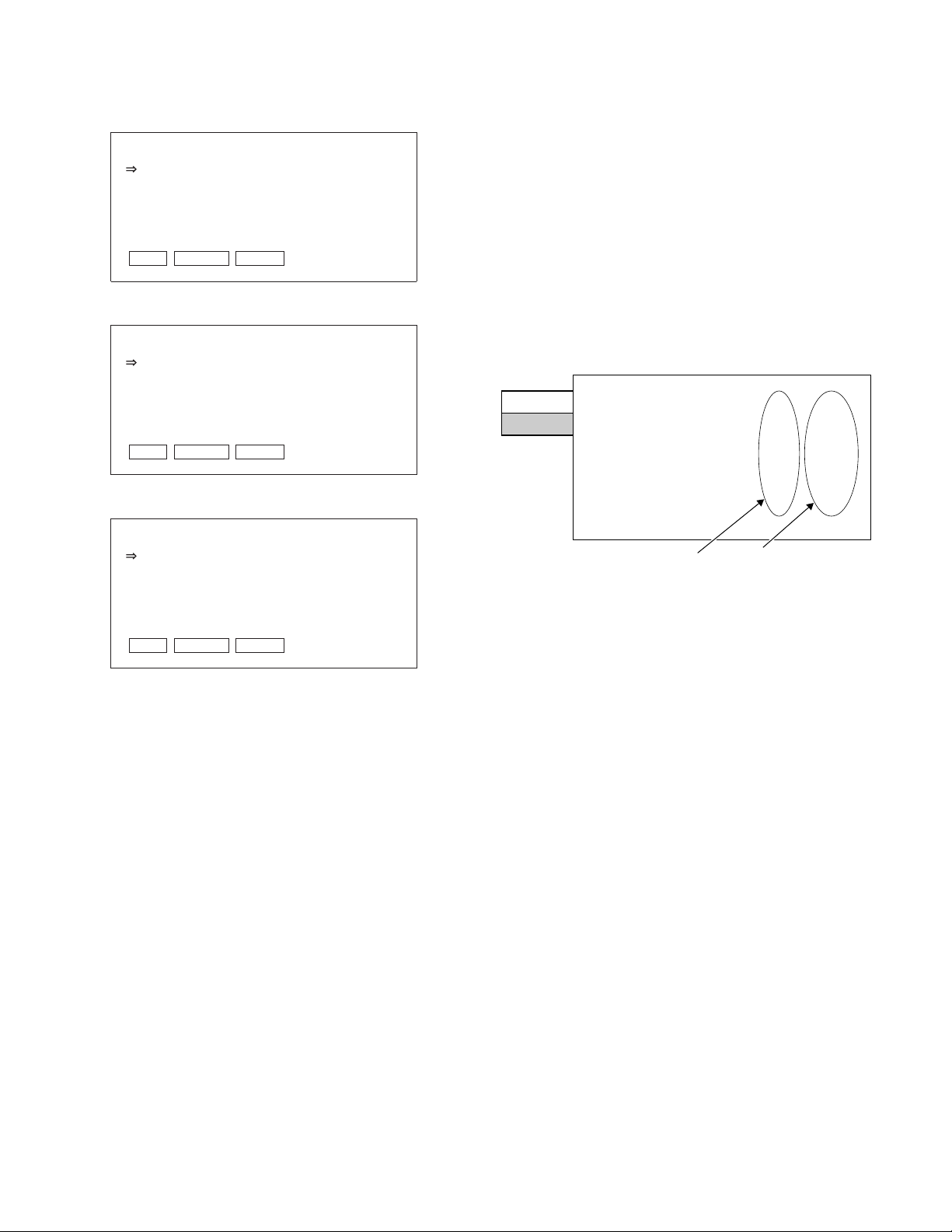
3. SERVICE MENU
g
SERVICE MENU 1:
Used to display the model name, the manufacturing No., the firmware
version/checksum, and the usage time.
[Operating procedures]
1) Press [SIZE] button for 5sec, and press [1] [ 4 ] [3] [ 2 ] buttons in
this sequence. “SERVICE MENU1” is displayed.
Firmware checksum
Firmware version
Serial number
Model name
SERVICE1
SERVICE2
SERVICE MENU1 1/1
MODEL
S/N
FIRM VERSION
CHECK SUM
USAGE TIME
WHITE BALANCE CHECK
CALIBRATION CHECK
㧦
PNXXXXX
㧦
㧦
XXXXX (XXXXXXXX)
㧦
OK
㧦
XXXXXH
㧦
XXXXXXXX
XXXX
㧦
PC AV
PC2 PC3 AV2 AV3N AV3P
END[MENU]
Use time
• PC2/PC3/SOG SYNC THRESHOLD LEVEL :
Do not change the setting.
• HARDWARE CHECK SETTING:
Do not change the setting.
• AUTO INPUT CHANGE DELAY :
Do not change the setting.
[Operating procedures]
1) With “SERVICE MENU1” displayed, select “SERVICE2” with [ 4 ]
button and press [3] button.
SERVICE MENU2 1/2
SERVICE1
SERVICE2
ʋ
AGING
CALIBRATION
FACTORY RESET
MODEL TYPE
HARDWARE CHECK
WHITE BALANCE SETTING
COMPONENT PHASE
=>
=>
=>
< XX >
=>
=>
=>
When the calibration set value becomes the default
value, it is displayed.
(It is not displayed usually.)
When the white balance set value becomes the default
value by replacement of the PWB or the panel, it is
displayed.
(It is not displayed usually.)
*Immediately after turning on the power, “CALCULATING” is displayed
for the checksum for a while, and the result is dipslayed.
SERVICE MENU 2:
• AGING:
AGING. Refer to “3-1. AGING”.
• CALIBRATION :
Used to adjust automatically the gain and the offset of PC/components/composite. Refer to “3-2. Calibration”.
• FACTORY RESET :
Used to reset the user adjustment values, the usage time, and the
operation logs to the factory setting. Refer to “3-3. FACTORY
RESET”.
• MODEL TYPE :
Used to select the destination. JP: Japanese model, US: North America model, EU: A European model
After changing the MODEL TYPE, execute ALL RESET.
(Refer to “2-2. INITIALIZATION (RESET)/FUNCTIONAL RESTRICTION SETTING”)
• HARDWARE CHECK :
Used to display the hardware detection result. Refer to “3-4. HARDWARE CHECK”.
• WHITE BALANCE SETTING:
Refer to “3-5. WHITE BALANCE SETTING”.
• COMPONENT PHASE :
Do not change the setting.
2) Select setting item with [ 2 ] [ 4 ] button.
3) Adjust it with the [1] [3] button.
When the item with => mark press [3] button and advances to the
next screen.
4) Press [MENU] button to return to the previous screen sequentially,
terminating the operation.
3-1. AGING
(1) Operating procedures
1) Enter the “SERVICE MENU 2” mode.
2) Select [AGING] with [ 2 ] [ 4 ] buttons, and press [3] button.
3) Select [AGING1] or [AGING2] with [ 2 ] [ 4 ] buttons, and press [3]
button. The aging is started.
AGING1: Every time when [3] button is pressed, the whole screen
color is changed.
Dark
Dark
blue
green
AGING2: The whole screen color is changed every 2 sec.
Dark
Dark
blue
4) To terminate aging, turn off the main power source. (The power button of the remote controller or the machine cannot terminate aging.)
*AGING3 must not be used.
reen
Dark
red
Dark
red
Blue Green Red White Black
Blue Green Red White Black
PN-525U CONNECTION, ADJUSTMENT, OPERATION, AND FUNCTION
2 – 18
Page 27
3-2. CALIBRATION
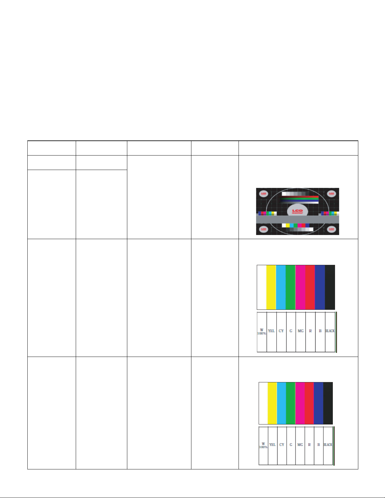
Adjusts the offset and the gain of an A/D converter by the following input mode.
• PC2 ANALOG mode (D-sub terminal)
• PC3 ANALOG mode (BNC terminal)
• AV2 COMPONENT mode (component terminal)
• AV3 VIDEO mode (composite terminal)
(1) Operating procedures
1) Select the input mode to be adjusted with [INPUT] button.
2) The video signal for adjustment is displayed on the screen.
Note:
• Be sure to use the following video signal to perform the adjustment.
• Since PC2 ANALOG (D-sub terminal) and PC3 ANALOG (BNC terminal) differ in the calibration results, be sure to adjust them with their own
input mode.
Input mode Signal type
PC2 ANALOG PC ANALOG signal
(D-sub terminal)
PC3 ANALOG PC ANALOG signal
(BNC terminal)
AV2 COMPONENT COMPONENT signal Y level: 0.7 Vp-p
Input signal level (Adjusted
standard value)
RGB level: 0.7 Vp-p 1920x1080 60Hz
(Pedestal to white level)
Pb/Pr level: 0.7 Vp-p
signal timing Input image
or
XGA (1024x768)
60Hz
1080i 60Hz Full color bar (White 100%, color saturation 100%)
The adjustment image displayed by executing
“Adj_uty.exe” in the CD-ROM packed together with
the product.
(Or a video image with 0 to 255 gradations of RGB
White)
*Recommended signal generator:
VG-849, VG-859 made by Astro Design.
AV3 VIDEO VIDEO (NTSC3.58)
signal
0.714 Vp-p
(Pedestal to white level)
PN-525U CONNECTION, ADJUSTMENT, OPERATION, AND FUNCTION
NTSC3.58 Full color bar (White 100%, color saturation 100%)
2 – 19
*Recommended signal generator:
VG-849, VG-859 made by Astro Design.
Page 28
3) Enter the “SERVICE MENU 2” mode.
4) Select [CALIBRATION] with [ 2 ] [ 4 ] buttons, and press [3] button. The CALIBRATION screen is displayed.
• CALIBRATION screen when PC2/PC3 ANALOG mode
CALIBRATION PC (ANALOG)
AUTO CALIBRATION
ADC OFFSET1 R: 511 B:G: 511 511
ADC OFFSET2 R: 128 G : B:128 128
ADC GAIN R : 511 511 511G: B:
This machine is provided with the function to watch for any abnormality
in the hardware.
When an abnormality occurs in the hardware (internal power voltage,
backlight, temperature), “SERVICE CALL” message is displayed on the
screen. The power lamp flashes in red.
When only a temperature abnormality occurs, “TEMPERATURE” message is displayed on the screen. The power lamp flashes in red and
green alternately.
The abnormal position can be located by two methods below.
OK CANCEL RESET
• CALIBRATION screen when AV2 COMPONENT mode
CALIBRATION COMPONENT
AUTO CALIBRATION
ADC OFFSET1 Y : 511 Cr :Cb: 511 511
ADC OFFSET2 Y : 128 Cb : Cr :128 128
ADC GAIN Y : 511 511 511Cb: Cr :
OK CANCEL RESET
• CALIBRATION screen when AV3 VIDEO mode
CALIBRATION COMPONENT
AUTO CALIBRATION
ADC OFFSET1 : 511
ADC OFFSET2 : 128
ADC GAIN : 511
OK CANCEL RESET
5) Select [AUTO CALIBRATION] with [ 2 ] and [ 4 ] buttons and press
[3] button. The calibration is executed and the data are saved to
the EEPROM.
The adjustment result is displayed on the ADC OFFSET1/ADC
OFFSET2/ADC GAIN items.
6) Select [OK] with [ 2 ] [ 4 ] buttons, and press [MENU] button. The
CALIBRATION screen is closed.
3-3. FACTORY RESET
Resets the user adjustment value, USAGE TIME and the Operation log
to the factory preset values.
(Note)
When resetting is made, the operation logs are also deleted. If necessary, save the operation logs before resetting.
1) Display the SERVICE MENU 2.
2) Select “FACTORY RESET” with [ 2 ] [ 4 ] button, and press [3] button.
3) Select [ON] with [1] [3] buttons, and press MENU button.
“RESETTING” is displayed. After completion of initialization, the unit
is booted in the PC1 (digital) mode.
4) Turn the main power switch off and then back on.
[Method 1]
<Operating procedure>
1) SERVICE MENU 2 is displayed.
2) Select “HARDWARE CHECK” with [ 2 ][ 4 ] buttons, and press [3]
button. “HARDWARE CHECK” menu is displayed.
HARDWARE CHECK
SERVICE1
SERVICE2
LCD 12V : OK XXX
OK XXXVIDEO 5V :
OK XXXAMP 3.3V :
OK XXXAMP 9V :
OK XXXBACKLIGHT :
OK XXXTHERMAL1 :
OK XXXTHERMAL2 :
OK XXXTHERMAL3 :
OK...[MENU]
Watch result
3) The watch result and the current measurement value of the hardware are displayed.
• Watch result: OK or NG is displayed.
After turning ON the main power, if an abnormality occurs to be NG once, the NG state is
kept until the main power is turned OFF.
• Measurement value: The measurement value at the time when
HARDWARE CHECK menu is displayed is
displayed.
The measurement value at the time when an
abnormality occurred is saved in the log data.
*The measurement value of the internal voltage displayed is the A/D
conversion value. The normal range is as shown below.
LCD 12V : Measurement value 174~190
VIDEO 5V : Measurement value 171~208
AMP 3.3V : Measurement value 187~213
AMP 9V : Measurement value 173~190
4) For the countermeasures against NG positions, refer to “7. Hardware check NG” in “CHAPTER 5. TROUBLESHOOTING.”
5) Press MENU button to return to the previous screen, and terminate
the operation.
[Method 2]
<Operating procedure>
Measurement value
3-4. HARDWARE CHECK OPERATION
PROCEDURES
PN-525U CONNECTION, ADJUSTMENT, OPERATION, AND FUNCTION
1) Send “HTST0000” that is 232C command.
2) Result is returned.
2 – 20
Page 29
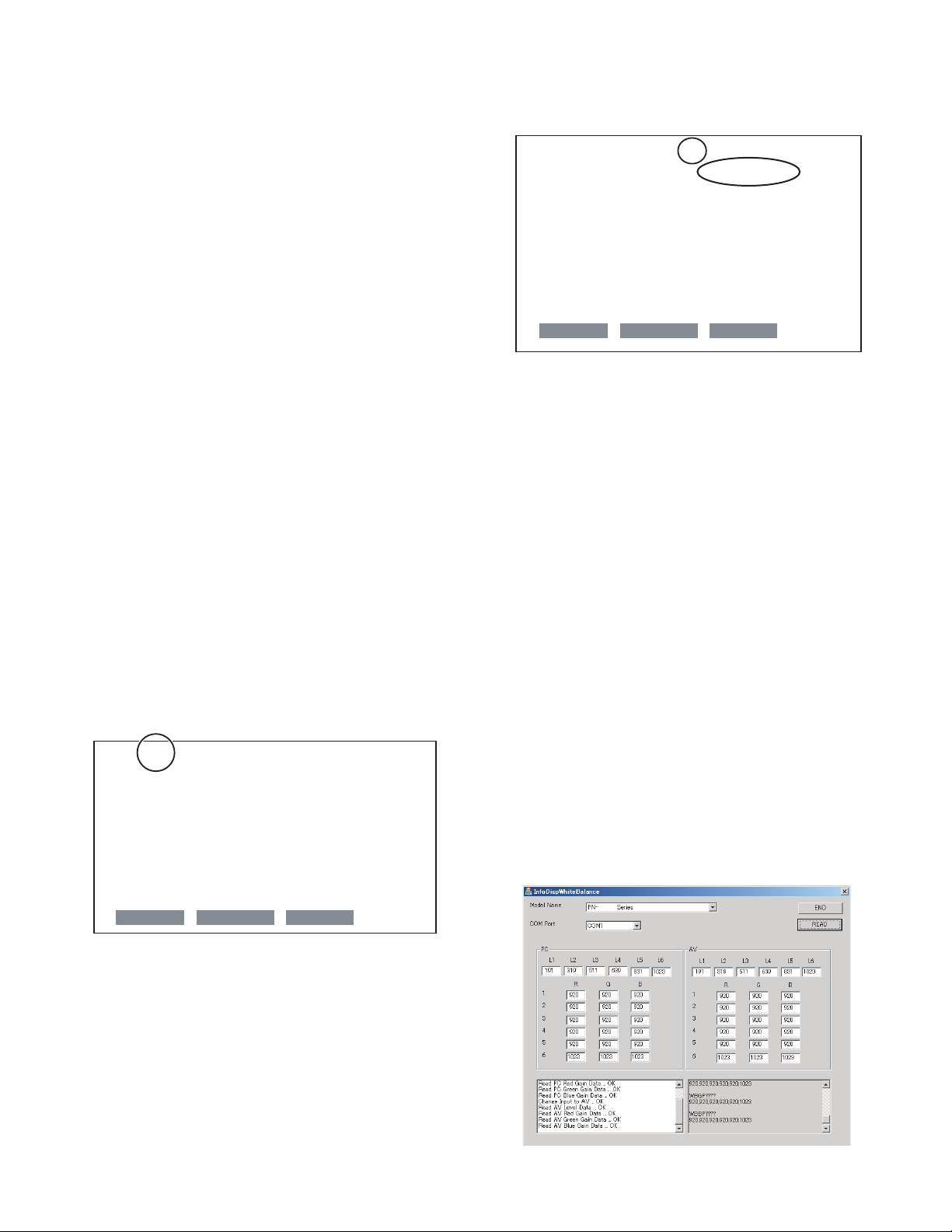
3-5. WHITE BALANCE SETTING PROCEDURES
(1) Outline
The white balance setting is used to correct shade variations in each
panel. When the panel is not changed, take over the panel setting to
suppress variations. When the panel is changed, perform resetting to
set the standard state.
(2) When replacing the PWB (when the panel is not
changed)
(2)-1. White Balance setting information read
The White Balance setting information of the information display before
replacement is read. There are two methods to read the White Balance
setting information as follows.
• Method 1: The setting information is read from the SERVICE MENU.
• Method 2: Use the White Balance setting read tool.
Use either way to read the White Balance setting information.
Since the white balance is set in the PC system input mode, read the
setting information in the PC system input mode.
[Method 1]
The setting information is read from the SERVICE MENU.
[Operating procedures]
1) Select the PC system input mode with [INPUT] button.
• Select one of PC1 DIGITAL, PC2 ANALOG, and PC3 ANALOG
modes.
2) Any image is displayed on the screen.
3) SERVICE MENU2 is displayed.
4) Select “WHITE BALANCE SETTING” with [ 2 ] [ 4 ] buttons, and
press [3] button.
The WHITE BALANCE SETTING menu is displayed.
“(PC)” is displayed on the title column.
5) Check to confirm that the PATTERN item is “9000K”.
If it is “6500K”, use [ 2 ] [ 4 ] buttons to select “PATTERN” and use
[3] button to select “9000K.”
6) Use [ 2 ] [ 4 ] buttons to select “LEVEL” and press [3] button. The
LEVEL menu is displayed.
LEVEL (PC)
LEVEL1
LEVEL2
LEVEL3
LEVEL4
LEVEL5
LEVEL6
OK CANCEL RESET
< 191 >
< 319 >
< 511 >
< 639 >
< 831 >
< 1023 >
10) Select “CANCEL” with [ 2 ] [ 4 ] [1] [3] buttons and press [MENU]
button.
The WHITE BALANCE SETTING menu is terminated.
WHITE BALANCE SETTING (PC)
PATTERN
LEVEL =>
L1 R: 920 G: 920 B: 920
L2 R: 920 G: 920 B: 920
L3 R: 920 G: 920 B: 920
L4 R: 920 G: 920 B: 920
L5 R: 920 G: 920 B: 920
L6 R: 1023 G: 1023 B: 1023
OK CANCEL RESET
< 9000 K >
[Method 2]
Use the White Balance setting read tool.
For detailed operation procedures of the tool, refer to the separate
sheet (3-6. WHITEBALANCE SETTING READ TOOL OPERATING
PROCEDURE).
[Operating procedures]
1) Connect the information display and the PC with the RS-232C
straight cable.
2) Boot the tool, “InfoDispWhiteBalance.exe”.
3) Turn ON the power of the information display.
4) Press [READ] button of the tool.
5) After normal completion of reading data, check to confirm that the
setting information of L1 - L6 on the PC side is as shown in the figure below.
If the setting information differs, the setting information cannot be
taken over. Refer to “(3) When replacing the panel or when the old
PWB does not operate” to reset the setting information to the
default values. (Unless a change is made individually, these procedures are not required in normal cases.)
6) Write down the setting values of 1 - 6 of R/G/B on the PC side.
(Refer to the figure below.)
* Though the setting values of the AV input system are read too,
since only the setting values of the PC system input are used,
write down only the setting values of the PC system input.
XXXXX
7) Check to confirm that the setting information is same as the above
display.
If the setting information differs from the above display, the setting
information cannot be taken over. Refer to “(3) When replacing the
panel or when the old PWB does not operate” to reset the setting
information to the default values. (Unless a change is made individually, these procedures are not required in normal cases.)
8) Select “CANCEL” with [ 2 ] [ 4 ] [1] [3] buttons and press [MENU]
button.
The display returns to the WHITE BALANCE SETTING menu.
9) Write down all the displayed set values of R, G, and B in L1 - L6.
PN-525U CONNECTION, ADJUSTMENT, OPERATION, AND FUNCTION
2 – 21
Page 30

(2)-2. White Balance setting value write
After replacement of the PWB, perform the following procedures to write
the setting information of the white balance. When setting is made in the
PC system input mode, it is automatically reflected on the AV system
input side. Therefore, be sure to write the white balance setting information in the PC system input mode.
[Operating procedures]
1) Select the PC system input mode with [INPUT] button.
• Select one of PC1 DIGITAL, PC2 ANALOG, and PC3 ANALOG
modes.
2) Any image is displayed on the screen.
3) SERVICE MENU2 is displayed.
4) Select “WHITE BALANCE SETTING” with [ 2 ] [ 4 ] buttons, and
press [3] button.
The WHITE BALANCE SETTING menu is displayed.
“(PC)” is displayed on the title column.
5) Check to confirm that the PATTERN is “9000K”.
If it is “6500K”, select “PATTERN” with [ 2 ] [ 4 ] buttons and press
[3] button to set to “9000K”.
6) Select “LEVEL” with [ 2 ] [ 4 ] buttons and press [3] button. The
LEVEL menu is displayed.
7) Select “RESET” with [ 2 ] [ 4 ] [1] [3] buttons, and press [MENU]
button.
8) Select “OK” with [1] [3] buttons, and press [MENU] button. The
setting is saved and the screen returns to the WHITE BALANCE
SETTING menu.
9) Set the values L1 - L6 of R, L1 - L6 of G, and L1 - L6 of B to the values previously written down. Select L1 - L6 with [ 2 ] [ 4 ] buttons,
select R/G/B with [1] [3] buttons, and adjust the set values with
[ 2 ] [ 4 ] buttons.
10) Select “L*” at the left end with [1] [3] buttons, and repeat the
operation.
11) Select “OK” with [ 2 ] [ 4 ] buttons, and press [MENU] button.
The set data are saved and the WHITE BALANCE SETTING menu
is terminated.
12) Check to confirm that all the set values are set properly.
13) Read the set data of WHITE BALANCE and check to confirm that
all the values are properly set.
(3) When replacing the panel or when an old PWB does not
operate
When the white balance setting information is reset in the PC system
input mode, the setting information of the AV system input mode is
reset, too. Therefore, be sure to reset in the PC system input mode.
[Operating procedures]
1) Select the PC system input mode with [INPUT] button.
• Select one of PC1 DIGITAL, PC2 ANALOG, and PC3 ANALOG
modes.
2) Any image is displayed on the screen.
3) SERVICE MENU2 is displayed.
4) Select “WHITE BALANCE SETTING” with [ 2 ] [ 4 ] buttons, and
press [3] button.
The WHITE BALANCE SETTING menu is displayed.
“(PC)” is displayed on the title column.
5) Check to confirm that the PATTERN is “9000K”.
If it is “6500K”, select “PATTERN” with [ 2 ] [ 4 ] buttons and press
[3] button to set to “9000K”.
6) Select “LEVEL” with [ 2 ] [ 4 ] buttons and press [3] button. The
LEVEL menu is displayed.
7) Select “RESET” with [ 2 ] [ 4 ] [1] [3] buttons and press [MENU]
button.
8) Check to confirm that the set value is changed as shown below.
• Initial values of the PC system input mode
LEVEL (PC)
LEVEL1
LEVEL2
LEVEL3
LEVEL4
LEVEL5
LEVEL6
OK CANCEL RESET
< 191 >
< 319 >
< 511 >
< 639 >
< 831 >
< 1023 >
9) Select “OK” with [1] [3] buttons, and press [MENU] button.
The display returns to the WHITE BALANCE SETTING menu.
10) Select “RESET” with [ 2 ] [ 4 ] [1] [3] buttons and press [MENU]
button.
11) Check to confirm that all the set value is changed as shown below.
• Initial values of the PC system input mode
WHITE BALANCE SETTING (PC)
PATTERN
LEVEL =>
L1 R: 920 G: 920 B: 920
L2 R: 920 G: 920 B: 920
L3 R: 920 G: 920 B: 920
L4 R: 920 G: 920 B: 920
L5 R: 920 G: 920 B: 920
L6 R: 1023 G: 1023 B: 1023
OK CANCEL RESET
< 9000 K >
12) Select “OK” with [1] [3] buttons, and press [MENU] button.
The WHITE BALANCE SETTING menu is terminated.
13) Perform the WHITE BALANCE setting read procedures to check
that all settings have been properly changed.
PN-525U CONNECTION, ADJUSTMENT, OPERATION, AND FUNCTION
2 – 22
Page 31

3-6. WHITE BALANCE SETTING READ TOOL OPERATING PROCEDURE
(1) White Balance setting read tool operating conditions
The operating conditions of the White balance setting read tool of the
information display are as follows.
OS : Windows98SE, Windows2000, WindowsXP,
Communication port : RS-232C port recognized as a COM port
The required RS-232C cable is as shown below. Connect the PC’s
COM port and the RS-232C input terminal of the display.
RS-232C cable: Straight cable (D-Sub 9 pin female - female)
(2)
Installing the White Balance setting read tool
The White Balance setting read tool is provided as the compression file
of “PNXXXXX_InfoDispWhiteBalance.zip.”
Decompress “PNXXXXX_InfoDispWhiteBalance.zip,” and the execution file of “InfoDispWhiteBalance.exe” and “InfoDispWhiteBalance.ini”
is generates. Copy “InfoDispWhiteBalance.exe” and “InfoDispWhiteBalance.ini” to an optional directory and execute “InfoDispWhiteBalance.exe”.
(3)
White Balance setting read tool operating procedures
Windows Vista
(Which allows communication in 9600bps.)
tool.
When “OK” is indicated for all the items as shown below, data acquisition is successfully completed.
Power On … OK
Change Input to PC … OK
Read PC Level Data … OK
Read PC Red Gain Data … OK
Read PC Green Gain Data … OK
Read PC Blue Gain Data … OK
Change Input to AV … OK
Read AV Level Data … OK
Read AV Red Gain Data … OK
Read AV Green Gain Data … OK
Read AV Blue Gain Data … OK
• When “Power On ... NG” is displayed:
Check the power status of the connected information display.
When “READ” is executed in the power standby state, the operation
may fail sometimes. Turn ON the power, and press [READ] button
again to read the setting value.
• When “Command Sending Retry Error”, “Nothing Received” is
displayed:
Check to confirm that the PC and the information display are connected with a proper RS-232C cable.
• When “COM Port Open Error” is displayed:
Check to confirm that the COM port is not used by another tool. If the
COM port is used by another tool, terminate the tool and press
[READ] button again to read the setting value.
(4) White Balance setting read tool version check
To check the version of the White Balance setting read tool, display the
property of “InfoDispWhiteBalance.exe” and check the production version item.
The procedures to read the White Balance setting by using the White
Balance setting read tool are as follows:
1) Select “PNXXXXX Series” on the column of Model Name.
2) Select a COM port to be used on the column of COM port.
3) Turn on the power of the LCD monitor.
4) Press [READ] button.
5) When reading of all the setting items is completed, the set value is
displayed.
The data acquisition log is displayed on the left lower section of the
PN-525U CONNECTION, ADJUSTMENT, OPERATION, AND FUNCTION
2 – 23
Page 32

4. FIRMWARE UPDATE PROCEDURES
4-1.
OPERATING CONDITIONS OF FIRMWARE UPDATE
The operating conditions for firmware update of the information display
are as follows:
OS :
Communication port : RS-232C port recognized as a COM port
The RS-232C cable required for update is as follows. Connect the COM
port of PC and the RS-232C input terminal of the display with the cable.
RS-232C cable: Straight cable (D-Sub 9pin female - female)
Windows 98SE, Windows 2000, Windows XP,
Windows Vista
(Which allows communication in 115Kbps.)
• Installing folder specifying screen
Specify the installing folder as “C:\SHARP_PNxxxxx” (which is set as
the default and must not be changed), and press [Next] button.
• Program folder selection screen
4-2. INSTALLATION OF THE FIRMWARE UPDATER
The firmware updater is provided as a self-extract file of
“xxxxxFirmwareUpdater_yyy.exe”.
(“xxxxx” indicates the model name, and “yyy” the firmware version.
When “FirmwareUpdater.exe” is executed, a folder (C:\SHARP_PNxxxxx) is
made and the updater program and the firmware is installed to the folder.
• FirmwareUpdater.exe booting screen
Press [Next] button.
Press [Next] button.
• Shortcut making screen
Check “Create a shortcut on Desktop” and press [Next] button.
PN-525U CONNECTION, ADJUSTMENT, OPERATION, AND FUNCTION
2 – 24
Page 33

• Installing contents check
Check the contents of installation, and press [Next] button.
• Installation completion screen
4-3. FIRMWARE UPDATE
To update the firmware, click the icon of “SHARP PNxxxxx FirmwareUpdater” to boot the updater program, and follow the instructions on the
screen.
• COM port selection
After completion of installation, the installation completion screen is
displayed. Press [Finish] button.
Select the COM port to be used for communication.
(“COM1” on the above screen)
• Batch file setting
Set the batch file name as “C:\SHARP_PNxxxxx\isp_flash16_ext.txt”.
(It is set as the default. Do not change it.)
PN-525U CONNECTION, ADJUSTMENT, OPERATION, AND FUNCTION
2 – 25
Page 34
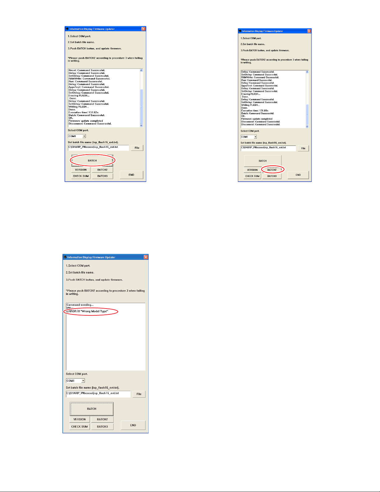
• Firmware update
• When updating is failed
Press [BATCH] button, and the firmware writing is started.
For about 3minutes and writing is completed. When “Firmware version
up completed” is displayed, the firmware update is completed.
The new version firmware can be operated by turning OFF and ON the
main power.
If beside this model is connected when the [BATCH] button is pressed,
[ERROR!!! “Wring Model Type”] message is displayed as shown below.
Check the connecting model.
First, turn OFF the main power and then turn it ON again. Then, press
[BATCH2] button to start writing the firmware.
In about 3minutes, updating is completed and “Firmware update completed” is displayed. It is the end of firmware updating.
After completion of firmware updating, turn OFF and ON the main
power, and the new version firmware is operated.
PN-525U CONNECTION, ADJUSTMENT, OPERATION, AND FUNCTION
2 – 26
Page 35

4-4. VERSION CHECK PROCEDURES
(1) Check method by the firmware updater
The current firmware version can be checked by pressing
[VERSION] button when the monitor power lamp is lighted in green.
The check sum can be also checked by pressing [CHECK SUM]
button similarly.
(2) Check method by the service menu
With an image displayed on the screen, use the remote controller to
display SERVICE MENU 1 and to check the firmware version.
PN-525U CONNECTION, ADJUSTMENT, OPERATION, AND FUNCTION
2 – 27
Page 36

5. EDID WRITING PROCEDURES
[Tool operating conditions]
• Windows 98SE/ Windows 2000/ Windows XP/ Windows Vista.
• The I/O address of the printer port must be set to 378.
(Refer to “Supplementary descriptions.”)
• When you use this model in Windows XP/ Windows Vista,
log in by manager authority.
[Installing procedures]
1) Make a folder of “c:\fg.”
2) Decompress the EDID writing tool for servicing, and copy all the
files to “c:\fg.”
If there is already a folder for the launcher tool, use the folder.
(Use the latest-version launcher tool.)
[Operating procedures]
1) Connect the jig to the PC.
2) Execute “c:\fg\launcher.exe.”
However, execute it according to the following procedures to run
launcher.exe when you use WindowsVista.
i). Open the copy folder by explorer and click the right mouse but-
ton to open menu on the “launcher.exe”, and select “Run as
administrator”.
3) The following screen is displayed.
Select PNXXXXX in the column of [Class].
Select [PNXXXXX write EDID (PC ANALOG/DIGITAL)] in
[Contents].
After selection, click [Go].
4) The window for checking the execution content is displayed. If it is
OK, press [YES], and if not, press [NO]. When [NO] is pressed, the
display returns to 3). When [YES] is pressed, the process goes on
to the next step.
ii). Select [Accept] in the “User Account Control” dialog to run
“launcher.exe”.
User Account Control
An unidentified program wants access to your computer
Don't run the program unless you know where it's from
or you've used it before.
launcher.exe
Unidentified Publisher
[Cancel]
I don't know where this program is from or what it's for.
[Allow]
I trust this program. I know where it's from or I've used it
before.
At that time, do not connect the monitor to the jig.
5) If the window below is displayed, check for the following.
1. The jig and the PC are not connected properly.
2. The jig and the monitor are already connected.
Check the connection and press [OK] and then [Next].
PN-525U CONNECTION, ADJUSTMENT, OPERATION, AND FUNCTION
2 – 28
Page 37

6)
When the following window is displayed, connect the monitor to the jig.
[Setting on the monitor side]
1: Connect the VGA cable and the DVI-D cable to the monitor and
the jig. (Refer to the connection diagram of the PNXXXXX EDID
writing tool.)
2: To cancel write-protect of EDID, press [INPUT] button of the
main unit and turn ON the main power of the monitor at the
same time and wait until [No Signal] is displayed.
*If write-protect cannot be canceled by [INPUT] button, send the
serial command of “EDWP1230.”
(Refer to “Canceling write-protect of EDID by the serial command.”)
7) Click [Start] button.
8) The window below is displayed.
[Supplementary descriptions]
• Setting the printer port I/O address to 378
1. Open the system of the control panel.
2. Open the hardware tag, and click the device manager button.
3. Click “+” mark on the left of “Port (COM/LPT)”
Check to confirm that there is “ECP printer port (LPT1).”
Open the property of the printer port (LPT1), and open the resource
4.
5. Uncheck “Use automatic settings” and select “Basic setting 0000.”
(If “I/O range” is already “0378 - 037F,” there is no need to change.)
tag.
On the above screen EDID is written and verified. If the operation is
interrupted before completion, the connection may be improper.
Check for it. After completion of writing, the window of 6) is displayed.
Then connect the monitor to the jig.
Repeat EDID writing to the next monitor from 6).
9) In case of an error occurs in writing or verifying
If an error occurs in writing or verifying, the above window is displayed.
When [Retry] button is pressed, EDID writing and verifying are performed again. Check the connection between the monitor and the
PC, cancel write-protect again, and repeat the procedures from 1).
10) When writing is normally completed or when [Cancel] button is
pressed on the EDID error screen, the display returns to the window
of 6). Then writing of another set can be performed continuously.
11) Press [Power] button to turn off the main power.
PN-525U CONNECTION, ADJUSTMENT, OPERATION, AND FUNCTION
[For Windows Vista]
1. Open the system of the Control Panel.
2. Open the System and Maintenance, and click the Device Manager.
3. Click the Continue button in User Account Control Dialog.
User Account Control
Windows needs your permission to continue
If you started this action, continue.
Microsoft Management Console
Microsoft Windows
[Continue] [Cancel]
2 – 29
Page 38

4. Click “+” mark on the left of “Port (COM/LPT)”.
Check to confirm that there is “ECP printer port (LPT1).”
5. Open the property of the printer port (LPT1), and open the resource
tag.
6. Uncheck “Use automatic settings” and select “Current configuration.” (If “I/O range” is already “0378 - 037F,” there is no need to
change.)
[Canceling write-protect of EDID by the serial command]
When you use the serial command in Windows Vista, because the
hyper terminal is not equipped with in this model, use other soft ware
corresponding to serial communication.
[Connection method]
Connect the serial port of PC with the RS-232C input pin of the monitor
by using the straight cable.
1. Execute [START] - [Program] - [Accessory] - [Communication] [Hyper terminal].
The window below is displayed. Enter an optional name and press
[OK].
2. The window below is displayed. Select the number of COM connected to the monitor and press OK.
• In the writing procedures, the copy destination of the files is specified
as “c:\fg”. It may be changed to any folder on the hard disk as far as
all the files are copied to that same folder.
3. The communication setting screen is displayed.
Set as shown below.
4. Set the local echo.
1) Select “Property” in the file menu.
PN-525U CONNECTION, ADJUSTMENT, OPERATION, AND FUNCTION
2 – 30
Page 39

2) Select [Settings] tab and press [ASCII Setup...].
3) Check “Send line ends with line feeds” and “Echo typed characters locally” and press [OK].
4) Press [Enter] key once and check to confirm that “OK” is returned.
If “OK” is returned, the connection is proper.
5) Send the EDWP command.
Enter “EDPW1230” and press [Enter] key.
[Connection diagram of EDID writing tool]
Connect to printer port of PC
ġ
No need to connect
the serial cable.
Serial connector
Jig PWB (X1049MP-27)
Parallel connector
ġ
USB
If “OK” is returned, the EDID write-protect is canceled.
DIP switch setting
Connect to USB
port of PC
ġ
USB cable
ġ
ġ
Left, right, right, right with the parallel connector on the
upper side.
Parallel (EDID) Serial (PROGRAM)
SW1 :
SW2 :
SW3 :
SW4 :
AUTO
1502A
1502A
MANUAL
T1620
T1620
ġ
ġ
Body rear
DVI-D connector
VGA
DVI-D cable
PN-525U CONNECTION, ADJUSTMENT, OPERATION, AND FUNCTION
VGA cable
2 – 31
DVI terminal
(IN)
VGA input
terminal
Page 40

6. SERIAL NUMBER WRITING PROCEDURES
6-1. OPERATING CONDITIONS OF THE SERIAL NUM-
BER SETTING TOOL
The operating conditions of the serial number setting tool of the information display are as follows:
OS :
Communication port: RS-232C port recognized as a COM port
The required RS-232C cable is as shown below. Connect the PC’s
COM port and the RS-232C input terminal of the display with the cable.
RS-232C cable: Straight cable (D-Sub 9pin female - female)
Windows 98SE, Windows 2000, Windows XP,
Windows Vista.
(which can be communicate in 9600bps)
2) Select the COM port to be used in communication in the column of
COM port.
3) Enter the serial number in the column of Serial Number.
4) Press [Serial Number Write] button.
5) Check to confirm that OK is displayed on the lower display.
6) Press [Read] button, and check to confirm that the set serial number is displayed on the lower display.
6- 4. SERIAL NUMBER CHECK METHOD
Press [Display] button on the remote controller to indicate the display
information, and check the serial number.
6-5.
SERIAL NUMBER SETTING TOOL VERSION CHECK
Display the property of “InfoDispSetSN.exe” with Explorer and check
the production version item to check the serial number setting tool version.
6-2.
SERIAL NUMBER SETTING TOOL INSTALLATION
The serial number setting tool is provided as a compression file of
“PNXXXXX_InfoDispSetSN.zip.” When “PNXXXXX_InfoDispSetSN.zip”
is defrosted, the execution file of “InfoDispSetSN.exe” and “InfoDispSetSN.ini” are generated. Copy “InfoDispSetSN.exe” and “InfoDispSetSN.ini” to any desired folder and execute “InfoDispSetSN.exe”.
6-3. SERIAL NUMBER SETTING
To set the serial number with the serial number setting tool, follow the
procedures below.
1) Select the model name “PNXXXXX Series“ in the column of Model
Name.
PN-525U CONNECTION, ADJUSTMENT, OPERATION, AND FUNCTION
2 – 32
Page 41

7. USAGE TIME SETTING PROCEDURE
7-1. OPERATING CONDITIONS OF THE USAGE TIME
SETTING TOOL
The operating conditions of the USAGE TIME setting tool of the
information display are as follows:
OS : Windows98SE, Windows2000, WindowsXP,
Windows Vista.
Communication port : RS-232C port recognized as a COM port
(Which allows communication in 9600bps.)
The required RS-232C cable is as shown below. Connect the PC’s
COM port and the RS-232C input terminal of the display.
RS-232C cable : Straight cable (D-Sub 9 pin female-female)
2) Select the COM port to be used for communication on the column of
COM Port.
3) Describe USAGE TIME on the column of Usage Time.
4) Press [USAGE TIME Write] button.
5) Check to confirm that “OK” is displayed on the lower display.
6) Press [Read] button, and check to confirm that the set USAGE
TIME is displayed on the lower display.
7-4. USAGE TIME CHECK PROCEDURE
With an image displayed on the display, use the accessory remote controller to enter the SERVICE MENU 1, and check the USAGE TIME on
the column of USAGE TIME.
To enter the SERVICE MENU 1, press and hold [SIZE] button on the
remote controller for 5 sec, and press the buttons in the sequence of
[1], [ 4 ], [3] and [ 2 ].
7-5. USAGE TIME SETTING TOOL VERSION CHECK
To check the version of the USAGE TIME setting tool, display the property of “InfoDispSetTime.exe” with Explorer, and select the product version item.
7-2. INSTALLING THE USAGE TIME SETTING TOOL
The USAGE TIME setting tool is provided as a compression file,
“PNXXXXX_InfoDispSetTime.zip”.
When “PNXXXXX_InfoDispSetTime.zip” is decompressed, two files are
generated; “InfoDispSetTime.exe” and “InfoDispSetTime.ini”.
Copy “InfoDispSetTime.exe” and “InfoDispSetTime.ini” to any desired
folder, and execute “InfoDispSetTime.exe”.
7-3. USAGE TIME SETTING PROCEDURE
The setting procedures of USAGE TIME by using the USAGE TIME setting tool are as follows:
1) Select a model name “PNXXXXX Series“ on the column of Model
Name.
PN-525U CONNECTION, ADJUSTMENT, OPERATION, AND FUNCTION
2 – 33
Page 42

8. MODEL NAME SETTING PROCEDURES
8-1. OPERATING CONDITIONS OF THE MODEL
NAME SETTING TOOL
The operating conditions of the model name setting tool of the information display are as follows:
OS : Windows98SE, Windows2000, WindowsXP,
Windows Vista.
Communication port : RS-232C port recognized as a COM port
(Which allows communication in 9600bps.)
The required RS-232C cable is as shown below. Connect the PC’s
COM port and the RS-232C input terminal of the display.
RS-232C cable : Straight cable (D-Sub 9 pin female-female)
1) Select the model name in the column of Model Name.
• When the model is the “PN-525” 3 select “PN-525”.
• When the model is the “PN-H525” 3 select “PN-H525”.
• When the model is the “PN-525U” 3 select “PN-525U”.
• When the model is the “PN-525E” 3 select “PN-525E”.
2) Select the COM port to be used in communication in the column of
COM port.
3) Press [Model Name Write] button.
4) Check to confirm that “OK” is displayed on the lower display.
5) Press [Read] button, and check to confirm that the set model name
is displayed on the lower display.
Note: To set a model name other than the listed above, select “Other”
on the Model Name column, describe your desired model name
on the Set Model Name column, and perform procedures 2 to 5.
(This step is not required in normal cases.)
8-4. MODEL NAME CHECK METHOD
Press [DISPLAY] button on the remote controller to indicate the display
information, and check the model name.
8-5.
MODEL NAME SETTING TOOL VERSION CHECK
Display the property of “InfoDispSetMN.exe” with Explorer and check the
production version item to check the model name setting tool version.
8-2. INSTALLING THE MODEL NAME SETTING
TOOL
The model name setting tool is provided as a compression file,
“PNXXXXX_InfoDispSetMN.zip”.
When “PNXXXXX_InfoDispSetMN.zip” is decompressed, two files are
generated; “InfoDispSetMN.exe” and “InfoDispSetMN.ini”.
Copy “InfoDispSetMN.exe” and “InfoDispSetMN.ini” to any desired
folder, and execute “InfoDispSetMN.exe”.
8-3. MODEL NAME SETTING
To set the model name with the model name setting tool, follow the procedures below.
PN-525U CONNECTION, ADJUSTMENT, OPERATION, AND FUNCTION
2 – 34
Page 43

9. TEMPERATURE MONITOR SETTING PROCEDURES
Temperature watch setting tool
Various temperature watch data are saved in the machine.
This tool can read the various temperature watch data and reset the data.
9-1. TEMPERATURE MONITOR SETTING TOOL
INTRODUCTION PROCEDURES
(1) Operating conditions of the temperature monitor
setting tool
The operating conditions of the temperature monitor setting tool for the
information display are as follows:
OS : Windows98SE, Windows2000, WindowsXP,
Windows Vista.
Communication port : RS-232C port recognized as a COM port
(Which allows communication in 9600bps.)
The RS-232C cable required for communication is as stated below.
Connect the COM port of PC and the RS-232C input pin of the display
with the cable.
RS-232C cable : Straight cable (D-Sub 9 pin female-female)
(3) Temperature monitor setting tool version check
To check the temperature monitor setting tool version, use Explorer to
display the property of “[PNXXXXX]TempWatchData.exe”and check
the product version item.
(2)Temperature monitor setting tool installation
The temperature monitor setting tool is provided as a compression file
name “PNXXXXX_TempWatchData.zip”. When “TempWatchLaunch.exe”
“PNXXXXX_TempWatchData.zip” is decompressed, the execution file
named “TempWatchLaunch.exe” “[PNXXXXX]TempWatchData.exe”
“TempWatchLaunch.ini” is generated.
Copy “TempWatchLaunch.exe”, “[PNXXXXX]TempWatchData.exe”,
“TempWatchLaunch.ini” to any desired folder and execute it.
9-2. OPERATING PROCEDURE
(1) Temperature watch setting data read
To read the temperature watch setting data, execute the following procedures.
1) Connect the information display and the PC with the RS-232C
cable, and turn on the power of the information display.
2) Execute the temperature monitor setting tool, “TemperatureWatch
Launch.exe”, installed in the “Temperature monitor setting tool introduction”.
3) Check to confirm that “PNXXXXX” is selected in the Combo box.
4) Click [RUN] button and check to confirm that “PNXXXXX Temperature” is booted.
5) Select the connected port with “COM Port”.
PN-525U CONNECTION, ADJUSTMENT, OPERATION, AND FUNCTION
2 – 35
Page 44

6) Click [READ & SAVE] button.
7) Set the save folder and the file name. (When the cancel button is
pressed in “Save As” dialog box, no information is saved to the file
and reading is performed.)
8) When reading is normally completed, the following message is displayed. Check to confirm that there is no “ERR” displayed in any tab
items. If there is any “ERR” item, perform reading again.
9) If the following message is displayed, reading has been failed. Perform procedures 6) ~ 8) to execute reading again.
PN-525U CONNECTION, ADJUSTMENT, OPERATION, AND FUNCTION
2 – 36
Page 45

(2) Temperature watch setting data reset
In the following cases, reset the temperature watch setting data as follows:
• When the previous temperature watch setting data are remained
when replacing the PWB.
• When USAGE TIME is reset for replacement of the panel.
(The temperature watch setting data include USAGE TIME of the
machine as basic data.)
1) Connect the information display and the PC with the RS-232C
cable, and turn on the power of the information display.
2) Execute the temperature monitor setting tool, “TempWatchLaunch.
exe”, installed in the “Temperature monitor setting tool introduction”.
3) Check to confirm that “PNXXXXX” is selected in the Combo box.
4) Click [RUN] button and check to confirm that “PNXXXXX Temperature” is booted.
5) Select the connected port with “COM Port”.
6) Click [RESET] button to execute resetting.
7) Resetting is completed after a while. Check to confirm that all tab
items are as shown in the figure below. If there is any “ERR” item,
press [RESET] button to execute resetting.
Value after Reset
BRIGHT CONTROL 1 DOWN VALUE 5
BRIGHT CTRL TEMP START1 65 STOP1 5
TEMP ERR TEMP
POWER OFF TEMP 1 : 68 2 : 64 3 : 60
TEMP ALERT 1 POSITON : 1
START1 65 STOP1 5
START2 60 STOP2 5
START2 60 STOP2 5
PN-525U CONNECTION, ADJUSTMENT, OPERATION, AND FUNCTION
2 – 37
Page 46

9-3. NOTE FOR USING THE TEMPERATURE
MONITOR SETTING TOOL
When an error massage is indicated on the display, check the following
items.
• When “Command Sending Retry Error” and “Nothing Received” are
displayed:
Check to confirm that the PC and the information display are properly connected with the RS-232C cable.
• When “COM Port Open Error” is displayed:
Check to confirm that the set COM Port is not used by another tool. If it
is used by another tool, terminate the tool, and execute the procedures
again.
Temperature monitor might not operate for some reason if other application is active.
Please use this tool while activated as much as possible.
For setting procedures, refer to “7. USAGE TIME SETTING PROCEDURES”.
4 WHITE BALANCE SETTING VALUE
This information is linked with the panel. When replacing the PWB,
read the information before replacement, and write it to the new
PWB after replacement.
Execute resetting when the panel is replaced.
For setting procedures, refer to “3-5. WHITE BALANCE SETTING
PROCEDURES”.
5 CALIBRATION SETTING VALUE
Since a service part PWB has been adjusted, there is no need to
set when replacing the PWB.
Setting may be required depending on the changed part.
For setting procedures, refer to “3-2. CALIBRATION”.
6 TEMPERATURE MONITOR SETTING INFORMATION
This is the setting information related to temperature watch.
Execute resetting when replacing the PWB or the panel.
For setting procedures, refer to “9.TEMPERATURE MONITOR
SETTING PROCEDURES”.
10-3. PWB REPLACEMENT PROCEDURES
1) Read the following information from the monitor before replacement
of the PWB.
1 USAGE TIME
10. MAIN PWB/PANEL/PARTS
REPLACEMENT PROCEDURES
10-1. OUTLINE
The following information as well as user setting information are saved
to the EEPROM (IC402, 404) of the main unit.
(3 and 4 are information linked with the panel.)
1 MODEL NAME
2 SERIAL NUMBER
3 USAGE TIME
4 WHITE BALANCE SETTING VALUE
5 CALIBRATION SETTING VALUE
6 TEMPERATURE MONITOR SETTING INFORMATION
Therefore, when the PWB, the panel, IC402, or IC404 is replaced, initialization and setting must be performed according to necessity.
In addition, after completion of the work, perform ALL RESET.
10-2. INFORMATION ITEMS
1 MODEL NAME
The model name must be set depending on the destination.
For setting procedures, refer to “8. MODEL NAME SETTING PROCEDURES”.
2 SERIAL NUMBER
The machine has its own serial number which is described on the
nameplate at the back of the machine.
For setting procedures, refer to “6. SERIAL NUMBER WRITING
PROCEDURES”.
3 USAGE TIME
This information is linked with the panel. When replacing the PWB,
read the information before replacement, and write it to the new
PWB after replacement.
2 WHITE BALANCE VALUE
*If the machine does not operate before replacement and reading
cannot be made, this procedure is not required.
2) Replace the PWB and execute FACTORY RESET.
(Refer to “3-3. FACTORY RESET”.)
3) Write data into EDID.
(Refer to “5. EDID WRITING PROCEDURES”.)
4) If necessary, update the firmware.
(Refer to “4. FIRMWARE UPDATE PROCEDURES”.)
5) Set the MODEL TYPE depending on the destination.
(Refer to “MODEL TYPE” in “3. SERVICE MENU”.)
6) Set the MODEL NAME depending on the destination.
(Refer to “8. MODEL NAME SETTING PROCEDURES”.)
7) Write the information read in the above step 1).
*When reading cannot be made in the step 1):
• Set “0” to USAGE TIME and perform initialization.
• Reset the WHITE BALANCE set values.
8) Write the serial number.
(Refer to “6. SERIAL NUMBER WRITING PROCEDURES”.)
9) Reset the temperature watch setting information.
(Refer to “9. TEMPERATURE MONITOR SETTING PROCEDURES”.)
10-4. PANEL REPLACEMENT PROCEDURES
1) Set “0” to USAGE TIME and perform initialization.
2) Reset the WHITE BALANCE set values.
3) Reset the temperature watch setting information.
(Refer to “9. TEMPERATURE MONITOR SETTING PROCEDURES”.)
PN-525U CONNECTION, ADJUSTMENT, OPERATION, AND FUNCTION
2 – 38
Page 47

10-5. MAJOR PARTS REPLACEMENT PROCEDURES
When any one of major parts is replaced, perform the FACTORY
RESET and set as shown in the table below.
REFER-
ENCE
IC101 BR24L02F Analog PC type
IC107 LT6554 3ch video buffer
IC201 TFP503 DVI-D type TMDS
IC204 BR24L02F Digital PC type
IC205 BR24L02F Digital PC type
IC301 TFP513 DVI-D type TMDS
IC302 SM5301CS Video buffer with the
IC401 FLI8638 Scaler IC with built-in
IC402,
404
IC403 DS1374U-
IC406 PCF8575 16bit I/O expander
IC501,
502
IC503 S29AL032D
IC701 MAX3243 RS232C type trans-
IC702 TL16C2552 Dual UART with built-
PARTS
NAME
BR24L32FV 32kbit EEPROM
+
33
MT46V16M
16P-5B
70
PARTS FUNCTION
DDC
·EEPROM
receiver
·ROM1
DDC
·ROM2
DDC
transceiver
built-in LPF supporting the video signal
band
microprocessor
(The set data are
saved.)
RTC with the watchdog function supporting I2C
supporting I2C
128Mbit
DDR SDRAM
32Mbit flash memory
(program are saved.)
ceiver/receiver
in FIFO
(used for RS232C
communication)
OPERATION
ABCDEF
---
-
------
---
------
------
-
-
-
------
------
------
F
------
------
F
--
F
----
F
--
F
----
FF
---
FF-FF
-----
11.OPERATING MANUAL OF THE LOG
TOOL
11-1. PREPARE
• PC which is installed
and has COM port.
• RS-232C cable (Female-Female, Straight)
• Information Display which has the Logging function.
Connect PC’s COM port and Information Display’s RS-232C input connector with RS-232C cable.
11-2.GET AND DISPLAY LOGS
Execute “InfoDispReport.exe”, then following window appears.
Select “COM Port” as you connected to PC, and push “Get Logs” button.
Then, following window appears. The bar progresses, if it communicates well.
Windows 2000, Windows XP, Windows Vista OS
A: Firmware update
(Refer to “4. FIRMWARE UPDATE PROCEDURES”.)
B: Calibration setting
(Refer to “3-2. CALIBRATION”.)
C: WHITE BALANCE setting
(Refer to “3-5. WHITE BALANCE SETTING PROCEDURES”.)
D: EDID writing
(Refer to “5. EDID WRITING PROCEDURES”.)
E: Model name, serial number setting
(Refer to “8. MODEL NAME SETTING PROCEDURES”,
“6. SERIAL NUMBER WRITING PROCEDURES”.)
F: USAGE TIME setting
(Refer to “7. USAGE TIME SETTING PROCEDURES”.)
PN-525U CONNECTION, ADJUSTMENT, OPERATION, AND FUNCTION
If following window appears, it failed to communicate. Then, check the
connection RS-232C cable and the setting “COM Port”.
2 – 39
Page 48

If the progress bar reaches right edge, the appearance changes as
below.
Then, “Model”, “Serial Number”, “Firmware Version” are filled upside.
Logs are displayed with list format downside. Each item’s meanings are
below.
Table1: Log’s meaning
Header Meaning and remark
Date It displays date and time.The icon is displayed on
Kind It displays the kind of log.Detail information is
Input If “Kind” is “Operation” or “Abnormal State”, it displays
Information It displays information depending on “Kind”. Detail
Parameter 1/2 It displays parameter. Detail information is not open.
Table2: Log Kind
Abnormal State It displays the log about abnormal state, for
Power Off Reason It displays the log of power off. The reason of
Change Signal It displays the log changing signal.The timing
Operation with IR
Remote/Key
(Operation)
Operation
by RS-232C
(Operation)
Other Operation
(Operation)
left edge to stand out, if “Kind” is “Abnormal State”.
described in “Table2 : Log Kind”.
the input source of main screen. If “Kind” is “Change
Signal”, it displays the input source which signal is
changed and displays which screen (Main or Sub)’s
signal is changed in parenthesis. If “Kind” is “Power
Off Reason”, it displays none.
information is described in 2Table2 : Log Kind”.
Kind Meaning and remark
example “Temperature error”. Abnormal kind is
displayed in “Information”.
power off is displayed in “Information”.
of new signal is displayed in “Information” as
“[Width]
Signal”.
It displays the log of operations with IR remote
or button on body. Operation kind is displayed
in “Information”.
It displays the log of operation by RS-232C
command. The command is displayed in
“Information”.
It displays the log of operation except above,
for example, power off by schedule timer.
Operation kind is displayed in “Information”.
× [Height] @ [Refresh rate]” or “No
11-3.SAVE AND OPEN LOGS
Push “Create Report” to save logs in file.
Following window appears, then specify the file name and push “Save”
button.
The stored log file can be read with selecting “File”-“Open Report File”
in menu bar.
11-4.DUMP NVRAM AND REGISTERS
This tool can get NVRAM and registers dump so as to analyze problem.
*It takes about eight minutes totally.
Push “Get All Reports” button.
*Logs (“Abnormal State”, “Power Off Reason”, “Change Signal” and
“Operation”) are stored separately. Not all logs after oldest “Date”
are displayed, because this tool displays 4 logs together.
PN-525U CONNECTION, ADJUSTMENT, OPERATION, AND FUNCTION
2 – 40
Page 49

Following window appears. Then, specify the folder you want to store
dump files and push “OK” button.
Following window appears. The bar progresses if it communicates well.
The bar reaches right edge three times before it completes.
11-5.OTHER FUNCTIONS
1) Sort logs
The logs are listed in order of “Date” at first. You can sort in order of
another to push header. For example, if you push “Kind” header, the
list is sorted in order of “Kind” as below.
Following window appears after communication complete. Push “OK”
button.
Files are stored in the specified folder. “Infodisp.rep” is the file stored
logs. “NvremDump1.bin” and “NvramDump2.bin” are dump file of
NVRAM. “Register.bin” is dump file of register.
If following window appears, it failed to communicate. Then, check the
connection RS-232C cable and the setting “COM Port”.
Select “File”-“Dump NVRAM” in menu bar, if you want to get NVRAM’s
dump only.
Select “File”-“Dump Register” in menu bar, if you want to get registers
dump only.
2) Filter logs
Select “View”-“Select Kind of Log” in menu bar, then following window
appears.
Then check the radio button of “Kind” that you want to display (All
“Kind” are checked as default) , and push “OK” button. It lists the logs
checked “Kind” only. If you push “Select None”, all radio buttons will
be unchecked. If you push “Select All”, all radio buttons will be
checked.
PN-525U CONNECTION, ADJUSTMENT, OPERATION, AND FUNCTION
2 – 41
Page 50

3) Compensate log time
This tool can compensate log time with PC’s time, because information display is not set date and time.
*It cannot display correct time in case that PC’s time is not correct
when it get logs or in case that user changed information display’s
date
or time within the range of logs.
Select “View”-“Compensate Log Time by PC Time” in menu bar. Then,
the item in menu is checked and “Date” is compensated by PC’s time.
(It’s not checked and not compensated as default.)
4) Output CSV text file
Select “File”-“Create Treated CSV File” in menu bar. Then, dialog
which asks file name appears. Specify file name and push “Save”
button. It output CSV file filtered, sorted and time compensated (if
checked) .
(Log file (*.rep) is not affected filtering, sorting and time compensating.)
5) Clear logs
Select “File”-“Clear Logs” in menu bar. Then, confirming dialog as
below appears.
Logs stored in information display
will be removed if you push “OK”
button.
It erases logs in information display and list, so you should store logs to
file if you need to find out a problem.
“Abnormal State” log is not removed automatically, because it’s important the first time it output “Abnormal”. So, “Abnormal state” log will be
not stored, if the number of “Abnormal State” reaches a certain number.
(“Power Off Reason”, “Change Signal” and “Operation” logs are erased
automatically in old order.)
It’s not necessary in normal situation because “Factory Reset” removes
logs, also. Use it if you want to remove logs without resetting other settings.
PN-525U CONNECTION, ADJUSTMENT, OPERATION, AND FUNCTION
2 – 42
Page 51

CHAPTER 3. DISASSEMBLY AND ASSEMBLY
1. REAR COVER, STAN COVER,
BRIDGE AND CONNECTOR PANEL
REMOVAL
1) Remove 32 screws, and remove the rear cover.
2) Remove 5 screws, and remove the stand cover.
4) Remove 3 screws, and remove the connector panel.
2. IF 1 PWB REMOVAL
1) Remove 10 hexagon screws and 2 screws.
3) Remove 18 screws, and remove 2 bridges A and 2 bridges B.
A
B
A
PN-525U DISASSEMBLY AND ASSEMBLY
2) Disconnect the connector at 11 positions. Remove 11 screws, and
remove the IF1 PWB.
3 – 1
Page 52

3. IF 2 PWB REMOVAL
6. TEMPERATURE SENSOR PWB REMOVAL
1) Disconnect the connector at the position. Remove 8 screws, and
remove the IF2 PWB.
4. POWER PWB REMOVAL
1) Disconnect the connector at 7 positions. Remove 6 screws, and
remove the power PWB.
1) Disconnect the connector at 4 positions. Remove 6 screws, and
remove 3 temperature sensor PWBs.
7. OPTICAL SENSOR PWB REMOVAL
1) Release the clamp, remove 2 screws, and remove the optical sensor PWB unit.
5. POWER FILTER PWB REMOVAL
1) Disconnect the connector at 2 positions. Remove 4 screws, and
remove the power filter PWB.
CAUTION:
DOUBLE POLE/NEUTRAL FUSING.
2) Remove 2 screws, and remove the optical sensor PWB.
Disconnect the connector.
* When installing, pass the cable through the notch section A of
the PWB and the slit B in the cushion.
A
B
PN-525U DISASSEMBLY AND ASSEMBLY
3 – 2
Page 53

8. REMOVAL OF THE LCD UNIT
1) Disconnect the connector in position. Remove 12 screws, and
remove the main frame unit.
2) Remove 16 screws, and remove the front bezel.
4) Remove 18 screws, and remove the frame.
5) Release the clamp, and disconnect the connecter in 5 positions.
3) Remove 12 screws, and remove the stand stopper.
PN-525U DISASSEMBLY AND ASSEMBLY
3 – 3
Page 54

CHAPTER 4. BLOCK DIAGRAM
Temperature
sensor3
CN304
Switch PWB
Optical
sensor
Temperature
sensor2
CN001
CN303
CN401
CN202
Temperature
sensor1
CN002
CN301
I/F PWB1
CN603
CN610
CN609
CN607
CN901
CN801
CN101
Power unit
CN902
CN701
CN301
CN801
CN501
CN304
CN302
CN608
CN201
CN3
CN4
Inverter
CN601
CN2
CN101
LCD unit
CN102
IC401
CN604
CN1
FLI8638
CN103
CN701
CN611
I/F PWB2
CN3
CN2
CN1
CN4
IC404
IC502
IC501
NT46V16M16P
IC503
S29AL032D70
IC701
MAX3234
IC1
MSP3440
IC2
NJU2690
IC402
BR24L32
Y401
19.666MHz
IC3
YDA138
IC702
TL16C2552
IC201
TFP503
IC301
TFP513
IC101
BR24L02
IC302
SM5301C
IC403
DS1374U
IC406
PCF8575
IC205
BR24L02
IC204
BR24L02
IC107
LT6554
Temperature
CN609
IC503
IC403
DS1374U
sensor3
CN304
CN303
Temperature
sensor1
CN301
CN607
IC401
FLI8638
19.666MHz
Y401
IC402
BR24L32
IC404
K
I
E
R
Y
IC406
PCF8575
NT46V16M16P
Switch PWB
Switch LED CN002
CN901
CN801
Power
CN601
CN604
Power connector
L
E
D
IC501
IC502
CN603
Power CN902
Optical
sensor
I/F PWB1
PC DVI-D
PC DVI-D
PC Analog CN101
Video composite
(BNC input)
PC Serial CN701
PC Serial
PC Sound input L
(3.5φ pin jack)
Video Sound input
(RCAinput)
CN301
connector GPIO
output CN608
CN201
connector Inverter
input
DSUB
CN102
BNC input
CN103
D-sub9P
D-sub9P
I/F PWB2
CN2
CN1
IC204
BR24L02
IC205
BR24L02
IC101
BR24L02
R
L
R
IC301
TFP513
IC107
LT6554
IC302
SM5301C
IC701
MAX3234
IC201
TFP503
IC702
TL16C2552
IC1
MSP3440
CN611
CN3
NJU2690
IC2
CN401
CN610
Temperature
sensor2
CN202
S29AL032D70
CN2
CN1
CN801
CN701
CN501
CN3
Power unit
CN304
LCD unit
AC input
FILTER
CN101
CN302
CN4
CN001
Video/PC Sound output L
(RCAoutput)
Audeo Amp output
CN4
YDA138
R
IC3
L
R
PN-525U BLOCK DIAGRAM
4 – 1
Page 55

■ CONNECTOR TABLE
[MAIN PWB UNIT]
CN101 AC POWER INPUT
Pin No. Symbol Function
1 Neutral AC input
2--3Live
CN302, 304 24V OUTPUT
Pin No. Symbol Function
1 24V Power for inverter
2
3
4
5
6GND
7
8
9
10
CN701 12V OUTPUT
Pin No. Symbol Function
1 12V Power for I/F
2
3GND
4
CN801 5V OUTPUT
Pin No. Symbol Function
1 5TV Power for I/F
2
3GND
4
CN501 POWER CONTROL
Pin No. Symbol Function
1 STB5V 5V output
2
3GNDGND
4
5 REMO1 Relay control
6 REMO2 5, 12, 19V control
7 REMO3 24V control
[FILTER BLOCK]
CN001 AC POWER INPUT
Pin No. Symbol Function
1 Live AC input
2 Neutral
CN002 AC POWER OUTPUT
Pin No. Symbol Function
1 --- AC output
2---
[LCD MODULE (LK520D3LZ19)]
CN1 LCD DRIVE SECTION
Pin No. Symbol Function
1GND
2AIN0
3AIN0
4AIN1 −
5AIN1 +
6AIN2 −
7AIN2 +
8GNDGND
9ACK
10 ACK
11 AIN3 − A port LVDS data
12 AIN3
13 GND GND
14 GND
15 GND
16 BIN0
17 BIN0
18 BIN1 −
19 BIN1 +
20 BIN2 −
21 BIN2 +
22 GND GND
23 BCK
24 BCK
25 BIN3 − B port LVDS data
26 BIN3
27 GND GND
28 GND
29 GND
30 SELLVDS Data mapping
31 R/L Horizontal reverse
32 U/D Vertical reverse
33 NC NC
34 50Hz/60Hz Frame frequency
− A port LVDS data
signal
+
− A port clock signal
+
signal
+
− B port LVDS data
signal
+
− B port clock signal
+
signal
+
display
display
switch
Pin No. Symbol Function
35 NC NC
36 TEMP3 Panel surface data
37 TEMP2
38 TEMP1
39 NC NC
40 OS/ON-OFF O/S switch
41 NC NC
CN2 LCD POWER SECTION
Pin No. Symbol Function
1 VCC 12V power
2
3
4
5
6GND
7
8
9
10
11 NC NC
12
13
14
15
16
17
18
19
20
CN3 INVERTER CONTROL/
POWER SUPPLY
Pin No. Symbol Function
1 Vinv 24V power
2
3
4
5
6GNDGND
7
8
9
10
11 NC NC
12 Von Inverter control
13 Vbrt Brightness adjustment
14 NC NC
PN-525U BLOCK DIAGRAM
4 – 2
Page 56

CN4 INVERTER POWER SUPPLY
Pin No. Symbol Function
1 Vinv 24V power
2
3
4
5
6GNDGND
7
8
9
10
11 NC NC
12
13
14
[I/F PWB 1]
CN101 PC2 SIGNAL INPUT
Pin No. Symbol Function
1 --2 --3 --4 --- NC
5 --- GND
6
7
8
9 --- 5V
10 --- GND
11 --- NC
12 --- DDC data
13 --- Hsync signal output
14 --- Vsync signal output
15 --- DDC clock
CN102 PC3/AV2 SIGNAL INPUT
Pin No. Symbol Function
-- RH2 PC3 Vertical sync signal
-- RNC2 GND
-- LH2 PC3 horizontal sync
-- LNC2 GND
-- RH1
-- RNC1 GND
-- LH1
-- LHC1 GND
CN103 PC3/AV2/AV3 SIGNAL INPUT
Pin No. Symbol Function
-- H1
-- NC1 GND
-- H2 Composite video
-- NC2 GND
Red video signal
Green video signal
Blue video signal
signal
PC3 red video
AV2 component [Pr]
PC3 green video
AV2 component [Y]
PC3 blue video
AV2 component [Y]
CN201 PC1/AV1 SIGNAL INPUT
Pin No. Symbol Function
1TX2
2TX2
3GNDGND
4TX4
5TX4
6 DCLK DDC clock
7 DDATA DDC clock data
8 AV Not used
9TX1
10 TX1
11 GND GND
12 TX3
13 TX3
14 VDD
15 GND GND
16 HPDETECT
17 TX0
18 TX0
19 GND GND
20 TX5
21 TX5
22 GND GND
23 TXC
24 TXC
− TMDS data
+
− Not used
+
− TMDS data
+
− TMDS data
+
− TMDS data
+
− Not used
+
+ TMDS clock
−
CN301 PC/AV SIGNAL OUTPUT
Pin No. Symbol Function
1TX2
2TX2
3GND
4TX4
5TX4
6 DCLK DDC clock
7 DDATA DDC clock data
8 AV Not used
9TX1
10 TX1
11 GND GND
12 TX3
13 TX3
14 VDD
15 GND GND
16 HPDETECT
17 TX0
18 TX0
19 GND
20 TX5
21 TX5
22 GND GND
23 TXC
24 TXC
− TMDS data
+
− Not used
+
− TMDS data
+
− TMDS data
+
− TMDS data
+
− Not used
+
+ TMDS clock
−
CN502
Pin No. Symbol Function
1--2---
CN601 LCD POWER SUPPLY
Pin No. Symbol Function
1 VCC 12V power
2
3
4
5
6GNDGND
7
8
9
10
11 NC NC
12
13
14
15
16
17
18
19
20
CN603 REMOTE CONTROLLER/
LED CONTROL
Pin No. Symbol Function
1 --- LED control
2 ---
3 --- SW input
4 ---
5 --- GND
6 --- Remote control
sensor signal
7 --- 3.3V power
PN-525U BLOCK DIAGRAM
4 – 3
Page 57

CN611 AUDIO CONTROL
Pin No. Symbol Function
1 --- 9V power
2 --- Audio amplifier
3---
4 --- Sound processor
5--6--7--8---
9 --- 2.5V power
10 --- GND
11 --- 3.3V power
12 --- GND
13 --- 5V power
14 --- 9.5V power
15 --- 9.5V power
control
Audio amplifier
error
control
GND
Sound processor
control
CN604 LCD DRIVE
Pin No. Symbol Function
1GNDGND
2AIN0
3AIN0
4AIN1 −
5AIN1 +
6AIN2 −
7AIN2 +
8GNDGND
9ACK
10 ACK
11 AIN3 − A port LVDS data
12 AIN3
13 NC GND
14 NC
15 GND
16 BIN0
17 BIN0
18 BIN1 −
19 BIN1 +
20 BIN2 −
21 BIN2 +
22 GND GND
23 BCK
24 BCK
25 BIN3 − B port LVDS data
26 BIN3
27 NC GND
28 NC
29 GND
30 SELLVDS Data mapping
31 R/L Horizontal reverse
32 U/D Vertical reverse
33 Reserved NC
− A port LVDS data
signal
+
− A port clock signal
+
signal
+
− B port LVDS data
signal
+
− B port clock signal
+
signal
+
display
display
Pin No. Symbol Function
34 Frame 1 Frame frequency
switch
35 Reserved NC
36 TEMP3 Panel surface data
37 TEMP2
38 TEMP1
39 Reserved NC
40 Osset O/S switch
CN701 SERIAL CONTROL
Pin No. Symbol Function
A1 --A2 --- RxD
A3 --- TxD
A4 --A5 --A6 --A7 --A8 --A9 --B1 --B2 --- RxD
B3 --- TxD
B4 --B5 --B6 --B7 --B8 --B9 ---
CN607 FOR TEMPERATURE
SENSOR 1 AND 3
Pin No. Symbol Function
1 --- 5V power
2 --- Temperature sensor
3--4---NC
CN609 FOR TEMPERATURE
SENSOR 2
Pin No. Symbol Function
1 --- 5V power
2 --- Temperature sensor
3--4---GND
5---NC
CN608 INVERTER CONTROL
Pin No. Symbol Function
1 Von Inverter control
2VselNC
3 Reserved NC
4 Vbrt Brightness adjustment
5 Reserved NC
6GNDGND
CN610 FOR OPTICAL SENSOR
Pin No. Symbol Function
1 --- Power
2 --3 --- GND
CN801 I/F POWER
(POWER COMTROL)
Pin No. Symbol Function
1 STB5V 5V output
2
3GNDGND
4
5 REMO1 Relay control
6 REMO2 5, 12, 19V control
7 REMO3 24V control
CN901 I/F POWER (5V INPUT)
Pin No. Symbol Function
1 5V Power for I/F
2
3GND
4
CN902 I/F POWER (12V INPUT)
Pin No. Symbol Function
1 12V Power for I/F
2
3GND
4
[I/F PWB 2]
CN1 SOUND SIGNAL
Pin No. Symbol Function
--- b1 Sound output
--- b2
--- b3 Sound input
--- b4
--- a1
--- a2
--- a3
--- a4
CN2 PC SOUND SIGNAL
Pin No. Symbol Function
1---GND
2 --- Sound input
3---
GNG
PN-525U BLOCK DIAGRAM
4 – 4
Page 58

CN3 AUDIO CONTROL
Pin No. Symbol Function
1 --- 9V power
2 --- Audio amplifier control
3--4 --- Sound processor
5--6--7--8---
9 --- 2.5V power
10 --- GND
11 --- 3.3V power
12 --- GND
13 --- 5V power
14 --- 9.5V power
15 --- 9.5V power
Audio amplifier error
control
GND
Sound processor
control
CN4 SPEAKER OUTPUT
Pin No. Symbol Function
1OUT L
2OUT L
3 OUT R +
4 OUT R −
+ Speaker output
−
[TEMPERATURE SENSOR PWB 2]
CN202
Pin No. Symbol Function
1
2 SCL Temperature sensor
3SDA
4GNDGND
5NCNC
+ 5V 5V power
[TEMPERATURE SENSOR PWB 3]
CN304
Pin No. Symbol Function
1
2 SCL Temperature sensor
3SDA
4GNDGND
+ 5V 5V power
[OPTICAL SENSOR PWB ]
CN401
Pin No. Symbol Function
1---Power
2--3---GND
[TEMPERATURE SENSOR PWB 1]
CN301
Pin No. Symbol Function
1
2 SCL Temperature sensor
3SDA
4GNDGND
CN303
Pin No. Symbol Function
1 --- 5V power
2 --- Temperature sensor
3---
4---GND
5---NC
6---
+ 5V 5V power
[SW PWB ]
CN501
Pin No. Symbol Function
1 --- LED control
2--3 --- SW input
4--5 --- GND
6 --- Remote control
sensor signal
7 --- 3.3V power
PN-525U BLOCK DIAGRAM
4 – 5
Page 59

CHAPTER 5. TROUBLESHOOTING
1. The power is not supplied (The LED does not light up)
Is the AC cord properly inserted?
Yes
Is the power SW turned ON?
Is the power SW free from any abnormality?
Yes
Does the main power PWB supply power voltages of STB5V/
5V/ 12V/ 24V?
Does the sub power source supply 24V?
Note: If the signal input is not supplied, the power save
function is operated to interrupt the output of 5/12/
24V from the sub power source.
Yes
Check the I/F PWB 1 and the related parts for any abnormality.
Check the power cable.
Check the fuse for breakage.
Check the I/F PWB 1.
No abnormality
Check the switch PWB and the related parts for any abnormality.
Check the connection cable.
Check the switch PWB.
2. The remote control does not work.
Is the battery power alive?
Yes
Check the switch PWB and the related parts for any abnormality.
Check the connection cable.
Check the switch PWB .
No abnormality
Check the I/F PWB 1 and the related parts for any abnormality.
Check the connection cable.
Check the fuse for breakage.
Check the PWB.
No
No
No
Abnormality
Abnormality
No
Abnormality
Abnormality
Insert the AC cord properly.
Replace the abnormal part.
Check the power PWB and related sections for any
abnormality.
Check the fuse for breakage.
Check the main power PWB.
Check the switch cable.
Check the filter block.
Check the AC power cord.
No
Replace the abnormal part.
Replace the abnormal part.
Replace the abnormal part.
Replace the battery.
Replace the abnormal part.
Replace the abnormal part.
3. The display doesn't show/ Display abnormality
Check the adjustment and setting for any abnormality. Readjust and reset with the menu.
No abnormality
Is input selection set to signal input? Adjust the input source properly.
Yes
Digital connection only
Is the graphic board resolution proper?
Yes
Check the video input signal for any abnormality.
Check the video cable.
Check that the video signal is not a special one (out of support).
Yes
Is the menu displayed under the signal input state?
Yes
Check the LCD module and the related parts for any abnormality.
Check the connection cable.
Check the LCD control PWB.
No abnormality
Check the I/F PWB 1 and the related parts for any abnormality.
Check the connection cable.
Check the fuse for breakage.
Check the PWB.
Abnormality
No
No
Abnormality
No
Abnormality
Abnormality
Replace the graphic board.
Replace the abnormal part.
Check the I/F PWB 1 and the related parts.
Check the connection cable.
Check the fuse for breakage.
Check the PWB.
Replace the abnormal part.
Replace the abnormal part.
PN-525U TROUBLESHOOTING
5 – 1
Page 60

4. The backlight does not light up.
When the power is turned on, the backlight lights up for several
seconds.
No
Does the main power PWB supply STB5V/ 5V/ 12V/ 24V? Refer to "1. The power is not supplied".
Yes
Check the inverter and the related parts for any abnormality.
Check the LCD inverter PWB.
Check the connection cable.
Check the CCFT lamp.
Yes
Check the I/F PWB 1 for any abnormality.
Check the connection cable.
Check the fuse for breakage.
Check the I/F PWB.
Yes
No
Abnormality
Abnormality
Refer to "3. The display doesn't show / Display abnormality".
Replace the abnormal part.
Replace the abnormal part.
5. Sound is not reproduced/ Reproduced sound abnormality
Is the sound volume is set to the minimum or mute? Readjust and reset.
No abnormality
Is input selection set to audio signal input? Adjust the input source properly.
Yes
Check the audio input signal for any abnormality.
Check the cable connection.
Check the audio cable.
No abnormality
Check the audio output cable for any abnormality.
Check the cable connection.
Check the audio cable.
No abnormality
Check the external speaker and the related parts for any abnormality.
Check the speaker cable.
Check the speaker.
Check the speaker impedance.
No abnormality
Check the I/F PWB 2 and the related parts for any abnormality.
Check the connection cable.
Check the fuse for breakage.
Check the PWB.
No abnormality
Check the I/F PWB 1 and the related parts for any abnormality.
Check the connection cable.
Check the fuse for breakage.
Check the PWB.
Abnormality
No
Abnormality
Abnormality
Abnormality
Abnormality
Abnormality
Replace the abnormal part.
Replace the abnormal part.
Replace the abnormal part.
Repla ce the abnormal part.
Replace the abnormal part.
6. Daisy chain is not made / Display abnormality
Is input selection set to signal input? Readjust and reset with the menu.
No abnormality
Check the DVI cable for any abnormality.
Check the DVI cable connection.
No abnormality
Check the I/F PWB 1 and the related parts for any abnormality.
Check the connection cable.
Check the fuse for breakage.
Check the PWB.
PN-525U TROUBLESHOOTING
Abnormality
Abnormality
Abnormality
5 – 2
Replace the abnormal part.
Replace the abnormal part.
Page 61

7. HARDWARE CHECK NG
6
7
2
1
8
Major sympton when NG LED flashing pattern Countermeasures
1 LCD 12V The backlight does not light up. The red LED blinks. Refer to 7-1.
2 VIDEO 5V Abnormal colors on the display.
3 AMP 3.3V Sound is not reproduced.
4 AMP 9V
5 BACKLIGHT The backlight does not light up.
6 THERMAL1 Automatic power OFF. red 3 green 3 red 3 green 3 ... Refer to 7-2.
7 THERMAL2
8 THERMAL3
4
3
5
7-1. The red LED blinks
To locate the abnormal position, perform a certain
operation or use a certain RS232C command to display
the diagnosis result.
No NG
Check the switch and the related parts for any abnormality.
Check the connection cable.
Check the
No abnormality
Check the I/F PWB 1 for any abnormality.
Check the connection cable.
Check the fuse for breakage.
Check the PWB.
switch PWB.
NG
Abnormality
Abnormality
Is there any abnormality in the NG position?
Check the power for abnormality
Check the fuse for breakage.
Check the cable connection.
Abnormality
Replace the abnormal part.
Replace the abnormal part.
.
7-2. The LED lights up in order of red 3 green 3 red 3 green.
To locate the abnormal position, perform a certain
operation or use a certain RS232C command to display
the diagnosis result.
No NG
Check the switch and the related parts for any abnormality.
Check the connection cable.
Check the
No abnormality
Check the I/F PWB 1 for any abnormality.
Check the connection cable.
Check the fuse for breakage.
Check the PWB.
switch PWB.
PN-525U TROUBLESHOOTING
Abnormality
Abnormality
5 – 3
NG
Is there any abnormality in the NG position?
Is the unit properly installed?
Abnormality
Replace the abnormal part.
Replace the abnormal part.
Replace the abnormal part.
Page 62

CHAPTER 6. HARDWARE DESCRIPTIONS
1. CIRCUIT DESCRIPTIONS
1-1. POWER UNIT
The circuit is composed of the power unit (RDENC1010MPPZ) and the
filter block (RUITK1016MPPZ).
■ General specifications
Input rated : AC120V 60Hz
Power
consumption : 325W max. (at 100Vac, 60Hz, rated load)
Output STB 5V : 5.1V 1.5A
Output 5V : 5.1V 1.0A
Output 12V : 12.2V 4.0A
Output 24V :
24.3V 11.0A
2. LCD UNIT
■ Color TFT LCD module LK520D3LZ19
This module is an active matrix, transmission-type, LCD display which
uses the amorphous silicon thin-film transistor (TFT: Thin-Film Transistor) and enables color display.
The circuit is composed of the color TFT - LCD panel, the driver IC, the
control circuit, the power circuit, the inverter circuit, the backlight unit,
etc. As an interface, the LVDS (Low Voltage Differential Signaling) is
used to supply
image and text display in 16,777,216 colors on a panel of 1920
× 1080 dots. This module also includes the DC/AC inverter which is
used to drive the lamp.
The backlight is of direct under system and is composed of 24 CCFT’s
(Cold Cathode Fluorescent Tubes).
• Screen size : 132.174 cm (52 type) opposing corner
• Drive display area : 1152.0 mm (H)
• Max. brightness : 450 cd/m2 (Typ.)
• Backlight life : 60,000 hour
*When the lamp is lighted continuously at Ta=25°C and the center
brightness reaches 50% of the initial value, it is judged as the life is
expired.
+12V DC power and +24V backlight power, allowing
× RGB
× 648.0 mm (V)
*
3. IF PWB 1
Temperature sensor/Optical sensor/Remote control/Switch/LED/
Inverter/LCD display is controlled.
3-1. INPUT AND OUTPUT SIGNAL
SPECIFICATIONS USE CONNECTOR
PC signal Analog input terminal
AV signal Digital input terminal DVI-D terminal
Monitor
control
(VESA compliance)
Digital input terminal
(DVI compliance)
Digital output terminal
(Daisy chain type)
RS-232C input terminal D-sub 9 pin
Composite video input
terminal
Component video input
terminal
RS-232C output terminal D-sub 9 pin
3-2. MAIN COMPLETE PARTS AND FUNCTION
REFERENCE PARTS NAME PARTS FUNCTION
IC101 BR24L02F Analog PC type DDC
IC107 LT6554 3ch video buffer
IC201 TFP503 DVI-D type TMDS receiver
IC204 BR24L02F Digital PC type DDC
IC205 BR24L02F Digital PC type DDC
IC301 TFP513 DVI-D type TMDS transceiver
IC302 SM5301CS Video buffer with the built-in LPF
IC401 FLI8638 Scaler IC with built-in micropro-
IC402, 404 BR24L32FV 32kbit EEPROM
IC403 DS1374U-33
IC406 PCF8575 16bit I/O expander supporting
IC501, 502 MT46V16M16P-5B 128Mbit DDR SDRAM
IC503 S29AL032D70 32Mbit flash memory
IC701 MAX3243 RS232C type transceiver/
IC702 TL16C2552 Dual UART with built-in FIFO
+ RTC with the watchdog function
D-sub 15 pin
× 5
BNC
DVI-D terminal
DVI-D terminal
BNC
× 1
BNC
× 3
·EEPROM
·ROM1
·ROM2
supporting the video signal band
cessor
(The set data are saved.)
supporting I2C
I2C
(program are saved.)
receiver
(used for RS232C communication)
PN-525U HARDWARE DESCRIPTIONS
6 – 1
Page 63

4. IF PWB 2
The sound PWB is controlled.
4-1. INPUT AND OUTPUT SIGNAL
SPECIFICATIONS USE CONNECTOR
Audio
signal
Speaker
output
PC audio input terminal
AV audio input terminal RCA
Audio output terminal RCA
Supporting 6 Ω speaker Speaker terminal
φ 3.5 jack
× 2
× 2
4-2. MAIN COMPLETE PARTS AND FUNCTION
REFERENCE PARTS NAME PARTS FUNCTION
IC1 MSP3440G Sound processor
IC2 NJU26901 Digital audio type delay IC
IC3 YDA138 Audio amp
5. TEMPERATURE SENSOR PWB
Watches the temperature of the unit by the temperature watch function IC.
6. OPTICAL SENSOR PWB
Watches lighting of the backlight by the light receiving element IC.
7. SWITCH PWB
Provided with the remote control light receiving section, the switch, and
the LED module.
PN-525U HARDWARE DESCRIPTIONS
6 – 2
Page 64

CHAPTER 7. CIRCUIT DIAGRAM & PARTS LAYOUT
1. CIRCUIT DIAGRAM
5678
D
INPUT
C
B
A
circuit of I/F1 PWB
DDCA_+5V
D102
D102
DAN217UT106
3
2
1
S1S2
11
12
13
14
15
KHEY-15S-1A3F343
KHEY-15S-1A3F343
DAN217UT106
R1080R108
0
1
6
2
7
3
8
4
9
5
10
13
2
C101 0.1u(1005)C101 0.1u(1005)
1
2
3
A.GND
T_P101T_P101
D101
D101
DAN202UT106
DAN202UT106
MAIN_+5V
T_P102T_P102
R105 100R105 100
R106 100R106 100
CN101
CN101
D103
D103
DAN217UT106
DAN217UT106
13
IC101
IC101
A0
A1
A3
GND4SDA
BR24L02F-WE2
BR24L02F-WE2
QA
/QA
GND
LE A
V-
IN A-
IN A+7IN B+
MAIN_+5V
C102
C102
0.1u
0.1u
C109
C109
0.1u
0.1u
14
QB
13
/QB
12
GND
11
LE B
10
V+
9
IN B-
8
8
7
6
5
MAIN_+5V
IC102
IC102
1
A01
VCC
2
A02
SCL
3
AO3
SDA
AO44GND
M62334
M62334
R111
R111
2.2k
2.2k
C112NAC112
NA
R114
R114
560
560
2
R101
R101
R103
R103
10k
10k
10k
10k
VGA0_SDA 4
R162 0R162 0
VCC
Q101
Q101
DTC115EUAT106
DTC115EUAT106
D105
D105
DAN217UT106
DAN217UT106
DDCA_+5V
5
4
C132
C132
0.1u(1005)
0.1u(1005)
DDC_W 2,4
MAIN_+5V
13
R112
R112
220
220
R113
R113
220
220
C115
C115
39p
39p
R123
R123
270
270
R126
R126
33k
33k
2
R130
R130
15(D)
15(D)
R13510R135
10
R134
R134
33k
33k
R144
R144
33k
33k
2
R148
R148
15(D)
15(D)
R153
R153
33k
33k
R157
R157
33k
33k
2
R161
R161
15(D)
15(D)
R166
R166
33k
33k
IC108NAIC108
1
NC
2
INA
GND3OUTY
NA
R131
R131
75(D)
75(D)
A.GND
R163
R163
75(D)
75(D)
A.GND
A.GND
DDCA_+5V
R107
R107
10k
10k
3 2
1
R119
R119
R118
R118
10k
10k
10k
10k
C121
C121
4.7u(3216)
4.7u(3216)
R129
R129
22(D)
22(D)
D108
D108
BAV99
BAV99
MAIN_+5V
2 3
1
C127
C127
4.7u(3216)
4.7u(3216)
R147
R147
22(D)
22(D)
D112
D112
BAV99
BAV99
MAIN_+5V
2 3
1
C133
C133
4.7u(3216)
4.7u(3216)
R160
R160
22(D)
22(D)
D114
D114
BAV99
BAV99
MAIN_+5V
2 3
1
DDCA_+5V
8
VCC
7
WP
6
SCL
5
R1280R128
0
R1460R146
0
R151
R151
75(D)
75(D)
R1590R159
0
2
MAIN_+5V
3 1
A.GND
MAIN_+5V
3 1
A.GND
MAIN_+5V
3 1
A.GND
C116
C116
39p
39p
Q102
Q102
2SA1610
2SA1610
R143
R143
270
270
Q103
Q103
2SA1610
2SA1610
R15410R154
10
R156
R156
270
270
Q104
Q104
2SA1610
2SA1610
R16810R168
10
VGA0_SCL 4
D104
D104
DAN217UT106
DAN217UT106
13
A.GND
A.GND
A.GND
I2C_5V_SCL4,6
I2C_5V_SDA4,6
2
C117
C117
0.1u
0.1u
R127
R127
75(D)
75(D)
C125
C125
0.1u
0.1u
R145
R145
75(D)
75(D)
C130
C130
0.1u
0.1u
R158
R158
75(D)
75(D)
R109
R109
560
560
L101
L101
MMZ1608D121B
MMZ1608D121B
L102
L102
MMZ1608D121B
MMZ1608D121B
L103
L103
MMZ1608D121B
MMZ1608D121B
R102 0R102 0
R104 0R104 0
IC105
IC105
R110
R110
2.2k
2.2k
1
2
3
4
5
6
AD8612
AD8612
RED_DSUB 4
GREEN_DSUB 4
BLUE_DSUB 4
C111NAC111
NA
C120
C120
0.1u(B)
0.1u(B)
C126
C126
0.1u(B)
0.1u(B)
C131
C131
0.1u(B)
0.1u(B)
8765
PN-525U CIRCUIT DIAGRAM & PARTS LAYOUT
7 – 1
Page 65

C104
C104
0.01u(B)
0.01u(B)
A.GND
HS_DSUB
VS_DSUB
C105
C105
0.01u(B)
0.01u(B)
CN102
CN102
P2472-A
P2472-A
CN103
CN103
P2473-A
P2473-A
C106
C106
0.01u(B)
0.01u(B)
A.GND
C107
C107
0.01u(B)
0.01u(B)
1234
1/9
D
ANA_SEL4
MAIN_+3.3V
C103
C103
0.1u
0.1u
IC104
C119
C119
39p
39p
R133 22(D)R133 22(D)R132 10(D)R132 10(D)
R137 22(D)R137 22(D)
R139 22(D)R139 22(D)
1 3
D113
D113
DAN217UT106
DAN217UT106
1
2
3
4
5
6
2
MAIN_+5V
IC104
1/OE
1A
1Y
2/OE
2A
2Y
GND73Y
SN74LVC125ADBR
SN74LVC125ADBR
HS_BNC
VS_BNC
D106
D106
DAN217UT106
DAN217UT106
1
D109
D109
BAV99
BAV99
IC103
IC103
1
2
3
4
5
6
RG
RH2
RNC2
LH2
LNC2
RH1
RNC1
LH1
LNC1
LG
G1
H1
NC1
H2
NC2
G2
R15520R155
C129
C129
20
0.1u(B)
0.1u(B)
1A
1Y
2A
2Y
3A
3Y
GND74Y
SN74LVC14ADBR
SN74LVC14ADBR
VS
HS
R_Pr
G_Y
B_Pb
CVBS
A.GND
SV_RET 7
VCC
6A
6Y
5A
5Y
4A
R124
R124
10k
10k
14
13
12
11
10
9
8
R136 10(D)R136 10(D)
R138 10(D)R138 10(D)
R149
R149
22(D)
22(D)
R120
R120
220
220
R122
R122
220
220
R125
R125
10k
10k
C118
C118
39p
39p
R140
R140
68(D)
68(D)
R141
R141
R142
R142
A.GND
68(D)
68(D)
68(D)
68(D)
R150
R150
22(D)
22(D)
R152
R152
56(D)
56(D)
2
A.GND
MAIN_+3.3V
C108
C108
0.1u
0.1u
14
VCC
13
4/OE
12
4A
11
4Y
10
3/OE
9
3A
8
IC106
IC106
1
QA
R116
R116
2
/QA
2.2k
2.2k
3
2 3
CVBS 3
CVBS_TH 3
GND
4
LE A
5
V-
6
IN A-
IN A+7IN B+
AD8612
AD8612
MAIN_+5V
R115
R115
560
560
C113NAC113
NA
MAIN_+5V
1 3
2
1 3
D107
D107
DAN217UT106
DAN217UT106
1
2 3
1
2 3
D110
D110
BAV99
BAV99
D111
D111
BAV99
BAV99
C128
C128
0.1u(B)
0.1u(B)
R164NAR164
NA
AVSY NC 4
AHSYNC 4
MAIN_+5V
C110
C110
0.1u
0.1u
14
QB
13
/QB
GND
LE B
V+
IN B-
12
11
10
9
8
C122 NAC122 NA
C123 NAC123 NA
C124 NAC124 NA
R117
R117
2.2k
2.2k
C114NAC114
NA
R121
R121
560
560
Pr_BNC 3
Y_BNC 3
Pb_BNC 3
C
B
C142
4.7u(3216)
C144
4.7u(3216)
C143
4.7u(3216)
4.7u(3216)
MAIN_+5V
R195
R195
10k
10k
R187
R187
R183
R183
R185
R185
100k
100k
100k
100k
100k
100k
R184
R184
R186
R186
R188
R188
33k
33k
33k
33k
33k
33k
4
IC107
IC107
1
/EN
2
DGND
3
INR
4
AGND
5
ING
6
AGND
7
INB
V-8V-
LT6554
LT6554
3 2
Q105
Q105
1
DTC114EUAT106
DTC114EUAT106
V+
V+
OUTR
V-
OUTG
V+
OUTB
PC_BNC_SEL 4
MAIN_+5V
16
15
14
13
12
11
10
9
3
PC_BNC_SEL
L :AV
H : ANA
C148
C148
0.1u
0.1u
C149
C149
0.1u
0.1u
R189 280(D)R189 280(D)
R191 280(D)R191 280(D)
R193 280(D)R193 280(D)
C150
C150
0.1u
0.1u
R190NAR190
NA
L1090L109
0
L1080L108
0
L1070L107
0
R194NAR194
NA
R192NAR192
NA
A.GND
C147
C147
0.1u(B)
0.1u(B)
C146
C146
0.1u(B)
0.1u(B)
C145
C145
0.1u(B)
0.1u(B)
R_BNC 4
G_BNC 4
B_BNC 4
A
21
PN-525U CIRCUIT DIAGRAM & PARTS LAYOUT
7 – 2
Page 66

5678
DVI_INPUT
D
CN201
CN201
1
TX2-
2
TX2+
3
GND
4
TX4-
5
TX4+
6
DCLK
7
DDATA
8
A V
9
TX1-
10
TX1+
11
GND
12
TX3-
13
TX3+
14
VDD
15
GND
16
HPDETECT
17
TX0-
18
TX0+
19
GND
20
TX5-
21
TX5+
22
GND
23
TXC+
24
TXC-
C
74320-4004
74320-4004
DAN202UT106
DAN202UT106
T_P201T_P201
D211
D211
DDCD_+5V
circuit of I/F1 PWB
T_P203T_P203
T_P204T_P204
1
R2121kR212
1k
MAIN_+5V
1
3 2
D201NAD201
NA
C201
C213
C213
100p
100p
C215 10u(2012)C215 10u(2012)
R239
R239
10k
10k
C201
10u(2012)
10u(2012)
C206
C206
10u(2012)
10u(2012)
R241
R241
10k
10k
R244NAR244
C203
C203
0.1u(1005)
0.1u(1005)
NA
Q204
Q204
DTC114EUAT106
DTC114EUAT106
3 2
1
2 3
2 3
1
D203NAD203
D202NAD202
NA
NA
1
2 3
1
D204NAD204
NA
HPD 4
2 3
1
D205NAD205
NA
H : Low
L : High
2 3
D206NAD206
NA
L201
L201
BLM18PG221SN1D
+
+
BLM18PG221SN1D
L202
L202
BLM18PG221SN1D
BLM18PG221SN1D
C207
C207
0.01u(B)
0.01u(B)
C209
C209
100p
100p
C211
C211
100p
100p
C212
C212
100p
100p
L204
L204
BLM18PG221SN1D
BLM18PG221SN1D
R213NAR213
NA
R214
R214
10k
10k
MAIN_+3.3V
CE201
CE201
47u/25V
47u/25V
MAIN_+5V
2 3
2 3
1
D207NAD207
NA
1
2 3
1
D208NAD208
NA
T_P202T_P202
R217NAR217
R240NAR240
R2090R209
NA
NA
MAIN_+3.3V
2
3
MAIN_+3.3V
3
R245 10kR245 10k
R246 10kR246 10k
1
2
R226
R226
100
100
0
R237
R237
4.7k
4.7k
R238
R238
4.7k
4.7k
1
Q206
Q206
2SK3018
2SK3018
R227
R227
10k
10k
C221
C221
0.1u
0.1u
R216
R216
R215
R215
10k
10k
10k
10k
B
DDCD_+5V
IC206
DDCD_+5V
D209
D209
DAN217UT106
DAN217UT106
R223 100R223 100
R224 100R224 100
13
13
2
2
D210
D210
DAN217UT106
DAN217UT106
R221
R221
10k
10k
DDCD_+5V
R222
R222
10k
10k
A
IC206
1
NC
2
INA
GND3OUTY
TC7SET17
TC7SET17
R234 NAR234 NA
R230NAR230
NA
C222
R231NAR231
NA
C222
0.1u(1005)
0.1u(1005)
MSTR0_SCL3,4
MSTR0_SDA3,4
5
VCC
4
R228 0R228 0
R229 0R229 0
DVI_IN_PD4
Q205
Q205
2SK3018
2SK3018
MAIN_+3.3V
R242 NAR242 NA
R243 NAR243 NA
8765
PN-525U CIRCUIT DIAGRAM & PARTS LAYOUT
7 – 3
Page 67
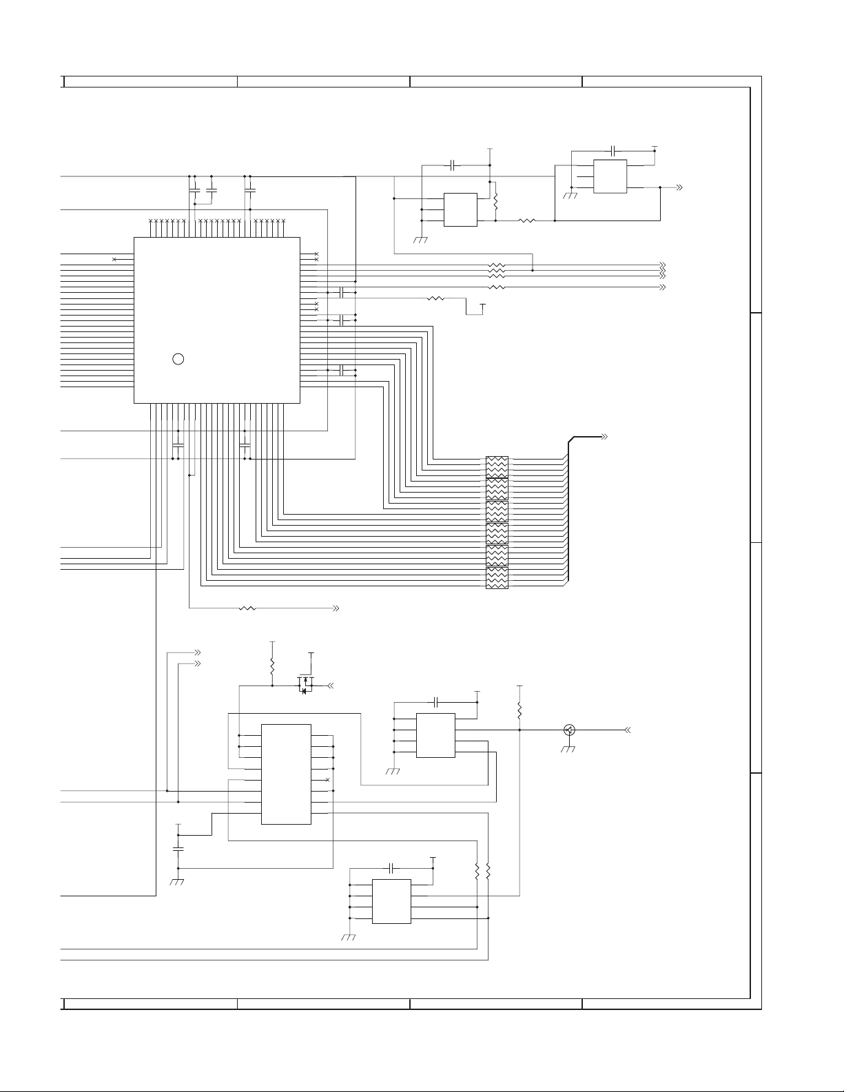
C224
C224
C204
C204
4.7u(3216)
4.7u(3216)
0.01u(B)
0.01u(B)
67
QO1669QO1770QO1871QO1972QO2073QO2174QO22
68
DGND
IC201
IC201
TFP503
TFP503
66
CAP
75
76
OGND
77
QO23
78
OVDD
79
AGND
80
RX2+
81
RX2-
82
AVDD
83
RX1+
84
RX1-
85
AVDD
86
RX0+
87
RX0-
88
AVDD
89
RXC+
90
RXC-
91
AVDD
92
DDC_SCL
93
DDC_SDA
94
DDC_SA
95
RCL
96
RDA
97
PVDD1
98
PGND
99
PVDD2
100
OCK_INV
DFO1/PD2ST3PIXS4DGND5DVDD6/STAG7SCDT8/PDO9QE010QE111QE212QE313QE414QE515QE616QE717OVDD18OGND19QE820QE921QE1022QE1123QE1224QE13
C216
C216
0.01u(B)
0.01u(B)
1234
2/9
C202
C202
0.1u
0.1u
5
VDD
4
OPORTA[23:0] 3,4
MAIN_+3.3V
DVI_HS 3,4
DVI_VS 3,4
DVI_DE 3,4
DVI_DCLK 3,4
CTL3 4
D
C
MAIN_+3.3V
C223NAC223
1
2
R247 10kR247 10k
NA
IC207NAIC207
ER
SUB
GND3VOUT
NA
R7
R6
R5
R4
R3
R2
R1
R0
G7
G6
G5
G4
G3
G2
G1
G0
B7
B6
B5
B4
B3
B2
B1
B0
VCC
5
4
R201 33R201 33
R202 33R202 33
R203 33R203 33
R204 33R204 33
MAIN_+3.3V
R235
NA
R236 NANA
OPORTA23
OPORTA22
OPORTA21
OPORTA20
OPORTA19
OPORTA18
OPORTA17
OPORTA16
OPORTA15
OPORTA14
OPORTA13
OPORTA12
OPORTA11
OPORTA10
OPORTA9
OPORTA8
OPORTA7
OPORTA6
OPORTA5
OPORTA4
OPORTA3
OPORTA2
OPORTA1
OPORTA0
C205
C205
0.01u(B)
0.01u(B)
56
60
57
58
OGND
OVDD
HSYNC
VSYNC
OGND
ODCK
OVDD
RSVD
CTL2
CTL1
DGND
DVDD
QE23
QE22
QE21
QE20
QE19
QE18
QE17
QE16
OVDD
OGND
QE15
QE14
25
QO251QO352QO453QO554QO655QO7
QO1
QO0
C217
C217
0.01u(B)
0.01u(B)
50
49
48
47
46
DE
45
44
43
42
41
40
39
38
37
36
35
34
33
32
31
30
29
28
27
26
C214
C214
0.01u(B)
0.01u(B)
C208 0.01u(B)C208 0.01u(B)
C210 0.01u(B)C210 0.01u(B)
QO859QO9
QO1061QO1162QO1263QO1364QO1465QO15
BR201
BR201
33*4
33*4
BR202
BR202
33*4
33*4
BR203
BR203
33*4
33*4
BR204
BR204
33*4
33*4
BR205
BR205
33*4
33*4
BR206
BR206
33*4
33*4
IC202
IC202
1
D
2
CLK
GND3/Q
SN74LVC1G80DBVR
SN74LVC1G80DBVR
MAIN_+3.3V
2
8
7
6
INH
5
3Y0
4
3
3Y1
2
2Y0
1
2Y1
1
Q207
Q207
2SK3018
2SK3018
3
RX_SCDT 4
DDC_SEL : L:AV H:PC
DDC_SEL 4
1
2
3
4
C220 0.1uC220 0.1u
IC205
IC205
A0
VCC
A1
A2
SDA
GND
BR24L02F-WE2
BR24L02F-WE2
PC
WP
SCL
AV
C218 0.1uC218 0.1u
IC204
IC204
1
A0
2
A1
3
A2
GND4SDA
BR24L02F-WE2
BR24L02F-WE2
AV_SCL
AV_SDA
PC_SDA
DDCD_+5V
8
7
6
5
B
R2330R233
0
DDCD_+5V
R220
R220
10k
10k
Q202
Q202
DTC115EUAT106
DTC115EUAT106
3 2
1
DDC_W 1,4
DDCD_+5V
8
VCC
7
WP
6
SCL
5
R2320R232
0
A
21
R218 33R218 33
DDCD_+5V
DDCD_+5V
C219
C219
0.1u
0.1u
DVI_SCL 4
DVI_SDA 4
IC203
IC203
SN74LV4053APWR
SN74LV4053APWR
9
10
11
12
13
14
15
16
PC_SCL
C
B
A
1Y0
1Y1
1-COM
2-COM
VCC
R219
R219
10k
10k
3
GND
GND
3-COM
SEL : H:PC L:AV
4
PN-525U CIRCUIT DIAGRAM & PARTS LAYOUT
7 – 4
Page 68

5678
OUTPUT
D
C
circuit of I/F1 PWB
2,4
OPORTA[23:0]
DVI_DCLK2,4
DVI_DE2,4
DVI_HS2,4
2,4
DVI_VS
DVI_PD4
OPORTA23
OPORTA22
OPORTA21
OPORTA20
OPORTA19
OPORTA18
OPORTA17
OPORTA16
OPORTA15
OPORTA14
OPORTA13
OPORTA12
OPORTA11
OPORTA10
OPORTA9
OPORTA8
OPORTA7
OPORTA6
OPORTA5
OPORTA4
OPORTA3
OPORTA2
OPORTA1
OPORTA0
R314NAR314
NA
L304
L304
MLF1608D47NM
MLF1608D47NM
BR307 33*4BR307 33*4
R7
R6
R5
R4
R3
R2
R1
R0
G7
G6
G5
G4
48
47
DGND
49
R358 NAR358 NA
R3150R315
0
R316NAR316
NA
NC
50
DATA11
51
DATA10
52
DATA9
53
DATA8
54
DATA7
55
DATA6
56
IDCK-
57
IDCK+
58
DATA5
59
DATA4
60
DATA3
61
DATA2
62
DATA1
63
DATA0
64
DGND
DVDD1DE2VREF3HSYNC4VSYNC5DK36RDA7RCL8EDGE/HTPLG9/PD10MSEN11DVDD12ISEL//RST13DSEL/SDA14BSEL/SCL15DGND
C307
C307
0.01u(B)
0.01u(B)
C308
C308
100p
100p
IC301
IC301
TFP513
TFP513
G3
G2
G1
G0
B7
B6
B5
B4
B3
B2
B1
B0
R3030R303
0
MAIN_+3.3V
R356 2.2kR356 2.2k
2,4
MSTR0_SDA
MSTR0_SCL2,4
MSTR2_SCL4
MSTR2_SDA4
DVI_TX_RST4
R357 2.2kR357 2.2k
R359 NAR359 NA
R313 0R313 0
C301
C301
0.01u(B)
0.01u(B)
35
33
DVDD
DATA2336DATA2237DATA2138DATA2039DATA1940DATA1841DATA1742DATA1643DATA1544DATA1445DATA1346DATA12
32
TGND
31
TX2+
RESERVED34RESERVED
30
TX2-
29
TVDD
28
TX1+
27
TX1-
26
TGND
25
TX0+
24
TX0-
23
TVDD
22
TXC+
21
TXC-
20
TGND
19
TFADJ
18
PVDD
17
PGND
16
10u(2012)
10u(2012)
C310
C310
C309
C309
0.01u(B)
0.01u(B)
R363
R363
4.7k
4.7k
B
R326NAR326
NA
R332
R332
220k
220k
Y_BNC1
CVBS1
Pb_BNC1
A.GND
A.GND A.GND A.GND
A
Pr_BNC1
VIDEO_+5VVIDEO_+5V VIDEO_+5V VIDEO_+5VVIDEO_+5V
R333
R333
R327NAR327
R328NAR328
NA
R334
R334
330k
330k
VIDEO_+5VVIDEO_+5V
T_P301T_P301
T_P303T_P303
R329NAR329
R335NAR335
NA
NA
330k
330k
NA
R331NAR331
R336
R336
A.GND A.GND
R330NAR330
R337
R337
NA
C312
C312
C313
C313
0.1u
0.1u
0.1u
330k
330k
0.1u
1
2
3
4
5
6
7
8
9
10
11
12
13
NA
330k
330k
C314
C314
C315
C315
0.1u
0.1u
0.1u
0.1u
IC302
IC302
GINA
GSG1
GINB
NC
BINA
GSB1
SYNCIN
BINB
MUXSEL
NC
DISABLE
GND3
BOUT
VCC3
GND2
GOUT14VCC2
GND29GND
30
A.GND
RINB
GSR1
RINA
VCC4
VFC
RFC
GND4
VCC1
ROUT
GND1
NC
C316
C316
10u(2012)
10u(2012)
28
27
26
25
24
23
22
21
20
19
18
17
16
15
SM5301CS-G
SM5301CS-G
A.GND
C321
33p
A.GND
8765
PN-525U CIRCUIT DIAGRAM & PARTS LAYOUT
7 – 5
Page 69

D313
D313
RB070M-30
RB070M-30
1234
3/9
MAIN_+5V
12
R364NAR364
NA
C302
C302
10u(2012)
10u(2012)
C305
C305
100p
100p
C311
C311
10u(2012)
10u(2012)
R305
R305
4.7k
4.7k
L301
L301
BLM18PG221SN1D
BLM18PG221SN1D
R302
R302
510(D)
510(D)
L302
L302
BLM18PG221SN1D
BLM18PG221SN1D
L303
L303
BLM18PG221SN1D
BLM18PG221SN1D
R306
R306
4.7k
4.7k
R307
R307
10k
10k
C303
C303
100p
100p
C304 100pC304 100p
R308NAR308
NA
MAIN_+3.3V
+
+
R309NAR309
NA
R310NAR310
NA
CE301
CE301
47u/25V
47u/25V
R311NAR311
NA
MAIN_+3.3V
D301NAD301
NA
R312
R312
2.2k
2.2k
R360 1kR360 1k
F301
F301
11CT 1A
11CT 1A
CN301
CN301
1
TX2-
2
TX2+
3
GND
4
TX4-
5
TX4+
6
DCLK
7
DDATA
8
A V
9
TX1-
10
TX1+
11
GND
12
TX3-
13
TX3+
14
VDD
15
GND
16
HPDETECT
17
TX0-
18
TX0+
19
GND
20
TX5-
21
TX5+
22
GND
23
TXC+
24
TXC-
D308NAD308
NA
MAIN_+5V
2 3
1
2 3
1
2 3
3
1
MAIN_+5V
1
2 3
D307NAD307
D306NAD306
NA
NA
R362
R362
10k
10k
2 3
2SK3018
2SK3018
1
2 3
1
D303NAD303
NA
MAIN_+3.3V
2
Q303
Q303
1
Q304
Q304
2SK3018
2SK3018
D304NAD304
NA
2 3
1
D305NAD305
NA
R361
R361
10k
10k
3
2
1
2 3
1
D302NAD302
NA
74320-4004
74320-4004
D
C
R347
R347
1.6k(D)
1.6k(D)
R318NAR318
NA
C322
C322
2.2u(3216)
2.2u(3216)
R353 10kR353 10k
4
R320NAR320
NA
1 2
R322
R319NAR319
NA
VIDEO_+5V
R322
R3210R321
100k
100k
0
D312
D312
HZU3.3B2
HZU3.3B2
VIDEO_+5V
R338NAR338
NA
R3390R339
0
A.GND
R342 47kR342 47k C320
3 2
Q301
Q301
1
DTC114EUAT106
DTC114EUAT106
R323NAR323
NA
R324NAR324
NA
R343 47kR343 47k
C323
C323
2.2u(3216)
2.2u(3216)
R352 NAR352 NA
BNC_SEL 4
A.GND
R351NAR351
R346NAR346
NA
R325NAR325
NA
VIDEO_+5V
R355
R355
10k
10k
R34520R345
20
CVBS_TH1
R348 20R348 20
R349 20R349 20
R350 20R350 20
NA
A.GND
3
2
Q302
Q302
1
DTC115EUAT106
DTC115EUAT106
C320
0.1u(B)
0.1u(B)
R354 NAR354 NA
C325
C325
0.1u(B)
0.1u(B)
C326
C326
0.1u(B)
0.1u(B)
BNC_SEL
H :AV
L: ANA
3
D_SEL 4
VFC_PWM 4
Pr_IN 4
C324
C324
0.1u(B)
0.1u(B)
Y_IN 4
Pb_IN 4
CVBS_O 4
2 3
1
2 3
1
MAIN_+5V
2 3
1
B
D309
D309
BAV99
BAV99
A.GND
R34020R340
20
R34120R341
20
R34420R344
20
D310
D310
BAV99
BAV99
C317
C317
0.1u(B)
0.1u(B)
C318
C318
0.1u(B)
0.1u(B)
C319
C319
0.1u(B)
0.1u(B)
D311
D311
BAV99
BAV99
A_RET 4
B_RET 4
C_RET 4
A
21
PN-525U CIRCUIT DIAGRAM & PARTS LAYOUT
7 – 6
Page 70

5678
CORTEZ
D
C
circuit of I/F1 PWB
MAIN_+2.5V
MAIN_+3.3V
L401
L401
BLM18PG121SN1D
BLM18PG121SN1D
CE401
CE401
47u/6.3V
47u/6.3V
L402
L402
BLM18PG121SN1D
BLM18PG121SN1D
CE403
CE403
47u/6.3V
47u/6.3V
C443
C443
0.1u(1005)
0.1u(1005)
C457
C457
0.1u
0.1u
C401
C401
C403
C403
0.1u(1005)
0.1u(1005)
0.01u(1005)
0.01u(1005)
+
+
+
+
C402
C402
CE402
CE402
0.01u(1005)
0.01u(1005)
47u/6.3V
47u/6.3V
C420
C420
C422
C422
0.1u(1005)
0.1u(1005)
0.1u(1005)
0.1u(1005)
+
+
C421
C421
C419
C419
0.1u(1005)
0.1u(1005)
0.1u(1005)
0.1u(1005)
C430
C430
0.1u
0.1u
C431
C431
0.01u(B)
0.01u(B)
C438
C438
0.1u
0.1u
C439
C439
0.1u
0.1u
C445
C445
0.1u(1005)
0.1u(1005)
C444
C444
C446
C446
0.1u(1005)
0.1u(1005)
0.1u(1005)
0.1u(1005)
PLL_+1.8V
C459
C459
0.1u
0.1u
C460
C460
0.1u
0.1u
C458
C458
0.1u
0.1u
C432
C432
0.01u(B)
0.01u(B)
C447
C447
0.1u(1005)
0.1u(1005)
C404
C404
0.01u(1005)
0.01u(1005)
C423
C423
0.1u(1005)
0.1u(1005)
PLL_+3.3V
+
+
CE404
CE404
47u/6.3V
47u/6.3V
ADC1_+3.3V
C440
C440
0.1u
0.1u
C448
C448
0.1u(1005)
0.1u(1005)
C405
C405
0.01u(1005)
0.01u(1005)
C424
C424
0.1u(1005)
0.1u(1005)
+
+
CE405
CE405
NA
NA
C441
C441
0.1u
0.1u
C449
C449
0.1u(1005)
0.1u(1005)
C407
C407
0.01u(1005)
0.01u(1005)
C406
C406
0.01u(1005)
0.01u(1005)
C426
C426
0.1u(1005)
0.1u(1005)
C425
C425
0.1u(1005)
0.1u(1005)
R460 0R460 0
LVDS_+3.3V
CE407
CE407
+
+
47u/6.3V
47u/6.3V
C451
C451
0.1u(1005)
0.1u(1005)
C450
C450
0.1u(1005)
0.1u(1005)
C461
C461
0.1u
0.1u
C408
C408
0.01u(1005)
0.01u(1005)
C436
C436
0.1u(1005)
0.1u(1005)
C452
C452
0.1u(1005)
0.1u(1005)
C409
C409
0.01u(1005)
0.01u(1005)
C427
C427
0.1u(1005)
0.1u(1005)
C433
C433
0.01u(B)
0.01u(B)
C453
C453
0.1u(1005)
0.1u(1005)
ADC_+1.8V
C462
C462
0.1u
0.1u
C410
C410
0.01u(1005)
0.01u(1005)
C437
C437
0.1u(1005)
0.1u(1005)
C454
C454
0.1u(1005)
0.1u(1005)
C411
C411
0.01u(1005)
0.01u(1005)
C428
C428
0.1u(1005)
0.1u(1005)
C412
C412
0.01u(1005)
0.01u(1005)
I/O_+3.3V
ADC2_+3.3V
C434
C434
0.01u(B)
0.01u(B)
LBADC_+3.3V
C442
C442
0.1u
0.1u
C455
C455
0.1u(1005)
0.1u(1005)
C456
C456
0.1u(1005)
0.1u(1005)
C413
C413
0.01u(1005)
0.01u(1005)
C429
C429
0.1u(1005)
0.1u(1005)
CE408
CE408
47u/6.3V
47u/6.3V
C414
C414
0.01u(1005)
0.01u(1005)
C435
C435
0.1u
0.1u
CORE_+1.8V
+
+
C417
C417
+
+
0.01u(1005)
0.01u(1005)
CE409
CE409
47u/6.3V
47u/6.3V
C463
C463
27p
27p
GMAIN_+2.5V
T_P401T_P401
T_P402T_P402
T_P408T_P408
T_P403T_P403
T_P404T_P404
T_P405T_P405
LVDS_PLL_+3.3V
CE406
CE406
+
+
22u/16V
22u/16V
PLL_+3.3V
C418
C418
0.01u(1005)
0.01u(1005)
Y401
Y401
19.6608MHz
19.6608MHz
R401
R401
10k
10k
PLL_+3.3V
GREEN_DSUB1
G_BNC1
Y_IN3
A_RET3
BLUE_DSUB1
B_BNC1
Pb_IN3
B_RET3
RED_DSUB1
R_BNC1
Pr_IN3
C_RET3
CVBS_O3
SV_RET1
AHSYNC1
R404
R404
R403
R403
R406
R406
10k
10k
10k
10k
10k
10k
R454NAR454
NA
C464
C464
18p
18p
A.GND
R405
R405
R402
R402
10k
10k
10k
10k
A.GND
DVI_DCLK2,3
AVSYNC1
OPORTA[23:0]2,3
DVI_VS2,3
DVI_HS2,3
DVI_DE2,3
2
R408 0R408 0
R409 0R409 0
R410 0R410 0
FAN2
6
REMO18
REMO28
REMO38
L403
L403
MLF1608D47NM
MLF1608D47NM
DVI_TX_RST3
PR1_WP
PR2_WP
BL_CNT
6
AUD_POW
9
PC_BNC_SEL
1
R416 0R416 0
DVI_PD3
R417 0R417 0
DVI_IN_PD2
R418 0R418 0
CTL3
R419 0R419 0
RX_SCDT2
OPORTA0
OPORTA1
OPORTA2
OPORTA3
OPORTA4
OPORTA5
OPORTA6
OPORTA7
OPORTA8
OPORTA9
OPORTA10
OPORTA11
OPORTA12
OPORTA13
OPORTA14
OPORTA15
OPORTA16
OPORTA17
OPORTA18
OPORTA19
OPORTA20
OPORTA21
OPORTA22
OPORTA23
PPWR9
ANA_SEL
6
T_P412T_P412
T_P413T_P413
T_P414T_P414
T_P415T_P415
T_P416T_P416
T_P417T_P417
T_P418T_P418
T_P419T_P419
T_P420T_P420
T_P421T_P421
T_P422T_P422
T_P423T_P423
T_P424T_P424
T_P425T_P425
T_P427T_P427
T_P429T_P429
T_P432T_P432
R455 33R455 33
T_P409T_P409
T_P406T_P406
T_P407T_P407
T_P410T_P410
6
PWM0
VFC_PWM3
RESET_9539
IR6
INT9539_01
RESET_9539
6
6
R453 33R453 33
SELLVDS6
R/L6
U/D6
FRAME6
O/Sset6
TEMP3
TEMP26
TEMP1
R423 33R423 33
R424 33R424 33
R427 NAR427 NA
R428 NAR428 NA
R429 33R429 33
R430 33R430 33
R431 33R431 33
R432 33R432 33
RxD_OUT7
TxD_IN7
C471NAC471
7
TxD_OUT
NA
RxD_IN7
6
MSTR1_SDA
MSTR1_SCL
6
MSTR2_SDA3
3
MSTR2_SCL
VGA0_SDA1
1
VGA0_SCL
2
DVI_SDA
DVI_SCL2
TILT17
7
TILT2
AMP_ER6
HPD2
1,3
BNC_SEL
FAN16
12V_SEN8
UART_INTR1
7
INT9539_01
BR440
BR440
33*4
33*4
BR442
BR442
33*4
33*4
5,6,7
Q403 DTC114EUAT106Q403 DTC114EUAT106
3 2
R462
R462
2.2
2.2
14
Y402
Y402
32.768kHz
32.768kHz
12
D401
D401
1SS355
1SS355
CE410
CE410
+
+
+
+
1.0F
1.0F
MAIN_+3.3V
R4221kR422
1k
C465NAC465
NA
/RESET
1
R461 470kR461 470k
C477
C477
1u(B)
1u(B)
1
2
3
4
C474 0.1u(1005)C474 0.1u(1005)
IC403
IC403
X1
X2
Vbac
/RST
GND5SDA
DS1374U-33+
DS1374U-33+
PR2_WPPR1_WP
VCC
SQW
/INT
SCL
C475
C475
0.1u(1005)
0.1u(1005)
1
2
IC405 TC7S86FIC405 TC7S86F
9
6
MAIN_+3.3V
10
9
8
7
6
IN B
IN A
GND3OUT
TH69
TH5
TH49
TH39
TH29
TH1
C466NAC466
NA
A.GND
R437
R437
R438
R438
10k
10k
10k
10k
MAIN_+3.3V
5
VCC
4
C470NAC470
C467NAC467
C468NAC468
C469NAC469
NA
NA
NA
NA
BR430
BR430
33*4
33*4
BR444
BR444
33*4
33*4
2
3
Q406
Q406
1
DTC114EUAT106
DTC114EUAT106
MAIN_+5V
B
I2C_5V_SDA1,6
I2C_5V_SCL1,6
MSTR0_SDA2,3
MSTR0_SCL2,3
1
2
3
BR24L32FV-WE2
BR24L32FV-WE2
R420
R420
10k
10k
A0
A1
A2
GND4SDA
R421
R421
10k
10k
C472
C472
0.1u(1005)
0.1u(1005)
IC404
IC404
VCC
WP
SCL
MAIN_+3.3V
321
3
MAIN_+3.3V
8
7
6
5
Q401
Q401
2SK3018
2SK3018
2
Q402
Q402
2SK3018
2SK3018
1
R434
R434
10k
10k
3 2
1
Q404
Q404
DTC114EUAT106
DTC114EUAT106
R425
R425
10k
10k
1
A0
2
A1
3
A2
4
GND
BR24L32FV-WE2
BR24L32FV-WE2
MAIN_+3.3V
C473
C473
0.1u(1005)
0.1u(1005)
IC402
IC402
VCC
WP
SCL
SDA
R426
R426
10k
10k
8
7
6
5
MAIN_+3.3V
R436
R436
10k
10k
CE411
CE411
1.0F
1.0F
A
8765
PN-525U CIRCUIT DIAGRAM & PARTS LAYOUT
7 – 7
Page 71

CORE_+1.8V
IC401
IC401
K10
K11
K16
K17
L11
AB1
A1P
AF1
A2P
CORE_1.8
CORE_1.8
CORE_1.8
AF4
A3P
AF7
AN2
AD1
AN
AC2
B1P
AE2
B2P
AE5
B3P
AE8
BN2
AF3
BN
AC1
C1P
AF2
C2P
AF5
C3P
AF8
CN2
AF6
CN
AB2
SV1P
AE1
SV2P
AE4
SV3P
AE7
SV4P
AF9
SVN
AC7
VOUT2
AF12
AIP_RAW_HS_CS
AE12
AIP_RAW_VS
AD13
EXT_OSD_VS/GPIO_8(0)
AC13
EXT_OSD_HS/GPIO_8(1)
AF13
EX_OSD_CLK/GPIO_8(2)
P3
ADATA0/GPIO_0(0)
P2
ADATA1/GPIO_0(1)
P1
ADATA2/GPIO_0(2)
R4
ADATA3/GPIO_0(3)
R3
ADATA4/GPIO_0(4)
R2
ADATA5/GPIO_0(5)
R1
ADATA6/GPIO_0(6)
T4
ADATA7/GPIO_0(7)
T3
ADATA8/GPIO_1(0)
T2
ADATA9/GPIO_1(1)
T1
ADATA10/GPIO_1(2)
U4
ADATA11/GPIO_1(3)
U3
ADATA12/GPIO_1(4)
U2
ADATA13/GPIO_1(5)
U1
ADATA14/GPIO_1(6)
V4
ADATA15/GPIO_1(7)
V3
ADATA16/GPIO_2(0)
V2
ADATA17/GPIO_2(1)
V1
ADATA18/GPIO_2(2)
W4
ADATA19/GPIO_2(3)
W3
ADATA20/GPIO_2(4)
W2
ADATA21/GPIO_2(5)
W1
ADATA22/GPIO_2(6)
Y4
ADATA23/GPIO_2(7)
Y1
AVS/GPIO_16
Y2
AHS/GPIO_17
Y3
AHREF_DE/GPIO_18
N3
DIP_AODD/GPIO_26
N2
DIP_RAW_HS_CS
M1
DIP_CLEAN_HS_OUT/GPIO_22
M2
DIP_EXP_CLAMP/GPIO_23
M3
DIP_EXT_COAST/GPIO_24
N1
IPCLK0
P4
IPCLK1
M4
IPCLK2/GPIO_14
L1
IPCLK3/GPIO_15
B1
BDATA0/GPIO_3(0)
C3
BDATA1/GPIO_3(1)
C2
BDATA2/GPIO_3(2)
C1
BDATA3/GPIO_3(3)
D3
BDATA4/GPIO_3(4)
D2
BDATA5/GPIO_3(5)
D1
BDATA6/GPIO_3(6)
E3
BDATA7/GPIO_3(7)
E2
BDATA8/GPIO_4(0)
E1
BDATA9/GPIO_4(1)
F3
BDATA10/GPIO_4(2)
F2
BDATA11/GPIO_4(3)
F1
BDATA12/GPIO_4(4)
G3
BDATA13/GPIO_4(5)
G2
BDATA14/GPIO_4(6)
G1
BDATA15/GPIO_4(7)
H3
BDATA16/GPIO_5(0)
H2
BDATA17/GPIO_5(1)
H1
BDATA18/GPIO_5(2)
J3
BDATA19/GPIO_5(3)
J2
BDATA20/GPIO_5(4)
J1
BDATA21/GPIO_5(5)
K3
BDATA22/GPIO_5(6)
K2
BDATA23/GPIO_5(7)
L2
BVS/GPIO_19
L3
BHS/GPIO_20
K1
BHREF_DE/GPIO_21
N4
DIP_BODD/GPIO_27
B26
XTAL
C26
TCLK
V24
PWM0/GPIO_29
U23
PWM1/GPIO_30
U24
PWM2/GPIO_31
AB24
IR0/GPIO_28
AE11
LBADC_IN6
AF11
LBADC_IN5
AC10
LBADC_IN4
AD10
LBADC_IN3
AE10
LBADC_IN2
AF10
LBADC_IN1
AD11
LBADC_RETURN
W26
OCM_UDO_0/GPIO_7
W25
OCM_UDI_0/GPIO_8
B2
OCM_UDO_1/GPIO_10
B3
OCM_UDI_1/GPIO_11
AD9
/RESETn
AA23
MSTR0_SDA/GPIO_32
AA24
MSTR0_SCL/GPIO_33
A2
MSTR1_SDA/GPIO_34
A3
MSTR1_SCL/GPIO_35
AB25
MSTR2_SDA/GPIO_36
AB26
MSTR2_SCL/GPIO_37
AA25
VGA0_SDAGPIO_38
AA26
VGA0_SCL/GPIO_39
Y25
VGA1_SDA/GPIO_40
Y26
VGA1_SCL/GPIO_41
AD14
AVS_OUT_DATA/GPIO_7(0)
AE13
AVS_OUT_SCL/JTAG_TDO/GPIO_7(1)
AE14
AVS_OUT_WORD_SEL/JTAG_OCM_RESET/GPIO_7(2)
AC12
AVS_IN_DATA/JTAG_OCM_TDI/GPIO_7(3)
AF14
AVS_IN_SCL/JTAG_OCM_CLK/GPIO_7(4)
AD12
AVS_IN_WORD_SEL/JTAG_OCM_MODE/GPIO_7(5)
Y24
OCM_INT2/GPIO_5
W23
OCM_INT1/GPIO_6
W24
OCM_TIMER1/PWW3/GPIO_9
V26
SLAVE_SCL/GPIO_12
V25
SLAVE_SDA/GPIO_25
D25
N/C
A1
N/C
AA1
N/C
CORE_1.8
D_GND
D_GND
D_GND
D_GND
D_GND
D_GND
D_GND
L10
T10
P10
R10
N11
N10
M11
M10
1234
4/9
FSVREF
C415
C415
C416
I/O_+3.3V
L16
T11
CORE_1.8
CORE_1.8
D_GND
D_GND
P11
R11
F4
T16
T17
U10
U11
U16
U17
IO_3.3G4IO_3.3H4IO_3.3J4IO_3.3
IO_3.3E4IO_3.3
CORE_1.8
CORE_1.8
CORE_1.8
CORE_1.8
CORE_1.8
CORE_1.8
CORE_1.8
D_GND
D_GND
D_GND
D_GND
D_GND
D_GND
D_GND
D_GND
D_GND
D_GND
D_GND
D_GND
D_GND
L13
L12
T12
P13
K13
P12
K12
N13
N12
R12
U12
M13
M12
BR434NABR434
NA
LBADC_+3.3V LVDS_PLL_+3.3V
K4
AC14
AC16
AC18
AB23
Y23
V23
T23
P23
M23
AC22
IO_3.3L4IO_3.3
IO_3.3
IO_3.3
IO_3.3
IO_3.3
IO_3.3
IO_3.3
IO_3.3
D_GND
D_GND
D_GND
D_GND
D_GND
D_GND
D_GND
D_GND
D_GND
D_GND
D_GND
D_GND
L14
T14
T13
K15
P14
K14
R13
R14
N14
U13
U14
M14
MAIN_+3.3V MAIN_+3.3V
R444NAR444
R449 33R449 33
R451 10kR451 10k
R450 NAR450 NA
NA
R443
R443
10k
10k
BR435NABR435
NA
D10
AC9
IO_3.3
IO_3.3
DDR_2.5D4DDR_2.5D6DDR_2.5D8DDR_2.5
DDR_2.5D7DDR_2.5
LBACD-3.3
D_GND
D_GND
D_GND
D_GND
D_GND
D_GND
D_GND
D_GND
D_GND
D_GND
D_GND
L15
T15
P16
P15
R16
U15
R15
N16
N15
M16
M15
R448
R448
10k
10k
IC406
IC406
1
/INT
VCC
2
SDA
A1
3
A2
SCL
4
P00
A0
5
P01
P17
6
P02
P16
7
P03
P15
8
P04
P14
9
P05
P13
10
P06
P12
11
P07
P11
12
GND
P10
PCF8575
PCF8575
C416
0.1u
0.1u
0.1u
0.1u
LVDS_+3.3V
D11
D14
D15
D17
D20
D22
D23
D12
D13
D18
H24
C19
C9
FSVREF
DDR_2.5
DDR_2.5
DDR_2.5
DDR_2.5
D_GND
D_GND
P17
R17
FLI8638
FLI8638
C476 0.1u(1005)C476 0.1u(1005)
DDR_2.5
DDR_2.5
DDR_2.5
D_GND_ADC
D_GND_ADC
D_GND_ADC
AA3
AA4
AA2
R445NAR445
NA
R452 10kR452 10k
FSVREF
LVDS_PLL_3.3
LVDS_GND
LVDS_GND
LVDS_GND
LVDS_GND
LVDS_GND
J25
E25
H25
M25
M24
R446
R446
10k
10k
DDR_2.5
DDR_2.5
D_GND
D_GND
D_GND
D_GND
L17
N17
M17
24
23
22
21
20
19
18
17
16
15
14
13
PLL_+1.8V
ADC_+1.8V
PLL_+3.3V
E26
H26
LVDS_3.3
LVDS_PLL_GND
H23
C25
J26
M26
AC5
AC4
AB4
A14
ADC_1.8
ADC_1.8
ADC_1.8
RPLL_1.8
LVDS_3.3
LVDS_3.3
LVDS_3.3
VDD18_DLL
AGND_ADC
AGND_ADC
AGND_ADC
AGND_ADC
AGND_ADC
AGND_ADC
AGND_ADC
AGND_ADC
AE3
AE6
AB3
AE9
AC6
AC8
AD8
AC3
AD2
BR436NABR436
NA
BR437NABR437
NA
ADC1_+3.3VGMAIN_+2.5V
AD3
AD4
AD5
D26
RPLL_33
ADC1_3.3
ADC1_3.3
ADC1_3.3
CLKN_LV_E/PD5(EBULU5)
CLKP_LVE/PD4(EBULU4)
CH2N_LV_E/PD7(EBLU7)
CH2P_LV_E/PD6(EBLU6)
CH1N_LV_E/PD9(EGRN1)
CH1P_LV_E/PD8(EGRN0)
CH0N_LV_E/PD11(EGRN3)
CH0P_LV_E/PD10(EGRN2)
CH4N_LV_O/PD13(EGRN5)
CH4P_LV_O/PD12(EGRN4)
CH3N_LV_O/PD15(EGRN7)
CH3P_LV_O/PD14(EGRN6)
CLKN_LV_O/PD17(ERED1)
CLKP_LV_O/PD16(ERED0)
CH2N_LV_O/PD19(ERED3)
CH2P_LV_O/PD18(ERED2)
CH1_LV_O/PD21(ERED5)
CH1P_LV_O/PD20(ERED4)
CH0N_LV_O/PD23(ERED7)
CH0P_LV_O/PD22(ERED6)
CH4P_LV_E/PD0(EBLU0)
CH4N_LV_E/PD1(EBLU1)
CH3P_LV_E/PD2(EBLU2)
CH3N_LV_E/PD3(EBLU3)
OCMDATA15/GPIO_6(7)
OCMDATA14/GPIO_6(6)
OCMDATA13/GPIO_6(5)
OCMDATA12/GPIO_6(4)
OCMDATA11/GPIO_6(3)
OCMDATA10/GPIO_6(2)
/OCM_CS0n/XROM_STATUS/GPIO_2
VSSA18_DLL
RPLL_AGND
RPLL_AGND
LBADC_GND
AGND_ADC
B14
A25
A26
AC11
MAIN_+3.3V
BR438NABR438
NA
ADC2_+3.3V
AD6
AD7
ADC2_3.3
ADC2_3.3
FSDATA0
FSDATA1
FSDATA2
FSDATA3
FSDATA4
FSDATA5
FSDATA6
FSDATA7
FSDATA8
FSDATA9
FSDATA10
FSDATA11
FSDATA12
FSDATA13
FSDATA14
FSDATA15
FSDATA16
FSDATA17
FSDATA18
FSDATA19
FSDATA20
FSDATA21
FSDATA22
FSDATA23
FSDATA24
FSDATA25
FSDATA26
FSDATA27
FSDATA28
FSDATA29
FSDATA30
FSDATA31
FSADDR0
FSADDR1
FSADDR2
FSADDR3
FSADDR4
FSADDR5
FSADDR6
FSADDR7
FSADDR8
FSADDR9
FSADDR10
FSADDR11
FSADDR12
FSCLKp
FSCLKn
FSDQS0
FSDQS1
FSDQS2
FSDQS3
FSDQM0
FSDQM1
FSDQM2
FSDQM3
FSBKSEL0
FSBKSEL1
DCLK/GPIO_9(4)
DHS/GPIO_9(5)
DVS/GPIO_9(6)
DEN/GPIO_9(7)
OCMADDR21/GPIO_1
OCMADDR20/GPIO_0
OCMADDR19/GPIO_13
OCMADDR18
OCMADDR17
OCMADDR16
OCMADDR15
OCMADDR14
OCMADDR13
OCMADDR12
OCMADDR11
OCMADDR10
OCMADDR9
OCMADDR8
OCMADDR7
OCMADDR6
OCMADDR5
OCMADDR4
OCMADDR3
OCMADDR2
OCMADDR1
OCMADDR0
OCMDATA9/GPIO_6(1)
OCMDATA8/GPIO_6(0)
OCMDATA7
OCMDATA6
OCMDATA5
OCMDATA4
OCMDATA3
OCMDATA2
OCMDATA1
OCMDATA0
/OCM_REn
/OCM_WEn
/ROM_CSn
/OCM_CS1n/GPIO_3
/OCM_CS2n/GPIO_4
JTAG_BS_EN
GPIO_42
GPIO_43
GPIO_44
GPIO_45
GPIO_46
GPIO_47
RPLL_DGND
FSVREFVSS
FSVREFVSS
D9
B25
D19
BR439NABR439
NA
FSCS0
FSCS1
FSWE
FSCAS
FSRAS
FSCKE
PPWR
PBIAS
MAIN_+3.3V
R456NAR456
NA
D
C
B
A
BR401
BR401
33*4
33*4
BR402
BR402
33*4
33*4
BR403
BR403
33*4
33*4
BR404
BR404
33*4
33*4
BR405
BR405
33*4
33*4
BR406
BR406
33*4
33*4
BR407
BR407
33*4
33*4
BR408
BR408
33*4
33*4
BR409
BR409
33*4
33*4
BR410
BR410
33*4
33*4
BR411
BR411
33*4
33*4
R407 33R407 33
BR412
BR412
33*4
33*4
BR413
BR413
33*4
33*4
BR421
BR421
33*4
33*4
BR422
BR422
33*4
33*4
BR423
BR423
33*4
33*4
BR424
BR424
33*4
33*4
BR425
BR425
33*4
33*4
BR426
BR426
33*4
33*4
BR427
BR427
33*4
33*4
BR428
BR428
33*4
33*4
BR429
BR429
33*4
33*4
FSDATA[31:0] 5
FSADDR[12:0] 5
FSCLK+ 5
FSCLK- 5
/FSCS0 5
FSDQS[3:0] 5
FSDQM[3:0] 5
/FSWE 5
/FSCAS 5
/FSRAS 5
FSCKE 5
FSBKSEL0 5
FSBKSEL1 5
TXB3- 6
TXB3+ 6
TXBC- 6
TXBC+ 6
TXB2- 6
TXB2+ 6
TXB1- 6
TXB1+ 6
TXB0- 6
TXB0+ 6
TXA3- 6
TXA3+ 6
TXAC- 6
TXAC+ 6
TXA2- 6
TXA2+ 6
TXA1- 6
TXA1+ 6
TXA0- 6
TXA0+ 6
OCMADDR[21:0] 5,7
OCMDATA[15:0] 5,7
/OCM_RE 5,7
/OCM_WE 5,7
/ROM_CSN 5
/OCM_CS0 5
/OCM_CS1 5
/OCM_CS2 7
BR441
BR441
33*4
33*4
BR443
BR443
33*4
33*4
BR414
BR414
33*4
33*4
OCMADDR21
OCMADDR20
OCMADDR19
OCMADDR18
OCMADDR17
OCMADDR16
OCMADDR15
OCMADDR14
OCMADDR13
OCMADDR12
OCMADDR11
OCMADDR10
OCMADDR9
OCMADDR8
OCMADDR7
OCMADDR6
OCMADDR5
OCMADDR4
OCMADDR3
OCMADDR2
OCMADDR1
OCMADDR0
OCMDATA15
OCMDATA14
OCMDATA13
OCMDATA12
OCMDATA11
OCMDATA10
OCMDATA9
OCMDATA8
OCMDATA7
OCMDATA6
OCMDATA5
OCMDATA4
OCMDATA3
OCMDATA2
OCMDATA1
OCMDATA0
BR431
BR431
33*4
33*4
MAIN_+3.3V
FSDATA0
FSDATA1
FSDATA2
FSDATA3
FSDATA4
FSDATA5
FSDATA6
FSDATA7
FSDATA8
FSDATA9
FSDATA10
FSDATA11
FSDATA12
FSDATA13
FSDATA14
FSDATA15
FSDATA16
FSDATA17
FSDATA18
FSDATA19
FSDATA20
FSDATA21
FSDATA22
FSDATA23
FSDATA24
FSDATA25
FSDATA26
FSDATA27
FSDATA28
FSDATA29
FSDATA30
FSDATA31
FSADDR0
FSADDR1
FSADDR2
FSADDR3
FSADDR4
FSADDR5
FSADDR6
FSADDR7
FSADDR8
FSADDR9
FSADDR10
FSADDR11
FSADDR12
T_P411T_P411
FSDQS0
FSDQS1
FSDQS2
FSDQS3
FSDQM0
FSDQM1
FSDQM2
FSDQM3
T_P434T_P434
UART_MF2 7
UART_TXRDY1 7
UART_MF1 7
UART_TXRDY2 7
UPDATE 7
B4
A4
B5
A5
B7
A7
B8
A8
B9
A9
B10
A10
B12
A12
B13
A13
B15
A15
B16
A16
B18
A18
B19
A19
B20
A20
B21
A21
B23
A23
B24
A24
C18
C17
C16
C15
C13
C10
C8
C7
C6
C12
D16
C14
C11
D5
C5
D21
C22
B6
B11
A17
A22
A6
A11
B17
B22
C23
D24
C24
C4
C21
C20
L24
L23
L26
L25
K24
K23
K26
K25
J24
J23
G24
G23
G26
G25
F24
F23
F26
F25
E24
E23
N23
N24
N25
N26
P24
P25
R26
P26
AF15
AE15
AD15
AC15
AF16
AE16
AD16
AF17
AE17
AD17
AC17
AF18
AE18
AD18
AF19
AE19
AD19
AC19
AF20
AE20
AD20
AF21
AE21
AD21
AC21
AF22
AE22
AD22
AF23
AE23
AD23
AC23
AF24
AF25
AF26
AE24
AE25
AE26
AC25
AC26
AD24
AD25
AD26
AC24
AC20
T24
T25
T26
R23
R24
R25
U25
U26
R457NAR457
NA
R411 33R411 33
R412 33R412 33
TXB3TXB3+
TXBCTXBC+
TXB2TXB2+
TXB1TXB1+
TXB0TXB0+
TXA3TXA3+
TXACTXAC+
TXA2TXA2+
TXA1TXA1+
TXA0TXA0+
T_P426T_P426
T_P428T_P428
T_P430T_P430
KEY[1:0] 6
T_P431T_P431
KEY0
KEY1
LED1 6
LED2 6
R414 33R414 33
R415 33R415 33
R433 33R433 33
R435 33R435 33
R439 10kR439 10k
R441 33R441 33
LCD_ON 6
BL_EN 6
DDC_SEL : L : PC
DDC_W : L : PROTECT
RESET3440 : L : RESET
FAN_ON : L : OFF
FAN_SPDH : L : LOW SPEED
D_SEL : L : YPBPR H : COMPOSITE
AMP_MUTE : L
/ROM_WP : H : WRITE
MSTR0_SDA
MSTR0_SCL
DDC_SEL 2
DDC_W 1,2
RESET3440 6
FAN_ON 6
FAN_SPDH 6
D_SEL 3
AMP_MUTE 6
/ROM_WP 5
4
3
21
PN-525U CIRCUIT DIAGRAM & PARTS LAYOUT
7 – 8
Page 72

12345678
12345678
12345678
12345678
FSDATA[31:0]4
FSADDR[12:0]4
D
D
D
D
FSDQS[3:0]4
FSDQM[3:0]4
GMAIN_+2.5V
PN-525U CIRCUIT DIAGRAM & PARTS LAYOUT
C
C
C
C
7 – 9
OCMADDR[21:0]4,7
B
B
B
B
C504
C504
0.01u(1005)
0.01u(1005)
C505
C505
0.01u(1005)
0.01u(1005)
C506
C506
0.01u(1005)
0.01u(1005)
C507
C507
0.01u(1005)
0.01u(1005)
OCMADDR[21:0]
C508
C508
0.01u(1005)
0.01u(1005)
C509
C509
0.01u(1005)
0.01u(1005)
C510
C510
0.01u(1005)
0.01u(1005)
OCMADDR1
OCMDATA0
OCMDATA1
OCMDATA2
OCMDATA3
OCMDATA12
OCMDATA13
OCMDATA14
OCMDATA15
OCMADDR0
OCMADDR15
OCMADDR13
OCMADDR11
OCMADDR9
OCMADDR21
OCMADDR19
OCMADDR8
OCMADDR6
OCMADDR4
OCMADDR2
C511
C511
0.01u(1005)
0.01u(1005)
C514
C514
C512
C512
0.01u(1005)
0.01u(1005)
0.01u(1005)
0.01u(1005)
C515
C515
C513
C513
0.01u(1005)
0.01u(1005)
0.01u(1005)
0.01u(1005)
ROM_+3.3V
/OCM_CS0 /OCM_CS1
NA
C516
C516
0.01u(1005)
0.01u(1005)
CN501NACN501
1 2
3 4
5 6
7 8
9 10
11 12
13 14
15 16
18
17
19 20
21 22
23 24
25 26
28
27
29 30
31 32
33 34
36
35
37 38
39 40
41 42
43 44
45 46
47 48
49 50
C518
C518
C517
C517
0.01u(1005)
0.01u(1005)
FSDQS0
FSDQS1
FSDQS2
FSDQS3
FSDQM0
FSDQM1
FSDQM2
FSDQM3
0.01u(1005)
0.01u(1005)
C519
C519
0.01u(1005)
0.01u(1005)
/OCM_WE
/ROM_CS
/OCM_RE
OCMDATA8
OCMDATA9
OCMDATA10
OCMDATA11
OCMDATA4
OCMDATA5
OCMDATA6
OCMDATA7
OCMADDR17
OCMADDR16
OCMADDR14
OCMADDR12
OCMADDR10
OCMADDR20
OCMADDR18
OCMADDR7
OCMADDR5
OCMADDR3
FSADDR0
FSADDR1
FSADDR2
FSADDR3
FSADDR4
FSADDR5
FSADDR6
FSADDR7
FSADDR8
FSADDR9
FSADDR10
FSADDR11
FSADDR12
FSCLKFSCLK+
FSCKE FSCKE
/FSCS0
/FSRAS
/FSCAS
/FSWE
FSBKSEL1
FSBKSEL0
MT46V16M16P-5B
MT46V16M16P-5B
IC501
IC501
29
30
31
32
35
36
37
38
39
40
28
41
42
46
45
44
24
23
22
21
27
26
GMAIN_+2.5V
A0
VDDQ3VDDQ9VDDQ15VDDQ55VDDQ
A1
A2
A3
A4
A5
A6
A7
A8
A9
A10/AP
A11
A12
CLK
CLK
CKE
CS
RAS
CAS
WE
BA1
BA0
VSSQ6VSSQ12VSSQ58VSSQ64VSS34VSS48VSS
52
/ROM_WP
C503
C503
0.1u(1005)
0.1u(1005)
61
VDD1VDD18VDD
VSSQ
OCMADDR21
OCMADDR20
OCMADDR19
OCMADDR18
OCMADDR17
OCMADDR16
OCMADDR15
OCMADDR14
OCMADDR13
OCMADDR12
OCMADDR11
OCMADDR10
OCMADDR9
OCMADDR8
OCMADDR7
OCMADDR6
OCMADDR5
OCMADDR4
OCMADDR3
OCMADDR2
OCMADDR1
FSVREF
33
49
2
DQ0
VREF
4
DQ1
5
DQ2
7
DQ3
8
DQ4
10
DQ5
11
DQ6
13
DQ7
16
LDQS
20
LDM
54
DQ8
56
DQ9
57
DQ10
59
DQ11
60
DQ12
62
DQ13
63
DQ14
65
DQ15
51
UDQS
47
UDM
53
NC
50
NC
43
NC
25
NC
19
NC
17
NC
14
NC
66
MAIN_+3.3V
L501BLM18PG121SN1DL501BLM18PG121SN1D
10
9
16
17
48
1
2
3
4
5
6
7
8
18
19
20
21
22
23
24
25
13
14
FSDATA0
FSDATA1
FSDATA2
FSDATA3
FSDATA4
FSDATA6
FSDATA7
FSDQS0
FSDQM0
FSDATA8
FSDATA9
FSDATA10
FSDATA11
FSDATA12
FSDATA13
FSDATA14
FSDATA15
FSDQS1
FSDQM1
IC503
IC503
A20
A19
A18
A17
A16
A15
A14
A13
A12
A11
A10
A9
A8
A7
A6
A5
A4
A3
A2
A1
A0
Ready/Busy#
NC
/WP_ACC
S29AL032D70
S29AL032D70
+
+
CE501
CE501
47u/6.3V
47u/6.3V
DQ15/A1
DQ14
DQ13
DQ12
DQ11
DQ10
RESET#
BYTE#
GMAIN_+2.5V
FSVREF
IC502
IC502
FSDATA16
2
FSDATA17
4
FSDATA18
5
FSDATA19
7
FSDATA20
8
FSDATA21FSDATA5
10
FSDATA22
11
FSDATA23
13
FSDQS2
16
FSDQM2
20
FSDATA24
54
FSDATA25
56
FSDATA26
57
FSDATA27
59
FSDATA28
60
FSDATA29
62
FSDATA30
63
FSDATA31
65
FSDQS3
51
FSDQM3
47
53
50
43
25
19
17
14
MT46V16M16P-5B
MT46V16M16P-5B
ROM_+3.3V
C501
C501
0.1u(1005)
0.1u(1005)
OCMDATA15
45
OCMDATA14
43
OCMDATA13
41
OCMDATA12
39
OCMDATA11
36
OCMDATA10
34
OCMDATA9
32
DQ9
OCMDATA8
30
DQ8
OCMDATA7
44
DQ7
OCMDATA6
42
DQ6
OCMDATA5
40
DQ5
OCMDATA4
38
DQ4
OCMDATA3
35
DQ3
OCMDATA2
33
DQ2
OCMDATA1
31
DQ1
OCMDATA0
29
DQ0
/RESET
12
/FROM_CS
26
CE#
/OCM_RE
28
OE#
/OCM_WE
11
WE#
47
15
ROM_+3.3V
37
VCC
27
VSS
46
VSS
DQ0
DQ1
DQ2
DQ3
DQ4
DQ5
DQ6
DQ7
LDQS
LDM
DQ8
DQ9
DQ10
DQ11
DQ12
DQ13
DQ14
DQ15
UDQS
UDM
NC
NC
NC
NC
NC
NC
NC
61
33
49
VDD1VDD18VDD
VREF
52
FSADDR0
29
A0
FSADDR1
30
VDDQ3VDDQ9VDDQ15VDDQ55VDDQ
A1
FSADDR2
31
A2
FSADDR3
32
A3
FSADDR4
35
A4
FSADDR5
36
A5
FSADDR6
37
A6
FSADDR7
38
A7
FSADDR8
39
A8
FSADDR9
40
A9
FSADDR10
28
A10/AP
FSADDR11
41
A11
FSADDR12
42
A12
FSCLK-
46
CLK
45
CLK
44
CKE
24
CS
23
RAS
22
CAS
21
WE
27
BA1
26
BA0
VSSQ6VSSQ12VSSQ58VSSQ64VSS34VSS48VSS66VSSQ
OCMADDR[21:0]4,7
ROM_+3.3V
R525
R525
R524
R524
10K
10K
10K
10K
FSCLK+
/FSCS0
/FSRAS
/FSCAS
/FSWE
FSBKSEL1
FSBKSEL0
R526
R526
10K
10K
OCMADDR[21:0]
OCMADDR0
OCMADDR1
OCMADDR2
OCMADDR3
OCMADDR4
OCMADDR5
OCMADDR6
OCMADDR7
OCMADDR8
OCMADDR9
OCMADDR10
OCMADDR11
OCMADDR12
OCMADDR13
OCMADDR14
OCMADDR15
OCMADDR16
OCMADDR17
OCMADDR18
OCMADDR19
FSCLK- 4
FSCLK+ 4
FSCKE 4
/FSCS0 4
/FSRAS 4
/FSCAS 4
/FSWE 4
FSBKSEL1 4
FSBKSEL0 4
ROM_+3.3V
R505NAR505
NA
R527
R527
10K
10K
R506
R506
10K
10K
R528NAR528
NA
GMAIN_+2.5V
R501
R501
FSVREF
10k(D)
10k(D)
C502
C502
C520
C520
0.1u(1005)
0.1u(1005)
0.1u(1005)
R504
R504
Place R503 & R504 termination
280(D)
280(D)
close to the last part in the
daisy chain
R516NAR516
NA
R515NAR515
NA
NA
R537
R537
R539
R539
10K
10K
10K
10K
R538
R538
10K
10K
0.1u(1005)
R518
R518
10k
10k
R540NAR540
NA
R520NAR520
NA
R519
R519
10k
10k
R541NAR541
R543
R543
NA
10K
10K
R542
R542
10K
10K
R502
R502
10k(D)
10k(D)
FSCLK+FSCLK+
R503
R503
280(D)
280(D)
FSCLK-FSCLK-
R514NAR514
R512NAR512
R510
R510
R508
R508
10K
10K
10K
10K
R507
R507
R509
R509
10K
10K
10K
10K
R529NAR529
R531NAR531
NA
NA
R530NAR530
R532NAR532
NA
NA
R511
R511
10K
10K
R533NAR533
NA
NA
NA
R513NAR513NAR517NAR517
R535
R535
10K
10K
R536
R536
R534
R534
10K
10K
10K
10K
5/9FLASH-MEMORY circuit of I/F1 PWB
D
D
D
D
C
C
C
ADDR0 : 0
ADDR1 : 1
ADDR2 : 1
ADDR3 : 1
ADDR4 : 1
ADDR5 : 1
ADDR6 : 1
ADDR7 : 0
ADDR8 : 0
ADDR9 : 0
ADDR10 : X
ADDR11 : X
ADDR12 : X
ADDR13 : 1
ADDR14 : 1
ADDR15 : 0
ADDR16 : 0
ADDR17 : 1
ADDR18 : 0
ADDR19 : 1
C
B
B
B
B
R523
R523
R521
R521
10K
10K
10k
10k
R522NAR522
NA
R546NAR546
NA
R545
R545
10K
10K
R544NAR544
NA
OCMDATA[15:0]4,7
4
A A
A A
A A
A
4
OCMDATA[15:0]
/OCM_CS0
/RESET4,6,7
/OCM_CS14
/OCM_RE4,7
/OCM_WE4,7
/ROM_WP4
/ROM_CSN
/OCM_CS0
/RESET
/OCM_CS1
/OCM_RE
/OCM_WE
/ROM_WP
/ROM_CSN
87654
87654
87654
87654
R547NAR547
NA
R5480R548
0
CN502
1
2
BM02B-SRSS-TBT
BM02B-SRSS-TBT
0:6 This determines the device address of the I2C to JTAG Bridge
7:9 These setting are available for reading from a attus register but are otherwise unused by the IC.
10:12 Leave floating.
13:15 OCM Operating Mode: selects the addressing mode and external data path width for the OCM.
16: Selects the initialstate of internal OCM ROM
17:18 Selects the status and pin mapping for the In circuit Debugger/
19: Selection of TCLK source. ( 1=Internal, 0=OSC Input)
21
21
21
3
3
3
3
21
A
Page 73

7 – 10
T_P605T_P605
Q601
REF
/RESIN
CT
RESETE
GND4/RESET
IC603 TL7712AIC603 TL7712A
TXA0-4
TXA0+4
TXA1-4
TXA1+
TXA2-4
TXA2+4
TXAC-4
TXAC+4
TXA3-4
TXA3+
TXB0-4
TXB0+4
TXB1-4
TXB1+4
TXB2-4
TXB2+4
TXBC-4
TXBC+4
TXB3-4
TXB3+4
T_P609T_P609
T_P608T_P608
R638
R638
2.2k
2.2k
R640
R640
20k
20k
C613
C613
4.7u(3216)
4.7u(3216)
R601
R601
SENSE
10k
10k
VCC
T_P610T_P610
8
7
6
5
T_P611T_P611
Q601
R653
R653
20k
20k
T_P612T_P612
2SJ601-Z
2SJ601-Z
R646 10kR646 10k
LCD_+12V
F601
F601
11CT 6.3A
11CT 6.3A
Q612
Q612
DTC114EUAT106
D
D
D
D
PN-525U CIRCUIT DIAGRAM & PARTS LAYOUT
C
C
C
C
B
B
B
B
A A
A A
A A
A
R6600R660
0
BR601
BR601
1k*4
1k*4
SELLVDS4
R/L4
U/D4
FRAME
4
TEMP34
TEMP24
TEMP14
O/Sset4
BL_EN4
BL_CNT4
IC604
IC604
1
A
2
B
VSS3Y
TC7SET08F
TC7SET08F
PWM04
LCD_ON4
R661NAR661
NA
R6450R6450
C608NAC608
R649NAR649
NA
NA
AMP_+3.3V
MAIN_+5V MAIN_+3.3V
R6630R663
R664NAR664
0
NA
5
VDD
R636 33R63 6 33
4
Q610
Q610
DTC114EUAT106
DTC114EUAT106
2
DTC114EUAT106
2
1
C609
C609
C610
C610
0.1u
0.1u
0.1u
0.1u
BR602
BR602
1k*4
1k*4
C615
C615
0.1u(1005)
0.1u(1005)
MAIN_+5V
R637NAR637
NA
3
1
3
R6051kR605
1k
1
2
3
4
4
T_P607T_P607
MAIN_+3.3V
T_P606T_P606
413
C607
C607
0.1u
0.1u
R647
R647
10k
10k
T_P616T_P616
T_P615T_P615
T_P613T_P613
T_P614T_P614
L601NAL601
NA
R665NAR665
NA
C614
C614
1u(2125)
1u(2125)
R602NAR602
NA
T_P617T_P617
R6240R624
0
L603NAL603
NA
R603NAR603
NA
Q614
Q614
DTC114EUAT106
DTC114EUAT106
32
1
T_P618T_P618
T_P619T_P619
R6250R625
R6260R626
0
0
L604
L604
BLM18PG121SN1D
BLM18PG121SN1D
L605
L605
BLM18PG121SN1D
BLM18PG121SN1D
CE601
CE601
+
+
47u/25V
47u/25V
MAIN_+3.3V
T_P620T_P620
R6270R627
0
MAIN_+5V
R635NAR635
NA
L606
L606
BLM31PG330SN1L
BLM31PG330SN1L
C601
C601
0.1u
0.1u
R648
R648
10k
10k
R650 33R650 33
CN601
CN601
BM20B-SHLDS-G(LF)(SN)
BM20B-SHLDS-G(LF)(SN)
1
VCC
2
VCC
3
VCC
4
VCC
5
VCC
6
GND
7
GND
8
GND
9
GND
10
GND
11
NC
12
NC
13
NC
14
NC
15
NC
16
NC
17
NC
18
NC
19
NC
20
NC
CN602NACN602
1
2
3
NA
CN604
CN604
1
GND
2
AIN0-
3
AIN0+
4
AIN1-
5
AIN1+
6
AIN2-
7
AIN2+
8
GND
9
ACK-
10
ACK+
11
AIN3-
12
AIN3+
13
NC
14
NC
15
GND
16
BIN0-
17
BIN0+
18
BIN1-
19
BIN1+
20
BIN2-
21
BIN2+
22
GND
23
BCK-
24
BCK+
25
BIN3-
26
BIN3+
27
NC
28
NC
29
GND
30
SELLVDS
31
R/L
32
U/D
33
Reserved/VBRT
34
Frame1
35
Reserved
36
TEMP3
37
TEMP2
38
TEMP1
39
Reserved/VON
40
O/Sset
BM40B-SHLDS-G(LF)(SN)
BM40B-SHLDS-G(LF)(SN)
T_P622T_P622
T_P621T_P621
T_P623T_P623
T_P624T_P624
12V_SEN4
CN608
CN608
1
Von
2
Vsel
3
RESERVE
4
Vbrt
5
RESERVE
6
GND
BM06B-GHS-TBT(LF)(SN)
BM06B-GHS-TBT(LF)(SN)
FAN_ON4
FAN_ON
H :ON
L: OFF
VCC
1A
1Y
2A
2Y
3A
3Y
GND74Y
SN74LVC14ADBR
SN74LVC14ADBR
MAIN_+3.3V
R613NAR613
NA
4,5,7
/RESET
FAN_SPDH
H :HIGH SPEED
L: LOW SPEED
Q613
Q613
DTC115EUAT106
DTC115EUAT106
1
32
1
6A
6Y
5A
5Y
4A
4
32
MAIN_+3.3V
14
13
12
11
10
9
8
R614NAR614
NA
Q619
Q619
DTC115EUAT106
DTC115EUAT106
1
IC602NAIC602
1
2
ON/OFF
NA
FAN_SPDH
T_P649T_P649
MAIN_+3.3V
R608
R608
10k
10k
Q603
Q603
1
DTA114EUAT106
DTA114EUAT106
32
Q605
Q605
1
DTA114EUAT106
DTA114EUAT106
32
32
VOUT3VIN
ADJ
GND
NA
T_P650T_P650
T_P651T_P651
VIDEO_+5V
AUDIO_9.5V
Q606NAQ606
T_P652T_P652
T_P604T_P604
R609
R609
10k
10k
MAIN_+3.3V
1
Q620
Q620
DTA114EUAT106
DTA114EUAT106
4
5
1
T_P653T_P653
F60311CT 5AF60311CT 5A
13
2
D601
D601
DAN217UT106
DAN217UT106
KEY1
KEY0
13
2
D605
D605
DAN217UT106
DAN217UT106
R662NAR662
NA
32
R619NAR619
C606NAC606
NA
NA
R621NAR621
R620NAR620
NA
NA
32
MSTR1_SCL4
MSTR1_SDA4
FAN1
FAN24
R639 300R639 300
T_P655T_P655
T_P657T_P657
T_P656T_P656
T_P658T_P658
R658
R658
10k
10k
T_P659T_P659
R622NAR622NA
R623NAR623NA
MAIN_+3.3V
HZU2.7B1
HZU2.7B1
1 2
T_P660T_P660
4
AMP_+3.3V AMP_+9V
F602
F602
11CT 1A
11CT 1A
MAIN_+3.3V MAIN_+3.3V
R606
R606
10k
10k
MAIN_+3.3V
D602
D602
13
2
DAN217UT106
DAN217UT106
R610 1.8kR610 1.8k
R611 1.8kR611 1.8k
MAIN_+3.3V
13
2
D606
D606
DAN217UT106
DAN217UT106
CE602
CE602
+
+
NA
NA
R628NAR628
NA
R659
R659
10k
10k
T_P647T_P647
D603
D603
T_P654T_P654
CN611
CN611
1
2
3
4
5
6
7
8
9
10
11
12
13
14
15
BM15B-GHS-TBT(LF)(SN)
BM15B-GHS-TBT(LF)(SN)
Q617
Q617
2SK3018
2SK3018
T_P648T_P648
MAIN_+3.3V
13
2
D607
D607
DAN217UT106
DAN217UT106
R65533R65533
T_P625T_P625
T_P626T_P626
R615
R615
360
360
R616
R616
360
360
L602NAL602NA
MAIN_+3.3V
1
3
2
Q607NAQ607
1
NA
3 2
R629NAR629
Q608NAQ608
NA
NA
MAIN_+5V
MAIN_+3.3V
321
TH44
R641
R641
10k
10k
A.GND
C616
C616
0.1u
0.1u
321
Q618
Q618
2SK3018
2SK3018
R642
R642
10k
10k
R631 100R631 100
R630 100R630 100
C611
C611
33p
33p
R651 100R651 100
MAIN_+5V
C612
C612
33p
33p
R6520R6520
T_P642T_P642
T_P645T_P645
R644 1.8kR644 1.8k
T_P627T_P627
T_P628T_P628
T_P632T_P632
T_P637T_P637
T_P643T_P643
T_P644T_P644
T_P646T_P646
T_P630T_P630
T_P629T_P629
T_P631T_P631
T_P633T_P633
T_P634T_P634
T_P639T_P639
T_P638T_P638
CN610
CN610
1
2
3
BM03B-GHS-TBT(LF)(SN)
BM03B-GHS-TBT(LF)(SN)
CN603
CN603
7
6
5
4
3
2
1
BM07B-GHS-TBT(LF)(SN)
BM07B-GHS-TBT(LF)(SN)
CN612NACN612
1
2
3
NA
CN613NACN613
1
2
3
NA
CN607
CN607
1
2
3
4
BM04B-GHS-TBT(LF)(SN)
BM04B-GHS-TBT(LF)(SN)
CN609
CN609
1
2
3
4
5
BM05B-GHS-TBT(LF)(SN)
BM05B-GHS-TBT(LF)(SN)
C604 0.1u(1005)C604 0.1u(1005)
IC601
IC601
Q602
Q602
DTC114EUAT106
DTC114EUAT106
MAIN_+3.3V
1
3
I2C_5V_SCL1,4
I2C_5V_SDA1,4
RESET34404
AMP_MUTE4
AMP_ER4
R612NAR612
NA
32
Q604
Q604
1
DTC114EUAT106
DTC114EUAT106
1
R617NAR617
NA
R654NAR654
NA
1
2
3
4
5
6
32
C605NAC605
NA
Q611
Q611
DTC115EUAT106
DTC115EUAT106
T_P601T_P601
T_P602T_P602
T_P603T_P603
IR4
KEY[1:0]4
GREEN
LED24
RED
LED14
LCD_+12V
Q615NAQ615
NA
2
32
Q616NAQ616
1
NA
12345678
12345678
12345678
12345678
6/9
D
D
D
D
C
C
C
C
B
B
B
B
A
87654
87654
87654
87654
21
21
21
3
3
3
3
21
Page 74

12345678
12345678
12345678
12345678
7/9UART circuit of I/F1 PWB
7 – 11
UART_+5V
OCMDATA0
OCMDATA1
1
D02D13D24D35D4
UART_+5V
44
/TXRDY1
43
/RI1
VDD
C709
C709
0.1u(1005)
0.1u(1005)
28
24
1
2
4
5
6
7
8
9
11
21
42
41
/DSR1
/DCD1
/TXRDY2
UART_+5V
C1+
C1-
C2+
C2-
RIN1
RIN2
RIN3
RIN4
RIN5
DOUT1
DOUT210DIN2
DOUT3
/INVALID
ROUT2B20/FOFF
40
/CTS1
SIN1
SOUT1
/DTR1
/RTS1
/MF1
INTR1
VDD
/RI2
/DCD2
/DSR2
28
26
25
VCC
ROUT1
ROUT2
ROUT3
ROUT4
ROUT5
GND
39
38
37
36
35
34
33
32
31
30
29
D
D
D
D
CN701
CN701
A5
A9
A4
A8
R70133R70 33
A3
A7
R702 33R702 33
A2
A6
A1
B5
B9
B4
B8
R705 33R705 33
B3
B7
R706 33R706 33
B2
B6
B1
DM10151-P70-4F
DM10151-P70-4F
PN-525U CIRCUIT DIAGRAM & PARTS LAYOUT
C
C
C
C
OCMDATA[15:0]
4,5
OCMADDR[21:0]
4,5
BR703 33*4BR703 33*4
OCMDATA4
OCMDATA5
OCMDATA6
OCMDATA7
BR704 33*4BR704 33*4
OCMADDR1
OCMADDR2
OCMADDR3
OCMADDR4
Y701
Y701
18.432MHz
18.432MHz
C707
C707
27p
27p
R7131MR713
B
B
B
B
UART_+5V
R723
R723
Q701
Q701
10k
10k
DTC115EUAT106
DTC115EUAT106
/RESET4,5,6
A A
A A
A A
A
32
1
C708
C708
22p
22p
4
4
1M
/OCM_CS24
UART_MF2
UART_TXRDY1
UART_MF14
UART_TXRDY24
/OCM_WE4,5
/OCM_RE4,5
UART_INTR14
R714
R714
560
560
BR705 33*4BR705 33*4
R720 33R720 33
TxD
RxD
TxD
RxD
TL16C2552
TL16C2552
IC702
IC702
7
8
9
10
11
12
13
14
15
16
17
IC704
IC704
1
2
BU4S71G2
BU4S71G2
A
B
VSS3Y
BR702
BR702
33*4
33*4
D5
D6
D7
A0
XIN
VSS
XOUT
A1
A2
CHSL
INTR2
C701
C701
47000p
47000p
C703
C703
0.33u
0.33u
VDD
6
OCMDATA2
OCMDATA3
/CS18/MF219/WR20MR21VSS22/RTS223/RD24SIN225SOUT226/DTR227/CTS2
5
4
27
V+
3
V-
19
18
17
16
15
14
DIN1
13
12
DIN3
23
FON
22
IC701
IC701
MAX3243CDB
MAX3243CDB
UART_+5V
C702
C702
0.1u(1005)
0.1u(1005)
C704
C704
0.33u
0.33u
C705
C705
0.33u
0.33u
R703 NAR703 NA
BR701
BR701
33*4
33*4
R7070R707
R7080R708
0
0
R7120R712
R7100R710
0
0
R7090R709
R7110R711
0
0
CE701
CE701
VCC
2-COM
1-COM
1Y1
1Y0
UART_+5V
+
+
A
B
C
C710
C710
0.1u(1005)
0.1u(1005)
UART_+5V
16
15
14
13
12
11
10
9
C706
C706
0.1u(1005)
0.1u(1005)
C711
C711
0.1u(1005)
0.1u(1005)
R715
R715
10k
10k
IC703
IC703
SN74LV4053APWR
SN74LV4053APWR
1
2Y1
2
2Y0
3
3Y1
4
3-COM
5
3Y0
6
INH
7
GND
8
GND
R7160R716
0
R7170R717
R7190R719
R7180R718
0
0
0
MAIN_+5V
L701 BLM18PG121SN1DL701 BLM18PG121SN1D
47u/25V
47u/25V
R704 NAR704 NA
UPDATE4
RxD_IN4
TxD_OUT4
TxD_IN4
RxD_OUT4
MAIN_+3.3V
C712NAC712
NA
R721NAR721
NA
IC705NAIC705
1
4
Vout1
Vout2
2
3
VDD
VSS
NA
R722NAR722
NA
TILT1 4
TILT2 4
D
D
D
D
C
C
C
C
B
B
B
B
A
87654
87654
87654
87654
21
21
21
3
3
3
3
21
Page 75

12345678
12345678
12345678
12345678
8/9POWER-SUPPLY1 circuit of I/F1 PWB
7 – 12
T_P802T_P802
T_P801T_P801
T_P803T_P803
F801
CN801
CN801
D
D
D
D
PN-525U CIRCUIT DIAGRAM & PARTS LAYOUT
C
C
C
C
B
B
B
B
A A
A A
A A
A
1
2
3
4
5
6
7
B07B-PASK-1
B07B-PASK-1
A.GND
F801
T_P805T_P805
T_P804T_P804
L803 BLM18PG121SN1DL803 BLM18PG121SN1D
L804 BLM18PG121SN1DL804 BLM18PG121SN1D
L806 BLM18PG121SN1DL806 BLM18PG121SN1D
11CT 3.15A
11CT 3.15A
R803
R803
10k
10k
T_P806T_P806
L801
L801
BLM31PG330SN1L
BLM31PG330SN1L
CE810
CE810
180u/16V(OS)
180u/16V(OS)
1
3 2
R804
R804
10k
10k
+
+
MAIN_+5V
Q808
Q808
DTA114EUAT106
DTA114EUAT106
Q810
Q810
1
DTA114EUAT106
DTA114EUAT106
3
2
Q812
Q812
1
DTA114EUAT106
DTA114EUAT106
3 2
R805
R805
10k
10k
C801
C801
0.1u
0.1u
3 2
MAIN_+5V
Q807
Q807
DTC114EUAT106
DTC114EUAT106
1
3
1
Q809
Q809
DTC114EUAT106
DTC114EUAT106
2
Q811
Q811
DTC114EUAT106
DTC114EUAT106
3 2
1
VIDEO_+5V
REMO1 4
REMO2 4
REMO3 4
2
1
RB095B-40
RB095B-40
D801
D801
3
F802 11CF 2.5AF802 11CF 2.5A
MAIN_+3.3V
F803 ICPS 0.7F803 ICPS 0.7
F804 ICPS 0.7F804 ICPS 0.7
F805 11CF 1AF805 11CF 1A
C805
C805
10u(2012)
10u(2012)
F806 11CF 2.5AF806 11CF 2.5A
180u/16V(OS)
180u/16V(OS)
MAIN_+3.3V
CE809
CE809
MAIN_+3.3V
C802
C802
10u(2012)
10u(2012)
R812
R812
C813
C813
33k
33k
0.1u
0.1u
+
+
CE807
CE807
47u/25V
47u/25V
+
+
CE808
CE808
47u/25V
47u/25V
R807 33kR807 33k
+
+
R810 47kR810 47k
D808
D808
1SS355
1SS355
D810
D810
1SS355
1SS355
4
1
2
1
2
4
3
1 2
C808
C808
0.1u
0.1u
4
1 2
C812
C812
0.1u
0.1u
Q802
Q802
RSQ035P03
RSQ035P03
4
3
5
IC801
IC801
VIN
EN3FB
LM3475
LM3475
D803
D803
1SS355
1SS355
IC802
IC802
VOUT3VIN
NC
ON/OFF
GND
PQ033EZ1HZPH
PQ033EZ1HZPH
D805
D805
2
1SS355
1SS355
IC803
IC803
VOUT3VIN
NC
ON/OFF
GND
PQ033EZ1HZPH
PQ033EZ1HZPH
Q805
Q805
RSQ035P03
RSQ035P03
4
3
5
IC804
IC804
VIN
EN
LM3475
LM3475
Q806
Q806
RSQ035P03
RSQ035P03
4
3
5
IC805
IC805
VIN
EN3FB
LM3475
LM3475
D802
D802
RB060M-30
RB060M-30
L802
L802
5
CDRH103R100
CDRH103R100
6
1
2
CE802
CE802
+
+
180u/16V(OS)
180u/16V(OS)
1 2
2
GND
PGATE
1
12
4
5
1
4
5
5
6
1
2
2
GND
PGATE
1
FB
5
6
1
2
2
GND
PGATE
1
1 2
1 2
1 2
1 2
D804NAD804
NA
D806NAD806
NA
+
+
+
+
L812
L812
CDRH103R100
CDRH103R100
180u/16V(OS)
180u/16V(OS)
D807
D807
RB060M-30
RB060M-30
L813
L813
CDRH103R100
CDRH103R100
180u/16V(OS)
180u/16V(OS)
D809
D809
RB070M-30
RB070M-30
CE803
CE803
47u/25V
47u/25V
CE804
CE804
47u/25V
47u/25V
CE805
CE805
CE806
CE806
C803
C803
0.01u(B)
0.01u(B)
C806
C806
1000p(B)
1000p(B)
C810
C810
0.01u(B)
0.01u(B)
L8050L805
0
L8070L807
0
L808
L808
BLM18PG121SN1D
BLM18PG121SN1D
L809
L809
BLM18PG121SN1D
BLM18PG121SN1D
L810
L810
BLM18PG121SN1D
BLM18PG121SN1D
L811
L811
BLM18PG121SN1D
BLM18PG121SN1D
+
+
+
+
MAIN_+3.3V
MAIN_+2.5V
R801
R801
4.7k(D)
4.7k(D)
R802
R802
1.5k(D)
1.5k(D)
ADC1_+3.3V
ADC2_+3.3V
LVDS_PLL_+3.3V
LVDS_+3.3V
LBADC_+3.3V
R806
R806
3.6k(D)
3.6k(D)
R808
R808
1.6k(D)
1.6k(D)
R809
R809
1.5k(D)
1.5k(D)
R811
R811
1.2k(D)
1.2k(D)
T_P807T_P807
C804
C804
1000p(B)
1000p(B)
PLL_+3.3V
T_P814T_P814
C807
C807
0.01u(B)
0.01u(B)
C811
C811
1000p(B)
1000p(B)
T_P808T_P808
T_P809T_P809
T_P810T_P810
T_P811T_P811
T_P812T_P812
T_P813T_P813
L814
L814
BLM31PG330SN1L
BLM31PG330SN1L
L815
L815
BLM18PG121SN1D
BLM18PG121SN1D
L816
L816
BLM18PG121SN1D
BLM18PG121SN1D
CORE_+1.8V
PLL_+1.8V
ADC_+1.8V
T_P815T_P815
T_P816T_P816
T_P817T_P817
D
D
D
D
C
C
C
C
B
B
B
B
A
87654
87654
87654
87654
21
21
21
3
3
3
3
21
Page 76

12345678
12345678
12345678
12345678
7 – 13
D913
9/9POWER-SUPPLY2 circuit of I/F1 PWB
D913
1SS355
C902
C902
0.33u
0.33u
PQ1CY1032Z
PQ1CY1032Z
+
+
R903 1kR903 1k
1
IN
+
+
IC903
IC903
CE905
CE905
47u/25V
47u/25V
1
2
1SS355
12
IC901
IC901
VOUT3VIN
NC
ON/OFF
GND
PQ033EZ1HZPH
PQ033EZ1HZPH
R904
R904
1.2k
1.2k
A.GND
4
FB
OUT
ON/OFF
GND
3
C912
C912
0.33u
0.33u
T_P904T_P904
AMP_+3.3V
4
5
C903
C903
0.1u
0.1u
HZU3.3B2
HZU3.3B2
1 2
2
5
C911
C911
0.33u
0.33u
1
2
D901
D901
UDZS4.3B
UDZS4.3B
1 2
TH2 4
D903
D903
3
1
2
D907
D907
1SS355
1SS355
2
1
IC904
IC904
VOUT
VIN
NC
ON/OFF
GND
PQ09DZ1UJ00H
PQ09DZ1UJ00H
R922
R922
5.1k
5.1k
L903
L903
RCP1317-470M
RCP1317-470M
D905
D905
RB095B-40
RB095B-40
3
4
5
+
+
CE902
CE902
47u/25V
47u/25V
C917
C917
0.1u
0.1u
1 2
D908
D908
UDZS10B
UDZS10B
C909
C909
0.022u
0.022u
AMP_+9V
R901
R901
300
300
R902
R902
1.5k
1.5k
A.GND
R923
R923
1.5k
1.5k
A.GND
R913
R913
13k(D)
13k(D)
R914
R914
2k(D)
2k(D)
T_P909T_P909
+
+
CE906
CE906
47u/25V
47u/25V
1 2
PTZ12B
PTZ12B
HZU3.3B2
HZU3.3B2
1 2
HZU3.3B2
HZU3.3B2
1 2
D906
D906
D902
D902
D914
D914
AUDIO_9.5V
+
+
TH3 4
TH1 4
T_P908T_P908
CE904
CE904
330u/35V
330u/35V
R924
R924
10k
10k
R911 NAR911 NA
R912NAR912
NA
R915 3.6kR915 3.6k
A.GND
R916
R916
1.5k
1.5k
C910NAC910
NA
1 2
Q904
Q904
DTC114EUAT106
DTC114EUAT106
3 2
1
C913
C913
0.1u
0.1u
A.GND
NA
1 2
D904NAD904
D909
D909
HZU3.3B2
HZU3.3B2
MAIN_+3.3V
1
3 2
Q905
Q905
DTA114EUAT106
DTA114EUAT106
TH5 4
AUD_POW4
AUD_POW : H:ON L:OFF
D
D
D
D
C
C
C
C
B
B
B
B
T_P903
T_P902T_P902
T_P903
T_P901T_P901
CN901
CN901
D
D
D
D
PN-525U CIRCUIT DIAGRAM & PARTS LAYOUT
C
C
C
C
B
B
B
B
B04B-PASK-1
B04B-PASK-1
CN902
CN902
B4P-VH
B4P-VH
F901 11CT 2AF901 11CT 2A
1
2
3
4
T_P906T_P906
T_P905T_P905
T_P907T_P907
1
2
3
4
F903
F903
11CT 6.3A
11CT 6.3A
L905
L905
B1047AS-100M(DS75LC)
B1047AS-100M(DS75LC)
CE910
CE910
180u/16V(OS)
180u/16V(OS)
L902
L902
BLM31PG330SN1L
BLM31PG330SN1L
VIDEO_+5V
F902 ICPS 0.7F902 ICPS 0.7
+
+
C901
C901
0.1u
0.1u
LCD_+12V
CE903
CE903
+
+
C904
C904
47u/25V
47u/25V
0.1u
0.1u
F907 11CF 5AF907 11CF 5A
CE909
CE909
330u/35V
330u/35V
F904 ICPS 0.7F904 ICPS 0.7
T_P911T_P911
T_P910T_P910
CN903NACN903
F905 NAF905 NA
1
2
3
4
5
NA
A A
A A
A A
A
87654
87654
87654
87654
R926 NAR926 NA
6
C915NAC915
NA
CE907
CE907
+
+
NA
NA
IC905NAIC905
FB
2
VIN
GND4OUT
5
D912NAD912
NA
1 2
R925 NAR925 NA
C914NAC914
3
CB
1
ON/OFF7NC
NA
NA
1 2
R920 NAR920 NA
R921NAR921
NA
L904NAL904
NA
+
D910NAD910
NA
+
CE908
CE908
NA
NA
R919NAR919
NA
Q902NAQ902
NA
3 2
1
F906 NAF906 NA
R917 NAR917 NA
R9180R918
MAIN_+3.3V
1
3 2
PPWR4
Q903NAQ903
NA
0
A.GND
T_P912T_P912
CN905NACN905
1
2
3
TH6 4
3
3
3
3
NA
21
21
21
21
C916NAC916
NA
D911NAD911
NA
1 2
A
Page 77

7 – 14
2. PARTS LAYOUT
■ I/F1 PWB
Top side
PN-525U CIRCUIT DIAGRAM & PARTS LAYOUT
Page 78

7 – 15
Bottom side
PN-525U CIRCUIT DIAGRAM & PARTS LAYOUT
Page 79

■ OPT PWB
■ KEY PWB
■ TEMP1 PWB
PN-525U CIRCUIT DIAGRAM & PARTS LAYOUT
7 – 16
Page 80

■ TEMP2 PWB
■ TEMP3 PWB
PN-525U CIRCUIT DIAGRAM & PARTS LAYOUT
7 – 17
Page 81

1 Exteriors
PARTS GUIDE
CODE : 00ZPN525UPG/E
LCD MONITOR
PN-525U
MODEL PN-525E
LEAD-FREE SOLDER MODEL
CONTENTS
2 Internal mechanism
3 Packing material & Accessories
4 I/F-1 PWB unit
5 I/F-2 PWB + Key PWB + Sensor PWB unit
■ index
Parts marked with "!" are important for maintaining the safety of the set. be sure to replace these parts with specified
ones for maintaining the safety and performance of the set.
This document has been published to be used
SHARP CORPORATION
for after sales service only.
The contents are subject to change without notice.
Page 82

1
Exteriors
PRICE
NEW
NO. PARTS CODE
1 GCABA1044MPZZ BC D Front bezel top
2 LANGK1210MPZZ AF C Bezel angle A
3 XUBSN30P08000 AA C Screw(3×8)
4 GCABA1046MPZZ BA D Front bezel LR
5 GCABA1045MPZZ BC D Front bezel bottom
6 TLABZ1579MPZZ AK D SHARP logo label
7 LANGK1211MPZZ AF C Bezel angle B
8 PFILW1011MPZZ AH D IR filter
9 LANGT1237MPZZ AS C Stand stopper A
10 XBBS840P08000 AB C Screw(4×8)
11 LANGT1238MPZZ AP C Stand stopper B
12 LANGK1212MPAZ BF C Connector panel
13 TLABZ1623MPZZ AH D I/F label R
14 PCUSS1041MPZZ AD C Stand cover cushion
15 XBPS830P08KS0 AB C Screw(3×8KS)(Black)
16 TLABZ1622MPZZ AM D I/F label L
TLABM1715MPZZ AQ N D Rating label [PN-525E(Europe,U.K,Hong Kong)]
17
TLABM1720MPZZ AQ N D Rating label [PN-525E(China)]
TLABM1708MPZZ AQ N D Rating label [PN-525U]
18 LANGT1236MPZZ BA C Stand cover
19 CCOVA1078MP01 CA D Rear cover A
20 JHNDP1001MPZZ AQ D Handle
21 XBBS860P20000 AC C Screw(6×20)
22 XBBS860P10000 AC C Screw(6×10)
RANK
MARK
PART
RANK
DESCRIPTION
– 1 –
Page 83

1
Exteriors
1
2
3
3
2
2
3
3
4
6
3
2
2
3
7
3
5
3
8
2
3
3
4
3
2
3
3
2
3
3
2
3
9
10
11
12
10
10
13
10
10
10
15
16
9
10
11
10
10
10
20
14
15
15
19
15
17
21
18
14
15
15
15
15
15
20
15
21
15
15
22
15
TP000609
22
15
– 2 –
Page 84

2
Internal mechanism
PRICE
NEW
NO. PARTS CODE
1 XBPS830P08KS0 AB C Screw(3×8KS)(Black)
2 LANGT1226MPZZ BA C Frame TB F
3 PTPEZ1039MPZZ AD D Dust-proof tape B
4 PSHEZ1134MPZZ AF C LCD protect sheet
5 VVLK520D3LZ19 FU E LCD(LK520D3LZ19)
6 PTPEZ1038MPZZ AC D Dust-proof tape A
7 LANGT1227MPZZ BA C Fame side F
8 LHLDW1019MPZZ AD C Clamp(RBWS-2M)
9 QCNW-1339MPPZ AS C Key cable
10 CPWBN1085MPS2 BA E KEY PWB unit
11 PTPEZ1031MPZZ AB D Key fixing tape
12 LANGK1209MPZZ AG C Key angle
13 LHLDW0544FCZZ AC C Harness clamp(FCA-10)
14 CANGT1228MP01 BG C Frame top R
15 XBBS860P10000 AC C Screw(6×10)
16 XBPSN40P08KS0 AA C Screw(4×8KS)(Silver)
17 LANGT1232MPZZ AR C TB net hold
18 CANGT1230MP01 BH C Fame side R
19 QSLPA1001MPZZ AL C Gasket
20 XBPSN30P08KS0 AA C Screw(3×8KS)
21 LANGT1233MPZZ AZ C Bridge frame
22 PSHEZ1133MPZZ AF C SW cable sheet
23 PSHEZ1131MPZZ AH C Invrtor protect sheet
24 PCUSS1042MPZZ AD C Shade cushion A
25 PCUSS1043MPZZ AD C Shade cushion B
26 LANGT1235MPZZ AL C Sensor bridge
27 QCNW-1336MPPZ AL C OPT sensor cable
28 CPWBN1085MPS3 AY E Opt sensor-PWB unit
29 QCNW-1333MPPZ AW C INV cable 1
30 LANGK1207MPAZ BM C Main frame
31 QCNW-1305MPPZ AN C Temperature sensor cable 3
32 CPWBN1085MPS4 BA E Temp sensor 1 PWB unit
33 LHLDW1018MPZZ AC C Cable holder(NPL-520V0)
34 CPWBN1085MPS6 BA E Temp sensor 3 PWB unit
35 LHLDW6655RCZZ AB C Cable holder(LWS-2NS)
36 LHLDW1017MPZZ AC C Cable holder(NPL-1230)
! 37 RUITK1016MPPZ BE E PS filter PWB unit
38 QCNW-1291MPPZ AN C AC PS cable
! 39 RDENC1010MPPZ CC E PS unit(Main)
40 QCNW-1334MPPZ AW C INV cable 2
41 QCNW-1292MPPZ AL C PS cable 1
42 QCNW-1290MPPZ BA C AC inlet cable
43 PSHEZ1125MPZZ AC C Part AC cover sheet
44 XBSS830P06000 AC C Screw(3×6)
! 45 QSW-C1012MPPZ AP B AC switch(AJ7201BF)
46 QCNW-1294MPPZ AL C PS cable 3
47 QCNW-1293MPPZ AH C PS cable 2
48 CPWBY1084MPA8 CL E I/F-1 PWB unit
49 QCNW-1307MPPZ AN C Temperature sensor cable 1
50 QCNW-1299MPPZ AR C Audio cable
51 CPWBN1085MPS5 BA E Temp sensor 2 PWB unit
52 QCNW-1302MPPZ AL C Temperature sensor cable 2
53 CPWBN1085MPS1 BR E I/F2 PWB unit
54 LANGT1217MPZZ AS C Top bridge
55 LANGT1216MPAZ AX C VESA bridge
56 LANGT1215MPZZ AQ C Connector angle
57 LX-BZ1003MPZZ AE C Screw
58 XUBSN30P08000 AA C Screw(3×8)
59 PSHEZ1130MPZZ AE C Key sheet
60 CANGT1229MP01 BH C Frame bottom
61 XBBS840P08000 AB C Screw(4×8)
62 QCNW-1331MPPZ BB C LCD cable
63 QCNW-1341MPZZ AH C Earth cable
64 QCNW-1332MPPZ AQ C LCD PS cable
RANK
MARK
PART
RANK
DESCRIPTION
– 3 –
Page 85

2
Internal mechanism
1
1
7
5
1
1
1
10
1
11
13
1
16
15
16
18
1
15
1
13
16
1
15
20
39
37
20
TP000610
1
1
1
1
1
2
1
4
1
6
1
15
7
1
A
6
1
8
14
15
6
1
36
36
E
I
35
58
27
16
57
28
16
F
8
24
16
57
16
49
D
24
G
D
20
16
1
16
1
C
25
20
1
21
26
1
16
51
20
15
52
20
53
J
50
20
20
20
E
16
16
58
16
16
8
3
6
F
23
62
64
1
J
16
25
16
8
B
3
6
I
9
22
1
8
12
1
H
31
1
32
G
13
8
30
63
1
2
B
29
1
1
20
33
34
8
20
20
20
20
20
20
41
H
43
40
16
16
42
16
44
C
A
35
45
16
46
36
48
56
35
47
57
35
35
57
20
1
16
1
15
19
21
54
20
54
60
59
38
16
1
61
16
1
18
15
15
16
16
16
11
1
17
1
15
1
16
15
1
15
16
1
15
16
55
16
16
16
17
1
1
1
16
15
16
15
13
61
1
– 4 –
Page 86

3
Packing material & Accessories
PRICE
NEW
NO. PARTS CODE
SPAKC1277MPZZ BC N D Packing case [PN-525E]
1
SPAKC1276MPZZ BC N D Packing case [PN-525U]
2 SPAKA1273MPZZ AZ D Packing add top
3 SPAK-1274MPZZ AX D Vinyl bag for Set
4 SPAKA1272MPZZ BA D Packing add bottom
5 SPAKA1270MPZZ AV D Packing bottom case
6 SPAKF1267MPZZ AN D Accessory case
!
! QACCB1038MPPZ BD B Power cord(KP624-13A4M) [PN-525E(U.K,Hong Kong)]
! QACCT1035MPPZ BB B Power cord(KP722,KS31A) [PN-525E(China)]
! QACCU1029MPPZ AX B Power cord(VM0089A) [PN-525U]
! 24 UBATU1012ECNA AF B R-6 Battery(R6NW2ST)
QACCE1039MPPZ BC B Power cord(KP4819D 4M) [PN-525E(Europe)]
7
8 SSAKA0003HCZZ AA D Vinyl bag(240×360)
10 LCRA-1002MPZZ AC C Cable clamp
11 LCRA-1003MPZZ AM C Power cord clamp
12 TGANE1096MPZZ AD N D Warranty [PN-525U]
13 SSAKH0130QCZZ AA D Vinyl bag(80×140mm)
TINSK1107MPZZ BA N D Operation manal [PN-525U]
14
TINSM1108MPZZ BG N D Operation manal [PN-525E]
15 RRMCG1003MPPZ AT E Remote control unit
17 UDSKA1042MPZZ AK D CD-ROM (Utility Disk for Windows)
19 TLABZ1577MPZZ AG D Vertical logo sticker(SHARP LOGO)
25 SPAKL1240MPZZ AF D Joint
26 TLABZ1578MPZZ AH D Vertical logo sticker(Key label)
27 TLABZ1640MPZZ AG D Blank seal(Key label)
30 CSTN-1024MP02 BB N D Temporary stand(Stand R assy)
31 CSTN-1023MP02 BB N D Temporary stand(Stand L assy)
TLABZ1664MPZZ AD D Hong kong standard label [PN-525E(U.K,Hong Kong)]
33
TLABZ1674MPZZ AD D Chinese standard label [PN-525E(China)]
RANK
MARK
PART
RANK
DESCRIPTION
3
Packing material & Accessories
24
11
10
13
19
27
15
8
26
12
17
14
25
1
33
25
25
8
7
33
2
25
2
30
4
3
TP000611
31
6
5
4
– 5 –
Page 87

4
I/F-1 PWB unit
PRICE
NEW
NO. PARTS CODE
1 QCNCM1100MPPZ AD C Connector(B07B-PASK-1) [CN801]
2 QCNCM1101MPPZ AC C Connector(B04B-PASK-1) [CN901]
3 QCNCM1102MPPZ AC C Connector(B4P-VH(LF)(SN)) [CN902]
4 QCNCM1517ACPA AE C Connector(2pin)(BM02B-SRSS) [CN502]
5 QCNCW1106MPPZ AK C Connector(BM20B-SHLDS-G(LF)(SN)) [CN601]
6 QCNCW1107MPPZ AL C Connector(BM40B-SHLDS-G(LF)(SN)) [CN604]
7 QCNCW1421FCPZ AE C Connector(BM03B-GHS-TBT(LF)(SN)) [CN610]
8 QCNCW1422FCPZ AE C Connector(BM04B-GHS-TBT) [CN607]
9 QCNCW1423FCPZ AE C Connector(BM05B-GHS-TBT) [CN609]
10 QCNCW1424FCPZ AF C Connector(BM06B-GHS-TBT) [CN608]
11 QCNCW1425FCPZ AF C Connector(BM07B-GHS-TBT(LF)(SN)) [CN603]
12 QCNCW1433FCPZ AF C Connector(BM15B-GHS-TBT(LF)(SN)) [CN611]
! 13 QFS-L1002ACZZ AF A Fuse(11CT1.0A) [F301,F602]
! 14 QFS-L1003ACZZ AF A Fuse(11CT-2A) [F901]
! 15 QFS-L1004ACZZ AF A Fuse(11CT-5A) [F603]
! 16 QFS-L1009ACZZ AG A Fuse(11CT-3.15A) [F801]
! 17 QFS-L1009MPPZ AG A Fuse(11CF 1A) [F805]
! 18 QFS-L1012MPPZ AG A Fuse(11CT 6.3A) [F601,F903]
! 19 QFS-L1016MPPZ AG A Fuse(11CF 2.5A) [F802,F806]
! 20 QFS-L1018MPPZ AG A Fuse(11CF 5A) [F907]
21 QJAKF1023MPPZ AQ C Jack(P2473-A) [CN103]
22 QJAKH1022MPPZ AU C Jack(P2472-A) [CN102]
23 QSOCN1025MPPZ AP C Connector(KHEY-15S-1A3F343(LF)) [CN101]
24 QSOCN1028MPPZ AS C Connector(DM10151-P70-4F) [CN701]
25 QSOCZ1031MPPZ AN C Socket(74320-4004) [CN201,CN301]
26 RC-DZ1001MPPZ AX C Capacitor(1.0F) [CE410,CE411]
27 RCILZ1041MPPZ AF C Coil(B1047AS-100M(DS75LC)) [L905]
28 RCILZ1045MPPZ AG C Coil(RCP1317NP47) [L903]
29 RCILZ1047MPPZ AG C Coil(CDRH103R100) [L802,L812,L813]
30 RCORF1015MPZZ AC C Core(BLM31PG330SN1L) [L606,L801,L814,L902]
31 RCRSC1012MPPZ AH B Crystal(18.432MHz) [Y701]
32 RCRSC1017MPPZ AG B Crystal(MC306 32.76) [Y402]
33 RCRSC1018MPPZ AK B Crystal(19.6608MHz) [Y401]
34 RFILN0051FCZZ AC C Filter(MMZ1608D121B) [L101,L102,L103]
RFILN1017MPPZ AA C Filter(BLM18PG221SN1D) [L201,L202,L204,L301,L302]
35
RFILN1017MPPZ AA C Filter(BLM18PG221SN1D) [L303]
RFILN1062ACZZ AA C Filter(BLM18PG121SN1) [L401,L402,L501,L604,L605]
36
RFILN1062ACZZ AA C Filter(BLM18PG121SN1) [L701,L803,L804,L806,L808]
RFILN1062ACZZ AA C Filter(BLM18PG121SN1) [L809,L810,L811,L815,L816]
37 RMPTR4102ACPZ AA B Block resistor(1kΩ×4) [BR601,BR602]
RMPTR4330ACPZ AA B Block resistor(33Ω×4) [BR201,BR202,BR203,BR204,BR205]
RMPTR4330ACPZ AA B Block resistor(33Ω×4) [BR206,BR307,BR401,BR402,BR403]
RMPTR4330ACPZ AA B Block resistor(33Ω×4) [BR404,BR405,BR406,BR407,BR408]
RMPTR4330ACPZ AA B Block resistor(33Ω×4) [BR409,BR410,BR411,BR412,BR413]
38
RMPTR4330ACPZ AA B Block resistor(33Ω×4) [BR414,BR421,BR422,BR423,BR424]
RMPTR4330ACPZ AA B Block resistor(33Ω×4) [BR425,BR426,BR427,BR428,BR429]
RMPTR4330ACPZ AA B Block resistor(33Ω×4) [BR430,BR431,BR440,BR441,BR442]
RMPTR4330ACPZ AA B Block resistor(33Ω×4) [BR443,BR444,BR701,BR702,BR703]
RMPTR4330ACPZ AA B Block resistor(33Ω×4) [BR704,BR705]
VCAAPC1CJ187M AK C Capacitor(180µ/16V(OS) [CE802,CE805,CE806,CE809,CE810]
39
VCAAPC1CJ187M AK C Capacitor(180µ/16V(OS) [CE910]
VCCCRY1HB101J AA C Capacitor(50WV 100p) [C209,C211,C212,C213,C303]
40
VCCCRY1HB101J AA C Capacitor(50WV 100p) [C304,C305,C308]
41 VCCCRY1HB102J AA C Capacitor(50WV 1000pF) [C804,C806,C811]
42 VCCCRY1HB180J AA C Capacitor(50WV 18pF) [C464]
43 VCCCRY1HB220J AA C Capacitor(50WV 22pF) [C708]
44 VCCCRY1HB270J AA C Capacitor(50WV 27PF) [C463,C707]
45 VCCCRY1HB330J AA C Capacitor(50WV 33pF) [C321,C611,C612]
46 VCCCRY1HB390J AA C Capacitor(50WV 39p) [C115,C116,C118,C119]
47 VCERUD1VN337M AE C Capacitor(330µ/35V) [CE904,CE909]
VCERUL0JM476M AD C Capacitor(UL47µ/6.3V(d5)) [CE401,CE402,CE403,CE404,CE407]
48
VCERUL0JM476M AD C Capacitor(UL47µ/6.3V(d5)) [CE408,CE409,CE501]
49 VCERUL1CM226M AD C Capacitor(16WV 22µF) [CE406]
VCERUL1EM476M AE C Capacitor(47µ/25V) [CE201,CE301,CE601,CE701,CE803]
50
VCERUL1EM476M AE C Capacitor(47µ/25V) [CE804,CE807,CE808,CE902,CE903]
VCERUL1EM476M AE C Capacitor(47µ/25V) [CE905,CE906]
VCKYRI1CB106M AC C Capacitor(16WV 10µF(2012)) [C201,C206,C215,C302,C310]
51
VCKYRI1CB106M AC C Capacitor(16WV 10µF(2012)) [C311,C316,C802,C805]
52 VCKYRI1EB105K AB C Capacitor(1µF/25V(2125)B) [C614]
53 VCKYRN1CB225K AB C Capacitor(16WV 2.2µF(3216)) [C322,C323]
VCKYRN1EB475K AD C Capacitor(25WV 4.7µF) [C121,C127,C133,C142,C143]
54
VCKYRN1EB475K AD C Capacitor(25WV 4.7µF) [C144,C224,C613]
VCKYRY1EB334K AA C Capacitor(0.33µF(B)/25V) [C703,C704,C705,C902,C911]
55
VCKYRY1EB334K AA C Capacitor(0.33µF(B)/25V) [C912]
VCKYRY1HB103K AA C Capacitor(10000pF(B)/50V) [C104,C105,C106,C107,C204]
VCKYRY1HB103K AA C Capacitor(10000pF(B)/50V) [C205,C207,C208,C210,C214]
56
VCKYRY1HB103K AA C Capacitor(10000pF(B)/50V) [C216,C217,C301,C307,C309]
VCKYRY1HB103K AA C Capacitor(10000pF(B)/50V) [C431,C432,C433,C434,C803]
VCKYRY1HB103K AA C Capacitor(10000pF(B)/50V) [C807,C810]
57 VCKYRY1HB104K AA C Capacitor(0.1µF/50V(1608)B) [C120,C126,C128,C129,C131]
RANK
MARK
PART
RANK
DESCRIPTION
– 6 –
Page 88

4
I/F-1 PWB unit
PRICE
NEW
NO. PARTS CODE
VCKYRY1HB104K AA C Capacitor(0.1µF/50V(1608)B) [C145,C146,C147,C317,C318]
57
VCKYRY1HB104K AA C Capacitor(0.1µF/50V(1608)B) [C319,C320,C324,C325,C326]
58 VCKYRY1HB223K AA C Capacitor(50WV 0.022µF) [C909]
59 VCKYRY1HB473K AA C Capacitor(50WV 47000pF) [C701]
VCKYRY1HF104Z AA C Capacitor(50WV 0.1µF) [C102,C103,C108,C109,C110]
VCKYRY1HF104Z AA C Capacitor(50WV 0.1µF) [C117,C125,C130,C148,C149]
VCKYRY1HF104Z AA C Capacitor(50WV 0.1µF) [C150,C202,C218,C219,C220]
VCKYRY1HF104Z AA C Capacitor(50WV 0.1µF) [C221,C312,C313,C314,C315]
VCKYRY1HF104Z AA C Capacitor(50WV 0.1µF) [C415,C416,C430,C435,C438]
60
VCKYRY1HF104Z AA C Capacitor(50WV 0.1µF) [C439,C440,C441,C442,C457]
VCKYRY1HF104Z AA C Capacitor(50WV 0.1µF) [C458,C459,C460,C461,C462]
VCKYRY1HF104Z AA C Capacitor(50WV 0.1µF) [C601,C607,C609,C610,C616]
VCKYRY1HF104Z AA C Capacitor(50WV 0.1µF) [C801,C808,C812,C813,C901]
VCKYRY1HF104Z AA C Capacitor(50WV 0.1µF) [C903,C904,C913,C917]
VCKYRZ1EF104Z AA C Capacitor(25WV 0.1µF(1005)) [C101,C132,C203,C222,C401]
VCKYRZ1EF104Z AA C Capacitor(25WV 0.1µF(1005)) [C419,C420,C421,C422,C423]
VCKYRZ1EF104Z AA C Capacitor(25WV 0.1µF(1005)) [C424,C425,C426,C427,C428]
VCKYRZ1EF104Z AA C Capacitor(25WV 0.1µF(1005)) [C429,C436,C437,C443,C444]
VCKYRZ1EF104Z AA C Capacitor(25WV 0.1µF(1005)) [C445,C446,C447,C448,C449]
61
VCKYRZ1EF104Z AA C Capacitor(25WV 0.1µF(1005)) [C450,C451,C452,C453,C454]
VCKYRZ1EF104Z AA C Capacitor(25WV 0.1µF(1005)) [C455,C456,C472,C473,C474]
VCKYRZ1EF104Z AA C Capacitor(25WV 0.1µF(1005)) [C475,C476,C501,C502,C503]
VCKYRZ1EF104Z AA C Capacitor(25WV 0.1µF(1005)) [C520,C604,C615,C702,C706]
VCKYRZ1EF104Z AA C Capacitor(25WV 0.1µF(1005)) [C709,C710,C711]
VCKYRZ1HF103Z AA C Capacitor(25WV 0.01µF(1005)) [C402,C403,C404,C405,C406]
VCKYRZ1HF103Z AA C Capacitor(25WV 0.01µF(1005)) [C407,C408,C409,C410,C411]
VCKYRZ1HF103Z AA C Capacitor(25WV 0.01µF(1005)) [C412,C413,C414,C417,C418]
62
VCKYRZ1HF103Z AA C Capacitor(25WV 0.01µF(1005)) [C504,C505,C506,C507,C508]
VCKYRZ1HF103Z AA C Capacitor(25WV 0.01µF(1005)) [C509,C510,C511,C512,C513]
VCKYRZ1HF103Z AA C Capacitor(25WV 0.01µF(1005)) [C514,C515,C516,C517,C518]
VCKYRZ1HF103Z AA C Capacitor(25WV 0.01µF(1005)) [C519]
VHD1SS355LF-1 AB B Diode(1SS355) [D401,D803,D805,D808,D810]
63
VHD1SS355LF-1 AB B Diode(1SS355) [D907,D913]
VHDAN217U++-1 AC B Diode(AN217U) [D102,D103,D104,D105,D106]
64
VHDAN217U++-1 AC B Diode(AN217U) [D107,D113,D209,D210,D601]
VHDAN217U++-1 AC B Diode(AN217U) [D602,D605,D606,D607]
VHDBAV99LF+-1 AC B Diode(BAV99) [D108,D109,D110,D111,D112]
65
VHDBAV99LF+-1 AC B Diode(BAV99) [D114,D309,D310,D311]
66 VHDDAN202U+-1 AB B Diode(DAN202U) [D101,D211]
67 VHDRB060M30-1 AD B Diode(RB060M-30) [D802,D807]
68 VHDRB070M30-1 AD B Diode(RB070M-30) [D313,D809]
69 VHDRB095B40-1 AF B Diode(RB095B40) [D801,D905]
70 VHEHZU2R7B1-1 AE B Zener diode(HZU2.7B1) [D603]
71 VHEHZU3R3B2-1 AC B Zener diode(HZU3.3B2) [D312,D902,D903,D909,D914]
72 VHEPTZ12B++-1 AG B Zener diode(PTZ12B) [D906]
73 VHEUDZS010B-2 AC B Zener diode(UDZS010B) [D908]
74 VHEUDZS4R3B-2 AC B Zener diode(UDZS4R3B) [D901]
75 VHI032D7TF3-1 AZ B IC(S29AL032D70) [IC503]
76 VHI1374U33+-1 AR B IC(DS1374U-33+) [IC403]
77 VHI16C2552+-1 BA B IC(TL16C2552) [IC702]
78 VHI16M16P5B-1 BA B IC(MT46V16M16P-5B) [IC501,IC502]
79 VHI1CY103ZH-1 AH B IC(PQ1CY1032ZPH) [IC903]
80 VHI33EZ1HZP-1 AG B IC(PQ033EZ1HZPH) [IC802,IC803,IC901]
81 VHI7SET17FU-1 AE B IC(TC7SET17) [IC206]
82 VHI8612ARUZ-1 AX B IC(AD8612) [IC105,IC106]
83 VHI8638LF++-1 BR B IC(FLI8638) [IC401]
84 VHIBR2432FV-1 AH B IC(BR24L32FVWE) [IC402,IC404]
85 VHIBR24L02F-1 AF B IC(BR24L02-WE2) [IC101,IC204,IC205]
86 VHIBU4S71G2-1 AE B IC(BU4S71G2) [IC704]
87 VHILM3475MF-1 AK B IC(LM3475) [IC801,IC804,IC805]
88 VHILT6554CG-1 AX B IC(LT6554) [IC107]
89 VHILVC125DB-1 AG B IC(SN74LVC125ADBR) [IC104]
90 VHILVC14ADB-1 AF B IC(SN74LVC14ADBR) [IC103,IC601]
91 VHILVC1G80D-1 AE B IC(SN74LVC1G80DBVR) [IC202]
92 VHIM62334FP-1 AK B IC(D/AC(M62334FP)) [IC102]
93 VHIMAX3243C-1 AR B IC(MAX3243CDB) [IC701]
94 VHIPCF8575P-1 AU B IC(PCF8575) [IC406]
95 VHIPQ09DZ1U-1 AF B IC(PQ09DZ1UJ00H) [IC904]
96 VHISM5301CS-1 AQ B IC(SM5301CS-G) [IC302]
97 VHITC7S86F+-1 AE B IC(TC7S86F) [IC405]
98 VHITC7SET8F-1 AD B IC(TC7SET08F) [IC604]
99 VHITFP503++-1 BD B IC(TFP503) [IC201]
100 VHITFP513++-1 BB B IC(TFP513) [IC301]
101 VHITL7712AC-1 AL B IC(TL7712A) [IC603]
102 VHIV4053APW-1 AF B IC(SN74LV4053A) [IC203,IC703]
103 VHVICPS0R7A-1 AD B Varistor(ICPS0.7A) [F803,F804,F902,F904]
104 VPRDNS47M0000 AC C Coil(MLF1608D47NM) [L304,L403]
VRSRCY2AY000J AA C Resistor(1/16W 0Ω ±5%) [L107,L108,L109,L805,L807]
105
VRSRCY2AY000J AA C Resistor(1/16W 0Ω ±5%) [R102,R104,R108,R128,R146]
VRSRCY2AY000J AA C Resistor(1/16W 0Ω ±5%) [R159,R162,R209,R228,R229]
RANK
MARK
PART
RANK
DESCRIPTION
– 7 –
Page 89

4
I/F-1 PWB unit
PRICE
NEW
NO. PARTS CODE
VRSRCY2AY000J AA C Resistor(1/16W 0Ω ±5%) [R232,R233,R303,R313,R315]
VRSRCY2AY000J AA C Resistor(1/16W 0Ω ±5%) [R321,R339,R408,R409,R410]
VRSRCY2AY000J AA C Resistor(1/16W 0Ω ±5%) [R416,R417,R418,R419,R460]
105
VRSRCY2AY000J AA C Resistor(1/16W 0Ω ±5%) [R548,R624,R625,R626,R627]
VRSRCY2AY000J AA C Resistor(1/16W 0Ω ±5%) [R645,R652,R660,R663,R707]
VRSRCY2AY000J AA C Resistor(1/16W 0Ω ±5%) [R708,R709,R710,R711,R712]
VRSRCY2AY000J AA C Resistor(1/16W 0Ω ±5%) [R716,R717,R718,R719,R918]
106 VRSRCY2AY100D AA C Resistor(1/16W 10Ω ±0.5%) [R132,R136,R138]
107 VRSRCY2AY100J AA C Resistor(1/16W 10Ω ±5%) [R135,R154,R168]
VRSRCY2AY101J AA C Resistor(1/16W 100Ω ±5%) [R105,R106,R223,R224,R226]
108
VRSRCY2AY101J AA C Resistor(1/16W 100Ω ±5%) [R630,R631,R651]
109 VRSRCY2AY102J AA C Resistor(1/16W 1.0KΩ ±5%) [R212,R360,R422,R605,R903]
110 VRSRCY2AY103D AA C Resistor(1/16W 10kΩ ±0.5%) [R501,R502]
VRSRCY2AY103J AA C Resistor(1/16W 10KΩ ±5%) [R101,R103,R107,R118,R119]
VRSRCY2AY103J AA C Resistor(1/16W 10KΩ ±5%) [R124,R125,R195,R214,R215]
VRSRCY2AY103J AA C Resistor(1/16W 10KΩ ±5%) [R216,R219,R220,R221,R222]
VRSRCY2AY103J AA C Resistor(1/16W 10KΩ ±5%) [R227,R239,R241,R245,R246]
VRSRCY2AY103J AA C Resistor(1/16W 10KΩ ±5%) [R247,R307,R353,R355,R361]
VRSRCY2AY103J AA C Resistor(1/16W 10KΩ ±5%) [R362,R401,R402,R403,R404]
VRSRCY2AY103J AA C Resistor(1/16W 10KΩ ±5%) [R405,R406,R420,R421,R425]
VRSRCY2AY103J AA C Resistor(1/16W 10KΩ ±5%) [R426,R434,R436,R437,R438]
VRSRCY2AY103J AA C Resistor(1/16W 10KΩ ±5%) [R439,R443,R446,R448,R451]
111
VRSRCY2AY103J AA C Resistor(1/16W 10KΩ ±5%) [R452,R506,R507,R508,R509]
VRSRCY2AY103J AA C Resistor(1/16W 10KΩ ±5%) [R510,R511,R518,R519,R521]
VRSRCY2AY103J AA C Resistor(1/16W 10KΩ ±5%) [R523,R524,R525,R526,R527]
VRSRCY2AY103J AA C Resistor(1/16W 10KΩ ±5%) [R534,R535,R536,R537,R538]
VRSRCY2AY103J AA C Resistor(1/16W 10KΩ ±5%) [R539,R542,R543,R545,R601]
VRSRCY2AY103J AA C Resistor(1/16W 10KΩ ±5%) [R606,R608,R609,R641,R642]
VRSRCY2AY103J AA C Resistor(1/16W 10KΩ ±5%) [R646,R647,R648,R658,R659]
VRSRCY2AY103J AA C Resistor(1/16W 10KΩ ±5%) [R715,R723,R803,R804,R805]
VRSRCY2AY103J AA C Resistor(1/16W 10KΩ ±5%) [R924]
112 VRSRCY2AY104J AA C Resistor(1/16W 100KΩ ±5%) [R183,R185,R187,R322]
113 VRSRCY2AY105J AA C Resistor(1/16W 1.0MΩ ±5%) [R713]
114 VRSRCY2AY122D AA C Resistor(1/16W 1.2kΩ ±0.5%) [R811]
115 VRSRCY2AY122J AA C Resistor(1/16W 1.2kΩ ±5%) [R904]
116 VRSRCY2AY133D AA C Resistor(1/16W 13kΩ ±0.5%) [R913]
117 VRSRCY2AY150D AA C Resistor(1/16W 15Ω ±5%) [R130,R148,R161]
118 VRSRCY2AY152D AA C Resistor(1/16W 1.5kΩ ±0.5%) [R802,R809]
119 VRSRCY2AY152J AA C Resistor(1/16W 1.5kΩ ±5%) [R902,R916,R923]
120 VRSRCY2AY162D AA C Resistor(1/16W 1.6kΩ ±0.5%) [R347,R808]
121 VRSRCY2AY182J AA C Resistor(1/16W 1.8kΩ ±5%) [R610,R611,R644]
VRSRCY2AY200J AA C Resistor(1/16W 20Ω ±5%) [R155,R340,R341,R344,R345]
122
VRSRCY2AY200J AA C Resistor(1/16W 20Ω ±5%) [R348,R349,R350]
123 VRSRCY2AY202D AA C Resistor(1/10W 2kΩ ±0.5%) [R914]
124 VRSRCY2AY203J AA C Resistor(1/16W 20KΩ ±5%) [R640,R653]
VRSRCY2AY220D AA C Resistor(1/16W 22Ω ±0.5%) [R129,R133,R137,R139,R147]
125
VRSRCY2AY220D AA C Resistor(1/16W 22Ω ±0.5%) [R149,R150,R160]
126 VRSRCY2AY221J AA C Resistor(1/16W 220Ω ±5%) [R112,R113,R120,R122]
VRSRCY2AY222J AA C Resistor(1/16W 2.2KΩ ±5%) [R110,R111,R116,R117,R312]
127
VRSRCY2AY222J AA C Resistor(1/16W 2.2KΩ ±5%) [R356,R357,R638]
128 VRSRCY2AY224J AA C Resistor(1/16W 220KΩ ±5%) [R332]
129 VRSRCY2AY271J AA C Resistor(1/16W 270Ω ±5%) [R123,R143,R156]
130 VRSRCY2AY281D AA C Resistor(1/16W 280Ω ±0.5%) [R189,R191,R193,R503,R504]
131 VRSRCY2AY2R2J AA C Resistor(1/16W 2.2Ω ±5%) [R462]
132 VRSRCY2AY301J AA C Resistor(1/16W 300Ω ±5%) [R639,R901]
VRSRCY2AY330J AA C Resistor(1/16W 33Ω ±5%) [R201,R202,R203,R204,R218]
VRSRCY2AY330J AA C Resistor(1/16W 33Ω ±5%) [R407,R411,R412,R414,R415]
VRSRCY2AY330J AA C Resistor(1/16W 33Ω ±5%) [R423,R424,R429,R430,R431]
133
VRSRCY2AY330J AA C Resistor(1/16W 33Ω ±5%) [R432,R433,R435,R441,R449]
VRSRCY2AY330J AA C Resistor(1/16W 33Ω ±5%) [R453,R455,R636,R650,R655]
VRSRCY2AY330J AA C Resistor(1/16W 33Ω ±5%) [R701,R702,R705,R706,R720]
VRSRCY2AY333J AA C Resistor(1/16W 33KΩ ±5%) [R126,R134,R144,R153,R157]
134
VRSRCY2AY333J AA C Resistor(1/16W 33KΩ ±5%) [R166,R184,R186,R188,R807]
VRSRCY2AY333J AA C Resistor(1/16W 33KΩ ±5%) [R812]
135 VRSRCY2AY334J AA C Resistor(1/16W 330KΩ ±5%) [R333,R334,R336,R337]
136 VRSRCY2AY361J AA C Resistor(1/16W 360Ω ±5%) [R615,R616]
137 VRSRCY2AY362D AA C Resistor(1/16W 3.6kΩ ±0.5%) [R806]
138 VRSRCY2AY362J AA C Resistor(1/16W 3.6kΩ ±5%) [R915]
139 VRSRCY2AY472D AA C Resistor(1/16W 4.7kΩ ±0.5%) [R801]
140 VRSRCY2AY472J AA C Resistor(1/16W 4.7KΩ ±5%) [R237,R238,R305,R306,R363]
141 VRSRCY2AY473J AA C Resistor(1/16W 47KΩ ±5%) [R342,R343,R810]
142 VRSRCY2AY511D AA C Resistor(1/16W 510Ω ±0.5%) [R302]
143 VRSRCY2AY512J AA C Resistor(1/16W 5.1kΩ ±5%) [R922]
144 VRSRCY2AY560D AA C Resistor(1/16W 56Ω ±0.5%) [R152]
145 VRSRCY2AY561J AA C Resistor(1/16W 560Ω ±5%) [R109,R114,R115,R121,R714]
146 VRSRCY2AY680D AA C Resistor(1/16W 68Ω ±0.5%) [R140,R141,R142]
VRSRCY2AY750D AA C Resistor(1/16W 75Ω ±0.5%) [R127,R131,R145,R151,R158]
147
VRSRCY2AY750D AA C Resistor(1/16W 75Ω ±0.5%) [R163]
148 VS2A1610Y3A-1 AE B Transistor(2SA1610) [Q102,Q103,Q104]
149 VS2SJ601ZAZ-1 AL B Transistor(2SJ601ZAZ) [Q601]
RANK
MARK
PART
RANK
DESCRIPTION
– 8 –
Page 90

4
I/F-1 PWB unit
PRICE
NEW
NO. PARTS CODE
VS2SK3018++-1 AC B Transistor(2SK3018) [Q205,Q206,Q207,Q303,Q304]
150
VS2SK3018++-1 AC B Transistor(2SK3018) [Q401,Q402,Q617,Q618]
VSDTA114EUA-1 AC B Transistor(DTA114EUA) [Q603,Q605,Q620,Q808,Q810]
151
VSDTA114EUA-1 AC B Transistor(DTA114EUA) [Q812,Q905]
VSDTC114EUA-1 AC B Transistor(DTC114EUA) [Q105,Q204,Q301,Q403,Q404]
152
VSDTC114EUA-1 AC B Transistor(DTC114EUA) [Q406,Q602,Q604,Q610,Q612]
VSDTC114EUA-1 AC B Transistor(DTC114EUA) [Q614,Q807,Q809,Q811,Q904]
VSDTC115EUA-1 AC B Transistor(DTC115EUAT106) [Q101,Q202,Q302,Q611,Q613]
153
VSDTC115EUA-1 AC B Transistor(DTC115EUAT106) [Q619,Q701]
154 VSRSQ035P03-1 AE B Transistor(RSQ035P03) [Q802,Q805,Q806]
155 VCKYRY1AB105K AA C Capacitor(1µF/10V(1608)B) [C477]
156 VRSRCY2AY474J AA C Resistor(1/16W 470kΩ ±5%) [R461]
501 TLABM1714MPZZ AD D Discrimination label
(Unit)
901 CPWBY1084MPA8 CL E I/F-1 PWB unit
5
I/F-2 PWB + Key PWB + Sensor PWB unit
NO. PARTS CODE
1 QCNCM1125MPPZ AE C Connector(SM03-GHS-TB) [CN401]
2 QCNCW1124MPPZ AF C Connector(53780-0770) [CN501]
3 QCNCW1422FCPZ AE C Connector(BM04B-GHS-TBT(LF)(SN)) [CN301]
4 QCNCW1423FCPZ AE C Connector(BM05B-GHS-TBT(LF)(SN)) [CN202]
5 QCNCW1424FCPZ AF C Connector(BM06B-GHS-TBT(LF)(SN)) [CN303,CN306]
6 QCNCW1433FCPZ AF C Connector(BM15B-GHS-TBT(LF)(SN)) [CN3]
! 7 QFS-L1010MPPZ AG A Fuse(11CF 2A) [F1,F2,F3,F4]
8 QJAKEA043WJPZ AD C Jack(LGY6502-09000FC) [CN2]
9 QJAKH1016MPPZ AG C Connector(LPR6520-G930FM) [CN1]
10 QSW-Q1236ACZZ AE B Switch(SKQGAFE010) [SW501,SW502]
11 QTANA1003MPPZ AK C Push terminal connector(LQR1410-0014FM) [CN4]
12 RCILF1034MPZZ AC C Coil(LBC2016T2R2M) [L1,L2,L3]
13 RCILZ1041MPPZ AF C Coil(B1047AS-100M(DS75LC)) [L4,L6,L8,L10]
14 RCORF1014MPZZ AC C Core(BLM31PG121SN1) [L5,L7,L9,L11]
15 RCRSC1012MPPZ AH B Crystal(18.432MHz) [Y1]
16 VCCCRY1HB102J AA C Capacitor(50WV 1000pF) [C30,C31]
17 VCCCRY1HB221J AA C Capacitor(50WV 220pF) [C29]
18 VCCCRY1HB331J AA C Capacitor(50WV 330pF) [C3,C4,C9,C10]
VCCCRY1HB180J AA C Capacitor(50WV 18pF) [C203,C204,C303,C304,C305]
19
VCCCRY1HB180J AA C Capacitor(50WV 18pF) [C306]
20 VCCCRY1HB471J AA C Capacitor(50WV 470pF) [C13,C16,C28]
21 VCCCRY1HB680J AA C Capacitor(50WV 68pF) [C53,C54,C55,C56]
22 VCCCRY1HB681J AA C Capacitor(50WV 680pF) [C42,C46]
23 VCCCRY1HP2R0C AA C Capacitor(50WV 2.0pF) [C23,C24]
24 VCERUL1CM226M AD C Capacitor(16WV 22µF) [CE2,CE3]
25 VCERUL1EM107M AE C Capacitor(100µ/25V) [CE4]
26 VCERUL1HM335M AD C Capacitor(50WV 3.3µF) [CE1]
27 VCKYRI0JB226M AC C Capacitor(22µF/6.3V(2125)B) [C501,C502]
VCKYRI1CB106M AC C Capacitor(16WV 10µF(2012)) [C5,C15,C18,C20,C21]
28
VCKYRI1CB106M AC C Capacitor(16WV 10µF(2012)) [C22]
VCKYRI1EB105K AB C Capacitor(1µF/25V(2125)B) [C34,C38,C39,C40,C41]
29
VCKYRI1EB105K AB C Capacitor(1µF/25V(2125)B) [C43,C45,C402]
30 VCKYRN1EB475K AD C Capacitor(25WV 4.7µF) [C1,C2,C6,C8]
31 VCKYRY1EB183K AA C Capacitor(18000pF 25v) [C25,C26]
32 VCKYRY1EB224K AA C Capacitor(25WV 0.22µF) [C37,C48]
33 VCKYRY1EB334K AA C Capacitor(0.33µF(B)/25V) [C49,C50,C51,C52]
34 VCKYRY1HB103K AA C Capacitor(10000pF(B)/50V) [C19,C36,C57]
VCKYRY1HB104K AA C Capacitor(0.1µF/50V(1608)B) [C7,C11,C32,C33,C35]
35
VCKYRY1HB104K AA C Capacitor(0.1µF/50V(1608)B) [C44,C47,C58,C59,C60]
VCKYRY1HB104K AA C Capacitor(0.1µF/50V(1608)B) [C61,C62]
36 VCKYRY1HB152K AA C Capacitor(1500pF(B)/50V) [C12,C17,C27]
37 VCKYRY1HB473K AA C Capacitor(50WV 47000pF) [C14]
38 VCKYRZ1EF104Z AA C Capacitor(25WV 0.1µF(1005)) [C201,C301,C302,C401,C403]
39 VHD1SS355LF-1 AB B Diode(1SS355) [D5]
VHDAN217U++-1 AC B Diode(AN217U) [D1,D2,D3,D4,D6]
40
VHDAN217U++-1 AC B Diode(AN217U) [D7]
41 VHDDAN202U+-1 AB B Diode(DAN202U) [D13]
42 VHDRB160M30-1 AD B Diode(RB160M-30TR) [D8,D9,D10,D11]
43 VHEPTZ10B++-1 AD B Zener diode(PTZ10B) [D12]
44 VHIDS75S+++-1 AR B IC(DS75S+) [IC201,IC301,IC302]
45 VHIMSP3440C-1 AZ B IC(P3440GQAC12) [IC1]
46 VHIN26901E2-1 AW B Digital audio delay(NJU26901E2) [IC2]
47 VHIYDA138EZ-1 AX B IC(YDA138-EZE2) [IC3]
48 VHLGP1US301-1 AH B IC(GP1US301XP) [IC501]
49 VHPBRPY1201-1 AE B LED(BRPY1201W) [D501]
50 VHPGA1S200W-1 AF B LED(GA1A1S200WP) [IC401]
51 VRSRCY2AY000J AA C Resistor(1/16W 0Ω ±5%) [R35,R43]
RANK
PRICE
RANK
MARK
NEW
MARK
PART
RANK
PART
RANK
DESCRIPTION
DESCRIPTION
– 9 –
Page 91

5
I/F-2 PWB + Key PWB + Sensor PWB unit
PRICE
NEW
NO. PARTS CODE
52 VRSRCY2AY101J AA C Resistor(1/16W 100Ω ±5%) [R25,R26]
53 VRSRCY2AY102J AA C Resistor(1/16W 1.0KΩ ±5%) [R13,R15,R16,R47]
VRSRCY2AY103J AA C Resistor(1/16W 10KΩ ±5%) [R22,R23,R31,R36,R37]
54
VRSRCY2AY103J AA C Resistor(1/16W 10KΩ ±5%) [R39,R40,R42,R45,R48]
VRSRCY2AY103J AA C Resistor(1/16W 10KΩ ±5%) [R52,R54,R402]
55 VRSRCY2AY104J AA C Resistor(1/16W 100KΩ ±5%) [R49]
56 VRSRCY2AY105J AA C Resistor(1/16W 1.0MΩ ±5%) [R401]
57 VRSRCY2AY151J AA C Resistor(1/16W 150Ω ±5%) [R9,R10]
58 VRSRCY2AY153J AA C Resistor(1/16W 15kΩ ±5%) [R3,R6]
59 VRSRCY2AY182J AA C Resistor(1/16W 1.8kΩ ±5%) [R18,R19]
60 VRSRCY2AY221J AA C Resistor(1/16W 220Ω ±5%) [R1,R2]
VRSRCY2AY330J AA C Resistor(1/16W 33Ω ±5%) [R28,R29,R30,R33,R51]
61
VRSRCY2AY330J AA C Resistor(1/16W 33Ω ±5%) [R201,R202,R301,R302,R319]
VRSRCY2AY330J AA C Resistor(1/16W 33Ω ±5%) [R320]
62 VRSRCY2AY333J AA C Resistor(1/16W 33KΩ ±5%) [R38,R41,R53]
63 VRSRCY2AY470J AA C Resistor(1/16W 47Ω ±5%) [R501]
64 VRSRCY2AY471J AA C Resistor(1/16W 470Ω ±5%) [R4,R7,R14,R17]
65 VRSRCY2AY473J AA C Resistor(1/16W 47KΩ ±5%) [R5,R8,R11,R12]
66 VRSRCY2AY474J AA C Resistor(1/16W 470kΩ ±5%) [R50]
67 VS2SC2412K+-1 AB B Transistor(2SC2412K) [Q3,Q4]
68 VS2SD2704K+-1 AC B Transistor(2SD2704K) [Q1,Q2]
69 VS2SK3018++-1 AC B Transistor(2SK3018) [Q5,Q6]
70 VSDTA114EUA-1 AC B Transistor(DTA114EUA) [Q8]
71 VSDTC114EUA-1 AC B Transistor(DTC114EUA) [Q7,Q10,Q11]
72 VSRK7002+++-2 AC B Transistor(RK7002) [Q9]
(Unit)
CPWBN1085MPS1 BR E I/F2 PWB unit
CPWBN1085MPS2 BA E KEY PWB unit
CPWBN1085MPS3 AY E Opt sensor-PWB unit
901
CPWBN1085MPS4 BA E Temp sensor 1 PWB unit
CPWBN1085MPS5 BA E Temp sensor 2 PWB unit
CPWBN1085MPS6 BA E Temp sensor 3 PWB unit
RANK
MARK
PART
RANK
DESCRIPTION
– 10 –
Page 92

■
Index
PRICE
NEW
PARTS CODE NO.
[C]
CANGT1228MP01 2- 14 BG C
CANGT1229MP01 2- 60 BH C
CANGT1230MP01 2- 18 BH C
CCOVA1078MP01 1- 19 CA D
CPWBN1085MPS1 2- 53 BR E
" 5- 901 BR E
CPWBN1085MPS2 2- 10 BA E
" 5- 901 BA E
CPWBN1085MPS3 2- 28 AY E
" 5- 901 AY E
CPWBN1085MPS4 2- 32 BA E
" 5- 901 BA E
CPWBN1085MPS5 2- 51 BA E
" 5- 901 BA E
CPWBN1085MPS6 2- 34 BA E
" 5- 901 BA E
CPWBY1084MPA8 2- 48 CL E
" 4- 901 CL E
CSTN-1023MP02 3- 31 BB N D
CSTN-1024MP02 3- 30 BB N D
[G]
GCABA1044MPZZ 1- 1 BC D
GCABA1045MPZZ 1- 5 BC D
GCABA1046MPZZ 1- 4 BA D
[J]
JHNDP1001MPZZ 1- 20 AQ D
[L]
LANGK1207MPAZ 2- 30 BM C
LANGK1209MPZZ 2- 12 AG C
LANGK1210MPZZ 1- 2 AF C
LANGK1211MPZZ 1- 7 AF C
LANGK1212MPAZ 1- 12 BF C
LANGT1215MPZZ 2- 56 AQ C
LANGT1216MPAZ 2- 55 AX C
LANGT1217MPZZ 2- 54 AS C
LANGT1226MPZZ 2- 2 BA C
LANGT1227MPZZ 2- 7 BA C
LANGT1232MPZZ 2- 17 AR C
LANGT1233MPZZ 2- 21 AZ C
LANGT1235MPZZ 2- 26 AL C
LANGT1236MPZZ 1- 18 BA C
LANGT1237MPZZ 1- 9 AS C
LANGT1238MPZZ 1- 11 AP C
LCRA-1002MPZZ 3- 10 AC C
LCRA-1003MPZZ 3- 11 AM C
LHLDW0544FCZZ 2- 13 AC C
LHLDW1017MPZZ 2- 36 AC C
LHLDW1018MPZZ 2- 33 AC C
LHLDW1019MPZZ 2- 8 AD C
LHLDW6655RCZZ 2- 35 AB C
LX-BZ1003MPZZ 2- 57 AE C
[P]
PCUSS1041MPZZ 1- 14 AD C
PCUSS1042MPZZ 2- 24 AD C
PCUSS1043MPZZ 2- 25 AD C
PFILW1011MPZZ 1- 8 AH D
PSHEZ1125MPZZ 2- 43 AC C
PSHEZ1130MPZZ 2- 59 AE C
PSHEZ1131MPZZ 2- 23 AH C
PSHEZ1133MPZZ 2- 22 AF C
PSHEZ1134MPZZ 2- 4 AF C
PTPEZ1031MPZZ 2- 11 AB D
PTPEZ1038MPZZ 2- 6 AC D
PTPEZ1039MPZZ 2- 3 AD D
[Q]
QACCB1038MPPZ 3- 7 BD B
QACCE1039MPPZ 3- 7 BC B
QACCT1035MPPZ 3- 7 BB B
QACCU1029MPPZ 3- 7 AX B
QCNCM1100MPPZ 4- 1 AD C
QCNCM1101MPPZ 4- 2 AC C
QCNCM1102MPPZ 4- 3 AC C
QCNCM1125MPPZ 5- 1 AE C
QCNCM1517ACPA 4- 4 AE C
QCNCW1106MPPZ 4- 5 AK C
QCNCW1107MPPZ 4- 6 AL C
QCNCW1124MPPZ 5- 2 AF C
QCNCW1421FCPZ 4- 7 AE C
RANK
MARK
PART
RANK
PRICE
NEW
PARTS CODE NO.
QCNCW1422FCPZ 4- 8 AE C
" 5- 3 AE C
QCNCW1423FCPZ 4- 9 AE C
" 5- 4 AE C
QCNCW1424FCPZ 4- 10 AF C
" 5- 5 AF C
QCNCW1425FCPZ 4- 11 AF C
QCNCW1433FCPZ 4- 12 AF C
" 5- 6 AF C
QCNW-1290MPPZ 2- 42 BA C
QCNW-1291MPPZ 2- 38 AN C
QCNW-1292MPPZ 2- 41 AL C
QCNW-1293MPPZ 2- 47 AH C
QCNW-1294MPPZ 2- 46 AL C
QCNW-1299MPPZ 2- 50 AR C
QCNW-1302MPPZ 2- 52 AL C
QCNW-1305MPPZ 2- 31 AN C
QCNW-1307MPPZ 2- 49 AN C
QCNW-1331MPPZ 2- 62 BB C
QCNW-1332MPPZ 2- 64 AQ C
QCNW-1333MPPZ 2- 29 AW C
QCNW-1334MPPZ 2- 40 AW C
QCNW-1336MPPZ 2- 27 AL C
QCNW-1339MPPZ 2- 9 AS C
QCNW-1341MPZZ 2- 63 AH C
QFS-L1002ACZZ 4- 13 AF A
QFS-L1003ACZZ 4- 14 AF A
QFS-L1004ACZZ 4- 15 AF A
QFS-L1009ACZZ 4- 16 AG A
QFS-L1009MPPZ 4- 17 AG A
QFS-L1010MPPZ 5- 7 AG A
QFS-L1012MPPZ 4- 18 AG A
QFS-L1016MPPZ 4- 19 AG A
QFS-L1018MPPZ 4- 20 AG A
QJAKEA043WJPZ 5- 8 AD C
QJAKF1023MPPZ 4- 21 AQ C
QJAKH1016MPPZ 5- 9 AG C
QJAKH1022MPPZ 4- 22 AU C
QSLPA1001MPZZ 2- 19 AL C
QSOCN1025MPPZ 4- 23 AP C
QSOCN1028MPPZ 4- 24 AS C
QSOCZ1031MPPZ 4- 25 AN C
QSW-C1012MPPZ 2- 45 AP B
QSW-Q1236ACZZ 5- 10 AE B
QTANA1003MPPZ 5- 11 AK C
[R]
RC-DZ1001MPPZ 4- 26 AX C
RCILF1034MPZZ 5- 12 AC C
RCILZ1041MPPZ 4- 27 AF C
" 5- 13 AF C
RCILZ1045MPPZ 4- 28 AG C
RCILZ1047MPPZ 4- 29 AG C
RCORF1014MPZZ 5- 14 AC C
RCORF1015MPZZ 4- 30 AC C
RCRSC1012MPPZ 4- 31 AH B
" 5- 15 AH B
RCRSC1017MPPZ 4- 32 AG B
RCRSC1018MPPZ 4- 33 AK B
RDENC1010MPPZ 2- 39 CC E
RFILN0051FCZZ 4- 34 AC C
RFILN1017MPPZ 4- 35 AA C
RFILN1062ACZZ 4- 36 AA C
RMPTR4102ACPZ 4- 37 AA B
RMPTR4330ACPZ 4- 38 AA B
RRMCG1003MPPZ 3- 15 AT E
RUITK1016MPPZ 2- 37 BE E
[S]
SPAK-1274MPZZ 3- 3 AX D
SPAKA1270MPZZ 3- 5 AV D
SPAKA1272MPZZ 3- 4 BA D
SPAKA1273MPZZ 3- 2 AZ D
SPAKC1276MPZZ 3- 1 BC N D
SPAKC1277MPZZ 3- 1 BC N D
SPAKF1267MPZZ 3- 6 AN D
SPAKL1240MPZZ 3- 25 AF D
SSAKA0003HCZZ 3- 8 AA D
SSAKH0130QCZZ 3- 13 AA D
[T]
TGANE1096MPZZ 3- 12 AD N D
TINSK1107MPZZ 3- 14 BA N D
TINSM1108MPZZ 3- 14 BG N D
RANK
MARK
PART
RANK
– 11 –
Page 93

PRICE
NEW
PARTS CODE NO.
TLABM1708MPZZ 1- 17 AQ N D
TLABM1714MPZZ 4- 501 AD D
TLABM1715MPZZ 1- 17 AQ N D
TLABM1720MPZZ 1- 17 AQ N D
TLABZ1577MPZZ 3- 19 AG D
TLABZ1578MPZZ 3- 26 AH D
TLABZ1579MPZZ 1- 6 AK D
TLABZ1622MPZZ 1- 16 AM D
TLABZ1623MPZZ 1- 13 AH D
TLABZ1640MPZZ 3- 27 AG D
TLABZ1664MPZZ 3- 33 AD D
TLABZ1674MPZZ 3- 33 AD D
[U]
UBATU1012ECNA 3- 24 AF B
UDSKA1042MPZZ 3- 17 AK D
[V]
VCAAPC1CJ187M 4- 39 AK C
VCCCRY1HB101J 4- 40 AA C
VCCCRY1HB102J 4- 41 AA C
" 5- 16 AA C
VCCCRY1HB180J 4- 42 AA C
" 5- 19 AA C
VCCCRY1HB220J 4- 43 AA C
VCCCRY1HB221J 5- 17 AA C
VCCCRY1HB270J 4- 44 AA C
VCCCRY1HB330J 4- 45 AA C
VCCCRY1HB331J 5- 18 AA C
VCCCRY1HB390J 4- 46 AA C
VCCCRY1HB471J 5- 20 AA C
VCCCRY1HB680J 5- 21 AA C
VCCCRY1HB681J 5- 22 AA C
VCCCRY1HP2R0C 5- 23 AA C
VCERUD1VN337M 4- 47 AE C
VCERUL0JM476M 4- 48 AD C
VCERUL1CM226M 4- 49 AD C
" 5- 24 AD C
VCERUL1EM107M 5- 25 AE C
VCERUL1EM476M 4- 50 AE C
VCERUL1HM335M 5- 26 AD C
VCKYRI0JB226M 5- 27 AC C
VCKYRI1CB106M 4- 51 AC C
" 5- 28 AC C
VCKYRI1EB105K 4- 52 AB C
" 5- 29 AB C
VCKYRN1CB225K 4- 53 AB C
VCKYRN1EB475K 4- 54 AD C
" 5- 30 AD C
VCKYRY1AB105K 4- 155 AA C
VCKYRY1EB183K 5- 31 AA C
VCKYRY1EB224K 5- 32 AA C
VCKYRY1EB334K 4- 55 AA C
" 5- 33 AA C
VCKYRY1HB103K 4- 56 AA C
" 5- 34 AA C
VCKYRY1HB104K 4- 57 AA C
" 5- 35 AA C
VCKYRY1HB152K 5- 36 AA C
VCKYRY1HB223K 4- 58 AA C
VCKYRY1HB473K 4- 59 AA C
" 5- 37 AA C
VCKYRY1HF104Z 4- 60 AA C
VCKYRZ1EF104Z 4- 61 AA C
" 5- 38 AA C
VCKYRZ1HF103Z 4- 62 AA C
VHD1SS355LF-1 4- 63 AB B
" 5- 39 AB B
VHDAN217U++-1 4- 64 AC B
" 5- 40 AC B
VHDBAV99LF+-1 4- 65 AC B
VHDDAN202U+-1 4- 66 AB B
" 5- 41 AB B
VHDRB060M30-1 4- 67 AD B
VHDRB070M30-1 4- 68 AD B
VHDRB095B40-1 4- 69 AF B
VHDRB160M30-1 5- 42 AD B
VHEHZU2R7B1-1 4- 70 AE B
VHEHZU3R3B2-1 4- 71 AC B
VHEPTZ10B++-1 5- 43 AD B
VHEPTZ12B++-1 4- 72 AG B
VHEUDZS010B-2 4- 73 AC B
VHEUDZS4R3B-2 4- 74 AC B
RANK
MARK
PART
RANK
PRICE
NEW
PARTS CODE NO.
VHI032D7TF3-1 4- 75 AZ B
VHI1374U33+-1 4- 76 AR B
VHI16C2552+-1 4- 77 BA B
VHI16M16P5B-1 4- 78 BA B
VHI1CY103ZH-1 4- 79 AH B
VHI33EZ1HZP-1 4- 80 AG B
VHI7SET17FU-1 4- 81 AE B
VHI8612ARUZ-1 4- 82 AX B
VHI8638LF++-1 4- 83 BR B
VHIBR2432FV-1 4- 84 AH B
VHIBR24L02F-1 4- 85 AF B
VHIBU4S71G2-1 4- 86 AE B
VHIDS75S+++-1 5- 44 AR B
VHILM3475MF-1 4- 87 AK B
VHILT6554CG-1 4- 88 AX B
VHILVC125DB-1 4- 89 AG B
VHILVC14ADB-1 4- 90 AF B
VHILVC1G80D-1 4- 91 AE B
VHIM62334FP-1 4- 92 AK B
VHIMAX3243C-1 4- 93 AR B
VHIMSP3440C-1 5- 45 AZ B
VHIN26901E2-1 5- 46 AW B
VHIPCF8575P-1 4- 94 AU B
VHIPQ09DZ1U-1 4- 95 AF B
VHISM5301CS-1 4- 96 AQ B
VHITC7S86F+-1 4- 97 AE B
VHITC7SET8F-1 4- 98 AD B
VHITFP503++-1 4- 99 BD B
VHITFP513++-1 4- 100 BB B
VHITL7712AC-1 4- 101 AL B
VHIV4053APW-1 4- 102 AF B
VHIYDA138EZ-1 5- 47 AX B
VHLGP1US301-1 5- 48 AH B
VHPBRPY1201-1 5- 49 AE B
VHPGA1S200W-1 5- 50 AF B
VHVICPS0R7A-1 4- 103 AD B
VPRDNS47M0000 4- 104 AC C
VRSRCY2AY000J 4- 105 AA C
" 5- 51 AA C
VRSRCY2AY100D 4- 106 AA C
VRSRCY2AY100J 4- 107 AA C
VRSRCY2AY101J 4- 108 AA C
" 5- 52 AA C
VRSRCY2AY102J 4- 109 AA C
" 5- 53 AA C
VRSRCY2AY103D 4- 110 AA C
VRSRCY2AY103J 4- 111 AA C
" 5- 54 AA C
VRSRCY2AY104J 4- 112 AA C
" 5- 55 AA C
VRSRCY2AY105J 4- 113 AA C
" 5- 56 AA C
VRSRCY2AY122D 4- 114 AA C
VRSRCY2AY122J 4- 115 AA C
VRSRCY2AY133D 4- 116 AA C
VRSRCY2AY150D 4- 117 AA C
VRSRCY2AY151J 5- 57 AA C
VRSRCY2AY152D 4- 118 AA C
VRSRCY2AY152J 4- 119 AA C
VRSRCY2AY153J 5- 58 AA C
VRSRCY2AY162D 4- 120 AA C
VRSRCY2AY182J 4- 121 AA C
" 5- 59 AA C
VRSRCY2AY200J 4- 122 AA C
VRSRCY2AY202D 4- 123 AA C
VRSRCY2AY203J 4- 124 AA C
VRSRCY2AY220D 4- 125 AA C
VRSRCY2AY221J 4- 126 AA C
" 5- 60 AA C
VRSRCY2AY222J 4- 127 AA C
VRSRCY2AY224J 4- 128 AA C
VRSRCY2AY271J 4- 129 AA C
VRSRCY2AY281D 4- 130 AA C
VRSRCY2AY2R2J 4- 131 AA C
VRSRCY2AY301J 4- 132 AA C
VRSRCY2AY330J 4- 133 AA C
" 5- 61 AA C
VRSRCY2AY333J 4- 134 AA C
" 5- 62 AA C
VRSRCY2AY334J 4- 135 AA C
VRSRCY2AY361J 4- 136 AA C
RANK
MARK
PART
RANK
– 12 –
Page 94

PRICE
NEW
PARTS CODE NO.
VRSRCY2AY362D 4- 137 AA C
VRSRCY2AY362J 4- 138 AA C
VRSRCY2AY470J 5- 63 AA C
VRSRCY2AY471J 5- 64 AA C
VRSRCY2AY472D 4- 139 AA C
VRSRCY2AY472J 4- 140 AA C
VRSRCY2AY473J 4- 141 AA C
" 5- 65 AA C
VRSRCY2AY474J 4- 156 AA C
" 5- 66 AA C
VRSRCY2AY511D 4- 142 AA C
VRSRCY2AY512J 4- 143 AA C
VRSRCY2AY560D 4- 144 AA C
VRSRCY2AY561J 4- 145 AA C
VRSRCY2AY680D 4- 146 AA C
VRSRCY2AY750D 4- 147 AA C
VS2A1610Y3A-1 4- 148 AE B
VS2SC2412K+-1 5- 67 AB B
VS2SD2704K+-1 5- 68 AC B
VS2SJ601ZAZ-1 4- 149 AL B
VS2SK3018++-1 4- 150 AC B
" 5- 69 AC B
VSDTA114EUA-1 4- 151 AC B
" 5- 70 AC B
VSDTC114EUA-1 4- 152 AC B
" 5- 71 AC B
VSDTC115EUA-1 4- 153 AC B
VSRK7002+++-2 5- 72 AC B
VSRSQ035P03-1 4- 154 AE B
VVLK520D3LZ19 2- 5 FU E
[X]
XBBS840P08000 1- 10 AB C
" 2- 61 AB C
XBBS860P10000 1- 22 AC C
" 2- 15 AC C
XBBS860P20000 1- 21 AC C
XBPS830P08KS0 1- 15 AB C
" 2- 1 AB C
XBPSN30P08KS0 2- 20 AA C
XBPSN40P08KS0 2- 16 AA C
XBSS830P06000 2- 44 AC C
XUBSN30P08000 1- 3 AA C
" 2- 58 AA C
RANK
MARK
PART
RANK
PARTS CODE NO.
PRICE
RANK
NEW
MARK
PART
RANK
– 13 –
Page 95

Right Page
Page 96

COPYRIGHT
No part of this publication may be reproduced,
electronic, mechanical, photocopying, recording, or otherwise,
without prior written permission of the publisher.
2007BY SHARP CORPORATION
All rights reserved.
Printed in Japan.
stored in a retrieval system, or transmitted.
In any form or by any means,
SHARP CORPORATION
Information and Communication Systems Group
Quality Assurance Department
Yamatokoriyama, Nara 639-1186, Japan
2007 July Printed in Japan t
Page 97

COPYRIGHT
No part of this publication may be reproduced,
electronic, mechanical, photocopying, recording, or otherwise,
without prior written permission of the publisher.
2007 BY SHARP CORPORATION
All rights reserved.
Printed in Japan.
stored in a retrieval system, or transmitted.
In any form or by any means,
SHARP CORPORATION
Information and Communication Systems Group
Quality Assurance Department
Yamatokoriyama, Nara 639-1186, Japan
2007 June Printed in Japan t
 Loading...