

Page 1

SHARP&PC-G850V(S)&&&Manual&
!
1!
SHARP
POCKET COMPUTER
MODEL
PC-G850V(S)
User Manual/ Interface
Page 2

SHARP&PC-G850V(S)&&&User&Manual&-&&Appendix!A:!11-Pin!Interface&
!
2!
Copyright © 2016 spellbound
Version 1.1, 12/2016
! &
Page 3
SHARP&PC-G850V(S)&&User&Manual&-&Appendix!A:!11-Pin!Interface&
!
3!
Appendix&A:&11-Pin&Interface&
!
Signals&and&Pin-Out&
On the left side of the PC-G850V(S) there is an 11-pin interface intended for
communication with other devices. It is a multi-functional interface, hence it can operate
in different (sub-)modes. The actual mode is selected through operational commands or
menue items of the PC-G850V(S).
1. SIO / RS-232C-mode (e.g. OPEN“COM:“)
2. SSIO-mode (Synchronous Serial Input/Output)
a. CE-126P print protocol (e.g. LPRINT without preceding OPEN)
b. LPRT-protocol (e.g. OPEN“LPRT:“)
3. PWM-mode (Pulse Width Modulation)
a. CE-126P tape protocol (e.g. BSAVE/BLOAD with a CE-126P)
b. Generic PWM-protocol (e.g. BSAVE/BLOAD with another PC-G850V)
4. PIO-mode (e.g. OPEN“PIO:“)
Programmable, 8-bit parallel port interface
5. PIC-mode (activated by the PIC-loader in the assembler menue)
Programming interface for PIC microcontrollers
The association of physical pins to logical signals (called pin-out) as well as the
configured direction for input (I) or output (O) depends on the active mode. The following
table gives an overview. Looking from the left side of the PC-G850V(S) pin-1 is the
leftmost and pin-11 the rightmost.
Pin
#
SIO-Mode
SSIO/PWM-Mode
PIO-Mode
PIC-Mode
Signal
I/O
Signal
I/O
Signal
I/O
Signal
I/O 1 - - - - - - -
-
2
VCC(+5V)
-
VCC(+5V)
-
VCC(+5V)
-
VCC(+5V)
-
3
GND
-
GND
-
GND
-
GND
-
4
RTS
O
BUSY
O
Bit0
I/O
CP
O
5
DTR
O
DOUT
O
Bit1
I/O
CLK#
O
6
RXD
I
XIN
I
Bit2
I/O
DATAIN
I
7
TXD
O
XOUT
O
Bit3
I/O
DATAOUT
O 8 CD
I
DIN
I
Bit4
I/O
LOWBATT#
I
9
CTS
I
ACK
I
Bit5
I/O - -
10
DSR
I
EX1
I
Bit6
I/O - -
11
CI I EX2
I
Bit7
I/O - -
The next sections describe the SIO-mode and respective connection options in detail.
The other modes are covered subsequently.
!
&
Page 4
SHARP&PC-G850V(S)&&&User&Manual&-&&Appendix!A:!11-Pin!Interface&
!
4!
SIO-Mode:&RS-232&Standard&and&Conventions&
The PC-G850V(S) in SIO-mode exposes the signals of the RS-232 standard, but with
different voltage levels (see below). This section provides the necessary basics of the
standard and covers some specifics of the PC-G850V(S).
Within the RS-232 standard the terms DTE (Data Terminal Equipment) and DCE (Data
Communication Equipment) are introduced. The DTE is the PC-G850 for example and
the DCE is a modem or another peripheral device, like a serial printer.
When two computers shall communicate directly (i.e. without a modem), you need a so
called null-modem (cable/adaptor), which connects the outputs of one DTE with the
inputs of the other and vice versa (crossed signals).
Typically 25-pin (Sub-D 25 / DB-25) or 9-pin (Sub-D 9 / DB-9) plugs and jacks are used
to connect RS-232 capable devices.
Page 5
SHARP&PC-G850V(S)&&User&Manual&-&Appendix!A:!11-Pin!Interface&
!
5!
The pin-out and meanings are summarized in the following table.
Signal
Name
Alternative
Name
Direction
(DTEView)
Semantics
Pin#
DB-9
Pin#
DB-25
TXD
Transmitted Data
SD
Out
Data from DTE to DCE
3 2 RXD
Received Data
RD
In
Data from DCE to DTE
2
3
RTS
Request To Send
(Ready To Send)
RS
Out
DTE requests permission
from DCE to send data
7
4
RTR
Ready To Receive
DTE is ready to receive
data from DCE
CTS
Clear To Send
CS
In
DCE is ready to receive
data from DTE
8 5 DTR
Data Terminal Ready
ER
Out
DTE interface ready for
operation
4
20
DSR
Data Set Ready
DR
In
DCE interface ready for
operation
6 6 CD
Carrier Detect
In
DCE detects remote DCE
(e.g. telephone line)
1
8
CI
Call Indicator
RI
In
Call of a remote DCE
9
22
GND
Signal Ground
SG
None
Signal-ground (reference)
5 7 FG
Frame Ground
PG
None
Shield
-
1
Remark:
In the late 1980’s there was a shift in the meaning of the RTS-signal:
Originally the DTE (computer) requests the DCE (modem) for permission that the DTE
may send data - and the DCE “answeres” via CTS. But this protocol is asymmetric
because the DTE has no means to notify the DCE to wait for internal computations when
the DCE sends data. For this reason “Request To Send” was re-claimed: The DTE
requests the DCE to send data – or in other words, the DTE is “Ready To Receive”
(RTR). RTR and CTS are now independent of each other and the protocol between DTE
and DCE is symmetric. But in most cases the name “Request To Send” (RTS) was kept,
hence it is fairly ambiguous.
The PC-G850V(S) implements the newer, symmetric RTR-semantics (but the signal
name RTS has been kept). This is in contrast to the preceding pocket computer model
PC-E500(S), which implements the original RTS meaning and therefor needs the
XON/XOFF-protocol in addition, when it reads data/programs from a PC. The PCG850V(S) sets the DTR-signal to HIGH, when the SIO-interface is active, but it does not
care about the DSR-input. So there is no DTR/DSR-handshake. The RTS/CTShandshake, or alternatively the XON/XOFF-protocol can be configured in the
TEXT/Sio/Format-submenue by the item "flow".
!
&
Page 6
SHARP&PC-G850V(S)&&&User&Manual&-&&Appendix!A:!11-Pin!Interface&
!
6!
SIO-Mode:&Signal&Levels&
!
The next table summarizes the logic- and voltage-levels of the RS-232 standard in
comparison with UART-TTL and the PC-G850V(S).
Logic
level
Voltage level
Semantics for data
signals (RXD,TXD)
Semantics for
control signals
(RTS,CTS,etc.)
RS-232
LOW
-15V to -3V
1 (Mark), Idle, Stop
Inactive
HIGH
+3V to +15V
0 (Space), Start
Active
UART-TTL
LOW
0V
0 (Space), Start
Active
HIGH
+3,3V / +5V
1 (Mark), Idle, Stop
Inactive
PC-G850V(S)
LOW
0V
1 (Mark), Idle, Stop
Inactive
HIGH
5V
0 (Space), Start
Active
So the PC-G850V(S) exposes inverted UART-TTL level signals in SIO-mode, just as
most other SHARP pocket computers do. That means the logic is identical to the RS-232
standard (HIGH=0/active), but the voltage level is TTL.
ð In order to connect peripheral devices with the PC-G850V(S) that operate at
RS-232 voltage levels, a level converter is mandatory!
The state of the TXD- and RTS-signals in SIO-mode is undefined, except for the
following cases:
1. The interface has explicitly been opened in SIO-mode (e.g. OPEN“COM:“) when in
operational main mode “BASIC”.
2. R- or W-commands are executed in operational main mode “Monitor”.
3. Data transfer via SIO in operational main mode “TEXT”.
!
&
Page 7
SHARP&PC-G850V(S)&&User&Manual&-&Appendix!A:!11-Pin!Interface&
!
7!
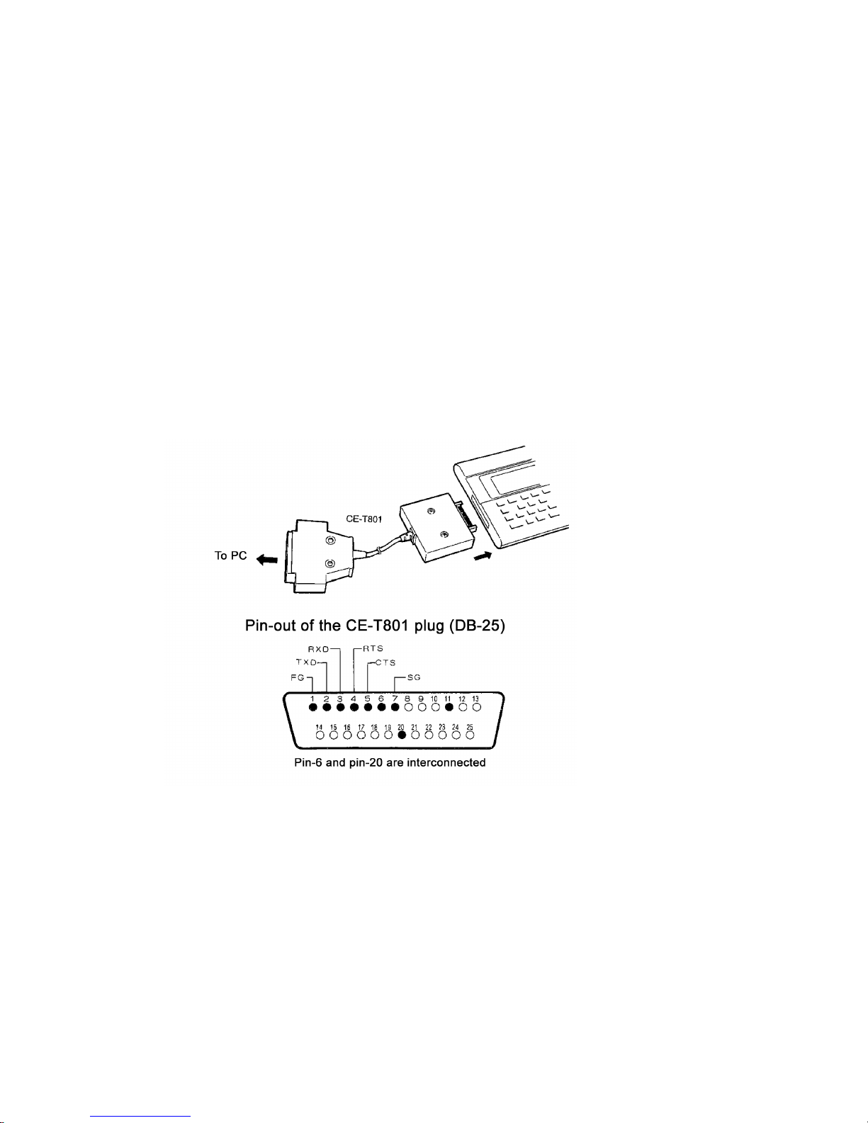
SIO-Mode:&Data&Transfer&Cable&CE-T800&and&CE-T801&
!
The data transfer cables CE-T800 and CE-T801 are RS-232 level converters with an
integrated null-modem wiring. They can be used to connect the PC-G850V(S) to a
personal computer (PC) or other devices.
With these cables you can transfer data, program source-code or machine language
programs from or to a PC by using the TEXT/Sio-submenue or the SIO-commands (R,
W) of the integrated hex-monitor (MON). The DB-25 plug of the cable can be connected
directly to a PC (if necessary via a DB-9 adaptor), when there is a physical COM port.
Alternatively it can be connected to a USB-port through an additional serial-to-USB
adaptor. Don't use a null-modem adaptor or wiring for a PC-connection (because it's
already integrated in the cable).
However if a peripheral RS-232 device like the 4-color plotter CE-515P shall be
connected, a null-modem adaptor/wiring is mandatory in order to compensate the
integrated one.
On the CE-T800 pins 6 and 20 are not connected, pin 11 is not connected on both
models (CE-T800 and CE-T801).
Attention: Never touch the pins of the DB-25 plug. Static electricity may be harmful for the
circuits.
A free working area of about 300bytes is required for data transfer from a PC.
!
&
Page 8

SHARP&PC-G850V(S)&&&User&Manual&-&&Appendix!A:!11-Pin!Interface&
!
8!
SIO-Mode:&USB&PC-Adaptor&Cable&with&Hardware-Handshake&&
!
An elegant, hence powerful DIY-alternative for the connection of the PC-G850V(S) with a
modern PC is based on a pre-built USB-UART adaptor cable with open endings.
Specification:
FTDI USB-UART/TTL adaptor cable based on FT232R-chip, 5V, 6 pins
(GND,5V,RXD,TXD,RTS,CTS)
For physical connection with the 11-pin interface of the PC-G850V a common multi-pinconnector with 2.54mm spacing can be used. You need to solder the UART-lines of
adaptor to the multi-pin-connector by using a null-modem wiring then:
FTDI-UART
Signal (Color)
PC-G850V(S)
Signal (Pin)
GND (black)
GND (3)
RXD (yellow)
TXD (7)
TXD (orange)
RXD (6)
CTS (brown)
RTS (4)
RTS (green)
CTS (9)
VCC (red)
-
Additionally there should be a 10kOhm resistor between pin-4 and pin-3 of the multi-pinconnector. It serves as a pulldown for the RTS-signal, to get a defined LOW level.
Without it, you might experience I/O-errors when transferring data from a PC to the PCG850V(S), because the PC may not receive wait requests from the pocket computer.
Finally you have to download the tool FT_PROG from the website of the manufacturer:
www.ftdichip.com. With this tool you must logically invert the signals RXD, TXD, RTS and
CTS of the FTDI-chip, because the SIO-mode (RS-232 interface) of the PC-G850V(S)
operates on inverted UART-logic (see above). This is a one-off process and the settings
are persisted within the integrated EEPROM of the FTDI-chip.
Page 9

SHARP&PC-G850V(S)&&User&Manual&-&Appendix!A:!11-Pin!Interface&
!
9!
SIO-Mode:&RS-232&Printer&
With the SIO-mode you can also make use of printers that provide an RS-232 interface,
like the 4-color plotter CE-515P or CE-516P.
Do not connect an RS-232-printer to the PC-G850V(S) without a voltage level converter!
The data transfer cable/converter CE-T800/801 can be used in combination with a nullmodem wiring or adaptor. To connect the CE-515P/516P via RS-232 a DIN-4 plug is
needed. The correct wiring (inluding null-modem) is as follows:
Be sure to have the DIP-switches on the back side of the CE-515P/516P configured
correctly (see printer manual for details).
Furthermore you have to adopt the RS-232 parameters in the TEXT/Sio/Format submenue of the PC-G850V(S) in order to get a connection with the CE-515P:
• baud rate = 1200
• data bit = 8
• stop bit = 1
• parity = none
• end of line = CR
• flow = RS/CS
Now, to actually direct outputs to a RS-232-printer, you have to open the 11-pin interface
explicitely in SIO-mode (OPEN“COM:“) – and close it after use (CLOSE). Characterstrings and control codes are transmitted via the PRINT#1,“...” command in
between.
OPEN“COM:“
PRINT#1,“HELLO WORLD“
…
CLOSE
The commands LPRINT, LLIST, LFILES however are not routed to the 11-pin interface
in SIO-mode.
!
&
DIN-4 Plug
CE-T800/1 DB-25 Plug
Pin#
Signal
Pin#
Signal
1
+12V
-
-
2
BUSY#
4
RTS
3
GND
7
GND
4
DATA#
3
RXD
Page 10

SHARP&PC-G850V(S)&&&User&Manual&-&&Appendix!A:!11-Pin!Interface&
!
10!
SSIO-Mode&&
!
The SSIO-mode serves for the purpose of synchronous serial data transfer – in contrast
to the asynchronous serial data transfer of the SIO-mode. “Synchronous” means, that the
sender provides an additional strobe/clock signal, to which the receiver aligns. This
makes an explicit baud-rate obsolete, to which both sides have to be configured in SIOmode. Hence the settings of the TEXT/Sio/Format-submenue are irrelevant in SSIOmode.
The SSIO-mode provides different submodes resp. protocols.
SSIO-Mode:&CE-126P&Print&Protocol&
!
This is the default protocol for the 11-pin interface of the PC-G850V(S). It is the protocol
for the printer CE-126P and it is active if and only if there is no other (sub-)mode
selected. The commands LPRINT, LLIST and LFILES are routed to the printer in this
mode.
The integrated cassette interface of the CE-126P can also be used by the PC-G850V(S)
and the respective protocol shares the handshake with the print protocol, but it uses
PWM for data transfer instead of SSIO (see below).
The pin-out and signal semantics within the CE-126P print protocol is as follows:
Pin
#
Signal
Direction
Semantics
4
BUSY
Out
Clock pulse for synchronous, serial data transmission
5
DOUT
Out
Data line
6
XIN
In
No function
7
XOUT
Out
HIGH: CE-126P sub-device select (i.e. printer vs.
cassette interface) resp. command transfer
LOW: Idle or data transmission
8
DIN
In
No function
9
ACK
In
CE-126P ready to receive data or commands
(handshake)
10
EX1
In
No function
11
EX2
In
No function
Page 11

SHARP&PC-G850V(S)&&User&Manual&-&Appendix!A:!11-Pin!Interface&
!
11!
The following diagram shows the signal timing for the command LPRINT"X" with the CE126P connected:
The PC-G850V(S) is waiting for ACK going HIGH before BUSY is set to HIGH for each
clock pulse. This synchronous, serial protocol is also used by the CE-126P interface of
the PC-E500(S).!
SSIO-Mode:&LPRT-Protocol&and&Mini-I/O&Port&
!
The mini-I/O port of the PC-G850V(S) is just a logical grouping of the six main signals of
the SSIO-mode into two groups, three signals/bits each:
• Mini-I/O output-port (3-bit)
o XOUT (bit-0)
o DOUT (bit-1)
o BUSY (bit-2)
• Mini-I/O input-port (3-bit)
o ACK (bit-0)
o DIN (bit-1)
o XIN (bit-2)
The bits of the mini-I/O port can be controlled explicitly via the functions
OUT/miniput() and INP/miniget(), so that e.g. custom communication protocols
can be implemented on that basis.
Besides that, the PC-G850V(S) provides a synchronous, serial protocol for data transfer
to a respective peripheral device. In order to enable that, the 11-pin interface must be
opened with the command OPEN(“LPRT:“). The data-streams of the commands
LPRINT, LLIST and LFILES are then sent over this protocol using ASCII code.
Page 12

SHARP&PC-G850V(S)&&&User&Manual&-&&Appendix!A:!11-Pin!Interface&
!
12!
The signal semantics of the LPRT-protocol is as follows:
Pin
#
Signal
Direction
Semantics
4
BUSY
Out
Frame-indicator for each transmitted byte
5
DOUT
Out
Data line
7
XOUT
Out
Clock pulse with pause after each byte
9
ACK
In
LOW: Receiver ready
HIGH: PC-G850V(S) must wait
The next diagram shows the signal timings:
Data is transferred byte-wise with MSB-first. DOUT is valid at the rising edge of the clock
pulse. The BUSY-signal provides an additional reference frame for each byte.
PWM-Mode:&CE-126P&Tape&Protocol&
!
This protocol is activated by the commands BSAVE, BSAVEM, BLOAD, BLOADM,
BLOAD? when a CE-126P (or compatible cassette interface) is attached in order to store,
load or verify BASIC programs or binary data sections (e.g. machine language programs)
to / from a tape recorder like the CE-152.
The protocol includes the SSIO-handshake of the CE-126P printer protocol but the actual
data transfer is realized via pulse width modulation (the digital equivalent of analog
waveforms). So it’s a kind of mixed SSIO/PWM-protocol.
Page 13

SHARP&PC-G850V(S)&&User&Manual&-&Appendix!A:!11-Pin!Interface&
!
13!
This is the signal-semantics within the CE-126P tape protocol:
Pin
#
Signal
Direction
Semantics
4
BUSY
Out
Clock pulse for synchronous, serial handshake
5
DOUT
Out
Data line for handshake
6
XIN
In
PWM data from the cassette interface (load)
7
XOUT
Out
Handshake: See CE-126P printer protocol
Data: PWM transfer to the cassette interface (save)
8
DIN
In
No function
9
ACK
In
CE-126P ready to receive data or commands
(handshake)
The following diagram shows the signal timing of the CE-126P tape protocol for a
BSAVE-operation (saving a BASIC-program with only one line):
!
!
The dynamics for a BLOAD-operation is equivalent, but the PWM-data is received
through the XIN-signal then.
PWM-Mode:&Generic&PWM-Protocol&
!
This protocol is equal to the CE-126P tape protocol reduced to XOUT and XIN. It is
activated by the commands BSAVE, BSAVEM, BLOAD, BLOADM, BLOAD? when no
CE-126P (or compatible cassette interface) is connected. Typically this would be the
case, if two PC-G850V(S) are directly interconnected by a cross-wired cable like the EA129C. The PC-G850V(S) distinguishes the activation of the CE-126P tape protocol from
the generic PWM protocol by setting XOUT to HIGH as the very first action for a
BSAVE/BLOAD-command: If ACK is not going HIGH then, the generic PWM-protocol is
used (i.e. BUSY/DOUT/ ACK handshake being skipped).! &
Page 14

SHARP&PC-G850V(S)&&&User&Manual&-&&Appendix!A:!11-Pin!Interface&
!
14!
PIO-Mode&
!
The PIO-mode is primarily intended for the purpose of controlling external digital
hardware, rather than for data communication with other devices. With this mode you
change the pocket computer into a microcontroller with an on-board development
environment.
The 11-pin interface becomes a programmable 8-bit port. The logic levels (LOW/HIGH)
can be set and read by the PIO-API (API = Application Programming Interface) in BASIC
or C. Each of the 8 signals/bits can be configured individually to serve as input or output.
The direction can be set by the function pioset/PIOSET (see command reference).
The function pioput/PIOPUT sets the individual logic levels of each signal by setting
the respective bit to 0 (=LOW) or 1 (=HIGH). Signals that were configured as input are
ignored then. The function pioget/PIOGET reads all 8 logic levels of the port into one
byte.
In order to demonstrate the PIO-mode usage, here is a very simple example:
In this example bit-0/pin-4 is an output, which lights up an LED when it is in the HIGH
(logic 1) state. Bit-1/pin-5 on the other hand serves as an input that represents the state
of a push button switch. An open input (i.e. undefined level) is internally pulled down and
thus interpreted as logic 0. This is the case, if the push button is open. In order to
distinguish that state from the closed state, the push button is connected to VCC (i.e.
HIGH/logic 1) on the other side and not to GND.
Let the goal of the “microcontroller”-code be to switch on the LED by the first button-click
and to switch it off again by the next button-click (and so on). Let us use the
programming language C for this example – BASIC would be similar, but less structured.
Page 15

SHARP&PC-G850V(S)&&User&Manual&-&Appendix!A:!11-Pin!Interface&
!
15!
The following C-program implements these requirements:
1 #define BOOL char
2 #define TRUE 1
3 #define FALSE 0
4 #define BTN 0x02
5
6 char BTNstate = 0;
7 char LEDstate = 0;
9
10 BOOL setupPIO() {
11 if(!fopen("pio","a+")) {
12 printf("can't open port\n");
13 return FALSE;
14 }
15 pioset(BTN);
16 return TRUE;
17 }
19
20 BOOL pressed() {
21 BOOL rtn=FALSE;
22 char btn;
23 btn=pioget()&BTN;
24 if(btn && BTNstate==0)
25 rtn=TRUE;
26 BTNstate=btn;
27 return rtn;
28 }
29
30 toggleLED() {
31 LEDstate=!LEDstate;
32 printf("LED=%x\n",LEDstate);
33 pioput(LEDstate);
34 }
39
100 main() {
101 printf("PIO test\n");
102 if(!setupPIO())
103 abort();
104 while(TRUE) {
105 if(pressed()){
106 printf("button pressed\n");
107 toggleLED();
108 }
109 }
110 }
To enter the symbol '\' press -G in TEXT-Mode. It is displayed as .
Page 16

SHARP&PC-G850V(S)&&&User&Manual&-&&Appendix!A:!11-Pin!Interface&
!
16!
Comments on the code:
• Line 4: Bit-mask for bit-1 (0b00000010), i.e. push button input
• Line 6: Global state variable for the push button
• Line 7: Global state variable for the LED
• Line 11: The interface is opened in PIO-mode for read and write.
• Line 15: Configure bit-1 / pin-5 as input. All other signals are outputs.
• Line 20: This function detects the transition from bit-1 = 0 to bit-1 = 1, i.e. the close
event of the push button.
• Line 23: The PIO-port is read and all bits are masked out, except bit-1.
• Line 30: This function changes the state of the LED.
• Line 33: The new LED-state (bit-0) is written to the port.
Unused outputs are set to 0.
• Line 104: Main-loop, abort by ON/BREAK-key.
The following images show an experimental setup and the respective trace outputs on
the display of the PC-G850V.
Page 17

SHARP&PC-G850V(S)&&User&Manual&-&Appendix!A:!11-Pin!Interface&
!
17!
PIC-Mode&
!
The PIC-mode of the PC-G850V(S) is used for the transfer of an assembled PICprogram to a PIC microcontroller. This process is called PIC-programming, PIC-program
(up)loading or PIC-burning, since a specific “burning” voltage is needed that is much
higher than normal operating voltage. This mode is activated by the PIC-loader menue
item in the PIC-assembler sub-menue only. The PC-G850V(S) supports the ICSPprotocol (In-Circuit Serial Programming) of the PIC16F8x microcontroller family and
compatible models.
The pin-out and signal semantics of the 11-pin interface in PIC-mode is as follows:
Pin
#
Signal
Direction
Semantics
4
CP
Out
This signal controls the ICSP-programming mode of the
PIC. If this signal is HIGH, the burning voltage (+12 to
+14V) must be provided at the MCLR#-pin of the PIC.
If this signal is LOW, the MCLR#-pin must be at GNDlevel or VDD (+5V).
5
CLK#
Out
This signal provides the ICSP-clock-pulse for the PIC to
be programmed. However the inverted CLK# (i.e. CLK)
signal must be provided at the RB6-input-pin of the PIC.
The latter latches data bits on the falling edge of that
CLK-pulse.
6
DATAIN
In
This input must be connected with the RB7-pin of the
PIC. Data is read from the PIC over this line for
verification of the programming process.
7
DATAOUT
Out
This output is used for serial data and command transfer
to the PIC in ICSP-mode. It has to be connected with the
RB7-pin of the PIC too.
8
LOWBATT#
In
This digital input can be connected to a programming
voltage monitoring circuit (esp. when using an external
supply). LOW (logic 0) means „weak voltage supply“.
Due to the specification of the PIC16F8x family, the PIC performs a transition to ICSPmode, if and only if all of the following conditions are true:
• VDD = +5V, VSS = GND
• MCLR# = +12V to +14V
• RB6 (CLK) = LOW.
• RB7 (DATA) = LOW.
Page 18

SHARP&PC-G850V(S)&&&User&Manual&-&&Appendix!A:!11-Pin!Interface&
!
18!
The following image shows the pin-out of a PIC16F84A as a representative:
&
&&&&&&&& &
The PIC-loader of the PC-G850V(S) supports the ICSP-protocol as stated above, but
preceding to that there is a connection test phase. If it fails, the programming process
stops and the message Connection error! is shown on the display.
In order to get into more details of the PIC-loader dynamics, we take a minimalistic
example code for the PIC16F84A. It just consists of the configuration word and an infinite
loop without body:
10 #include ”p16f84a.inc”
20 __config 0x3ff6
30loop goto loop
The PIC-assembler compiles this source code into a PIC machine language program
with only one PIC-word (14-bit). The next diagram shows the phases of a successful
burning process controlled by the integrated PIC-loader of the PC-G850V(S):
CLK was strobed at the RB6-input of the PIC (i.e. the already inverted CLK# signal). DATA was stobed at
the RB7-pin. CP directly controls the programming voltage at the MCLR#-pin.
Page 19

SHARP&PC-G850V(S)&&User&Manual&-&Appendix!A:!11-Pin!Interface&
!
19!
1. Connection test: The PC-G850V(S) sets DATAOUT to HIGH and checks, whether
DATAIN is going HIGH as well. So both signals have to be connected, otherwise
the ICSP-protocol will not be activated!
2. This is the ICSP-phase, entered by MCLR# = 12,5V, CLK = LOW, DATA = LOW.
a. Writing the assembled 14-bit word (PIC-op-code)
b. Verification (read) of the last programmed PIC-op-code
c. Increment the PIC program counter. If the PIC-program consisted of more
than one word, there would be a 2a/b/c loop for every other word.
d. Writing the PIC-configuration word
e. Verification of the PIC-configuration word
This diagram is a zoom-in of phase 2a:
&
PIC-ICSP commands are 6-bit wide (see specification of your PIC). A command can be followed by a data
word – writing or reading. Data words are 14-bit wide, but they are framed by a start- and a stop-bit, so that
there are 16-bit in total. Transmission is done always with the least significant bit first (LSB-first). All bits are
latched/provided at the falling edge of the CLK-pulse, as already mentioned.
&
1. PIC-ICSP command „Load Data for Program Memory“ (0x02).
2. Data transmission for the „Load Data for Program Memory“-command. So in this
example the 14-bit op-code compiled by the PIC-assembler is 0x2800.
3. PIC-ICSP command „Beginn Programming Cycle“ (0x08). This command has no
data parameter and starts the PIC-internal burning process for the latched 14-bit
word.
&
Page 20

SHARP&PC-G850V(S)&&&User&Manual&-&&Appendix!A:!11-Pin!Interface&
!
20!
Now an appropriate PIC-burner circuit for the 11-pin interface of the PC-G850V(S) is
needed, that utilizes the integrated PIC-loader and supports the PIC16F8x
microcontroller family. Such a circuit must match the follwing criteria at least:
1. The CP-signal must control the programming/burning voltage for the PIC.
2. DATAIN and DATAOUT must be interconnected already for the connection-test
phase.
3. The inverted CLK#-signal must be provided at the RB6-pin of the PIC.
4. The CLK#-signal is very sensitive for cross-talk – especially from DATOUT.
Shielding and/or elemination of interference can be necessary. Furthermore a
pulldown resistor is needed for a defined LOW-level of the CLK#-signal.
5. The LOWBATT# input must either be connected to a programming voltage
monitoring circuit or pulled up to the HIGH-level.
The following circuit meets these requirements. An additional feature is that it does not
need an external power supply providing the programming voltage, but it creates this via
a DC/DC-converter from VDD (+5V):
A +5V to +12V DC/DC-converter like the TMA0512C (or ~D) can be used to provide the burning voltage.
The CP-signal controls this as VPP for the MCLR#-pin through the transistors T1 and T2. The LED serves
as an indicator for ICSP-mode. T3 and R8 are inverting the CLK#-signal which then is connected as CLK to
the PICs RB6. C2 (as a low-pass filter) works for interference elemination at the CLK-signal if necessary.
The low voltage indicator only raises an exception, if the operation voltage supply falls below the LOWthreshold (i.e. logic 0) during the programming phase.
Page 21

SHARP&PC-G850V(S)&&User&Manual&-&Appendix!A:!11-Pin!Interface&
!
21!
In order to test the complete PIC programming process with the PC-G850V(S), the
following, quite simple PIC-program can be used. It flashes an LED that is connected to
the RB1-pin:
10 #include "p16f84a.inc"
20 __config 0x3ff1 ;CP_OFF & PWRT_ON & WDT_OFF & XT_OSC
30DELAY1 equ 0x08 ;delay counter 1
40DELAY2 equ 0x09 ;delay counter 2
50 org 0
99
100start
110 bsf STATUS,RP0 ;change to bank 1
120 bcf TRISB,1 ;enable RB1 for output
130 bcf STATUS,RP0 ;back to bank 0
140loop
150 bsf PORTB,1 ;RB1=1,LED=on
160 call delay
170 bcf PORTB,1 ;RB1=0,LED=off
180 call delay
190 goto loop
299
300delay
310 movlw 255
320 movwf DELAY1
330 movwf DELAY2
340dloop
350 decfsz DELAY1,f
360 goto dloop
370 decfsz DELAY2,f
380 goto dloop
390 return
Enter this source code in TEXT-mode and compile it with the PIC-assembler. Now
connect a PIC16F84A with the PIC-burner circuit from above (or equivalent) to the 11-pin
interface of the PC-G850V(S). Finally activate the PIC-loader from the PIC-assembler
sub-menue.
Page 22

SHARP&PC-G850V(S)&&&User&Manual&-&&Appendix!A:!11-Pin!Interface&
!
22!
After successful program upload, decouple the PIC from the burner circuit and install it
within the following test circuit:
This test circuit utilizes an external quarz < 4MHz as a clock. That corresponds to the
setting of XT_OSC within the configuration word (0x3FF1) of the sample program (see
specification of the PIC16F84A).
If the PIC has been programmed correctly, the LED will start flashing as soon as a power
source (+5V) is connected to the test circuit. The push button switch is optional and
brings the PIC into RESET-state when pressed (MCLR#=LOW). Program execution is
halted then, so the LED is permanently off. The flash frequency can be influenced via
quarz-frequency selection (hardware) or by changing the number of iterations of the outer
delay loop (software) in line 310 of the sample program, range 1..255.
&
 Loading...