

Page 1
PC9D10
PC9D10
Ultra-high Speed Response,
2-channel OPIC Photocoupler
■ Features
1. Built-in 2-channel
2. Ultra-high speed response
(t
PHL
: TYP. 50ns at R
, t
PLH
= 350Ω
L
3. Isolation voltage between input and output
(V
: 2 500V
ISO
4. Low input current drive (I
)
rms
: MAX. 5mA
FHL
5. Instantaneous common mode rejection
voltage (CM
: TYP. 500V/µs)
H
6. Recognized by UL. file No. 64380
)
)
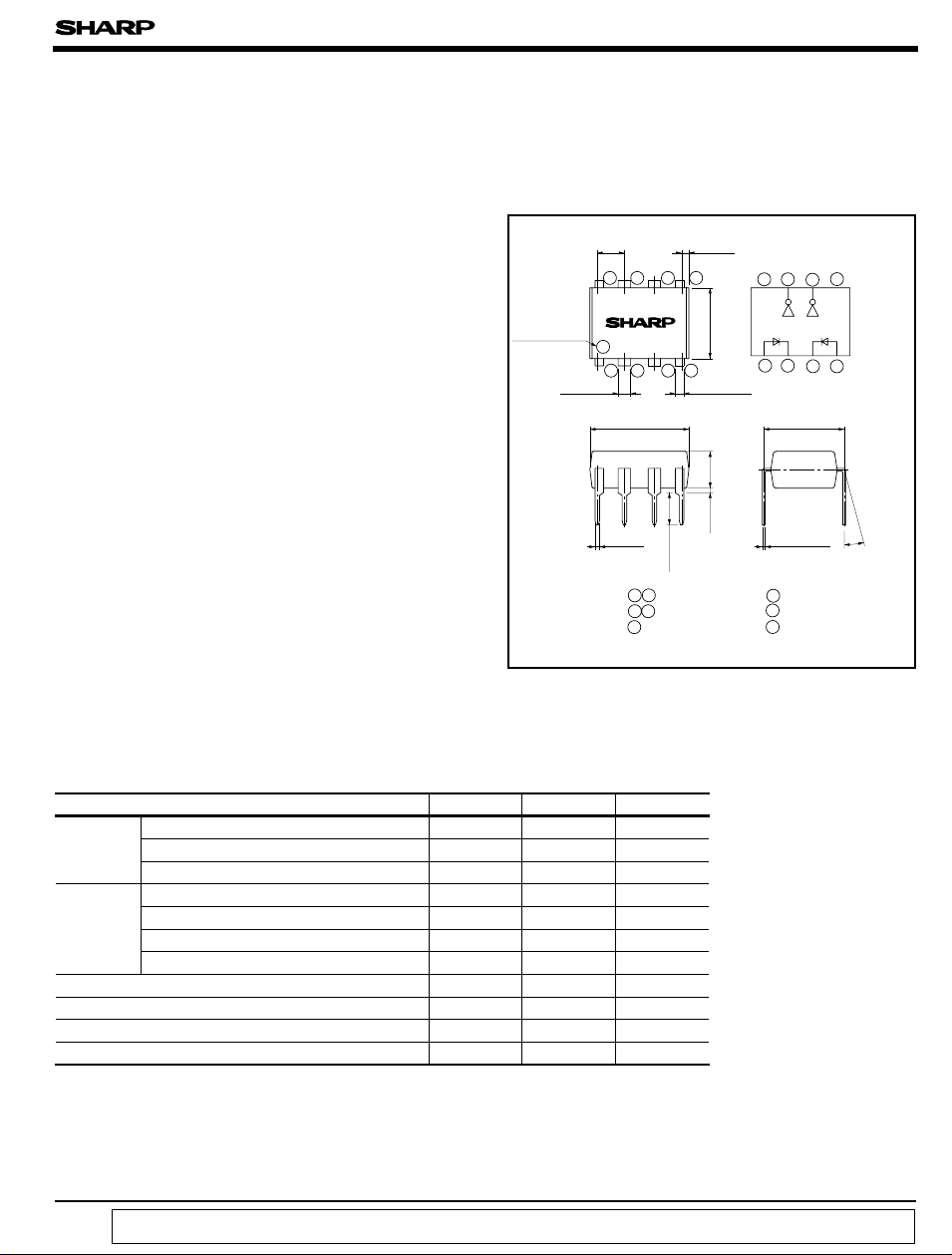
■ Outline Dimensions
± 0.25
2.54
Primary side mark
(
)
Sunken place
± 0.3
1.2
PC9D10
12 34
9.22
0.8
5678
0.85
± 0.5
■ Applications
1. Computer perpherals high speed interface
for microcomputer systems
2. High speed line recievers
3. Digital audio equipment
4. Interface with various data transfer equipment
*Output sides are open collector.
* “OPIC ” (Optical IC) is a trademark of the SHARP Corporation.
An OPIC consists of a light-detecting element and signal processing circuit integrated onto a single chip.
■ Absoulte Maximum Ratings
Parameter Symbol Rating Unit
*1 *2
Forward current I
Input
Output
*2
Reverse voltage V
*1 *2
Power dissipation P 40 mW
*3
Supply voltage V
*2
High level output voltage
*2
Low level output current
Collector power dissipation
*4
Isolation voltage V
Operating temperature T
Storage temperature T
*5
Soldering temperature T
*1 Ta= 0 to 70˚C
*2 Each channel
*3 For 1 minute max.
*4 AC for 1 minute, 40 to 60%RH. Apply the specified voltage between the whole of the electrode pins on the input
side and the whole of the electrode pins on the output side.
*5 2mm or more away from the lead base for 10 seconds or less
F
R
CC
V
OH
I
OL
P
C
iso
opr
stg
sol
15 mA
16 mA
60 mW
2 500
0 to + 70 ˚C
- 55 to + 125
260 ˚C
± 0.1
0.5
± 0.5
3.0
1 4 Anode
2 3 Cathode
5 GND
(
Ta= 25˚C
)
5V
7V
7V
V
rms
˚C
± 0.2
± 0.5
6.5
± 0.3
± 0.5
3.5
TYP.
0.5
(
Unit : mm
Internal connection
diagram
5678
1234
± 0.3
7.62
± 0.1
0.26
θ : 0 to 13 ˚
6 V
02
7 V
01
8 V
CC
)
θ
“ In the absence of confirmation by device specification sheets, SHARP takes no responsibility for any defects that occur in equipment using any of SHARP's devices, shown in catalogs,
data books, etc. Contact SHARP in order to obtain the latest version of the device specification sheets before using any SHARP's device.”
Page 2
PC9D10
■ Electro-optical Characteristics
Parameter Symbol Conditions MIN. TYP. MAX. Unit
Forward voltage V
Input
Reverse current I
Terminal capacitance C
High level output current I
Output
Low level output voltage V
High level supply current I
Low level supply current I
“ High→Low” threshold
input current
Isolation resistance
Floating capacitance
“ High→Low ” propagation
delay time
“ Low→High ” propagation
delay time
Response
time
Rise time, Fall time
Transfer characteristics
Instantaneous common mode rejection voltage
“ High level output ”
Instantaneous common mode rejec-
CMR
tion voltage
“ Low level output ”
I
R
t
t
t
CM
CM
■ Recommended Operating Conditions
Parameter Symbol MIN. MAX. Unit
Low level input current I
High level input current I
Supply voltage V
Fanout (TTL load
)
Operating temperature T
FL
FH
CC
N-8-
opr
Connect a ceramic by-pass capacitor (0.01 to 0.1µF) between
and GND at the position within 1cm from pin.
V
CC
0 250 µA
715mA
4.5 5.5 V
070˚C
(
Unless otherwise specified, Ta = 0 to + 70˚C
Ta= 25˚C, IF= 10mA
F
Ta= 25˚C, VR=5V - - 10 µA
R
Ta= 25˚C, V= 0, f = 1MH
t
OHVCC=VO
OLVCC
CCHVCC
CCLVCC
FHL
ISO
C
PHL
PLH
, t
r
= 5.5V, IF= 5mA, IOL= 13mA
= 5.5V, IF=0 - 14 30 mA
= 5.5V, IF= 10mA - 26 36 mA
VCC= 5V,
= 0.8V, RL= 350Ω
V
O
Ta = 25˚C, DC500V, 40 to 60% RH
Ta= 25˚C, V= 0, f = 1MH
f
Ta= 25˚C, VCC=5V
= 350Ω , CL=15PF
R
L
= 7.5mA
I
F
f
Ta = 25˚C, VCC= 5V, V
H
= 10V, RL= 350Ω, IF=0
V
CM
Ta = 25˚C, VCC= 5V, V
L
= 10V, RL= 350Ω, IF= 5mA
V
CM
= 5.5V, IF= 250µ A - 2 250 µA
O(MAX
O(MIN
)
)
=2V
= 0.8V
Z
Z
- 1.6 1.75 V
- 60 250
- 0.4 0.6 V
- 2.5 5 mA
5x10
10
11
10
- 0.6 -
Fig. 1
-5075ns
-5075ns
-3060ns
Fig. 2
100 500 - V/ µs
Fig. 2
- 100 - 500 - V/ µs
All typical values : at Ta= 25˚C, V
- Ω
CC
F
P
F
P
=5V
)
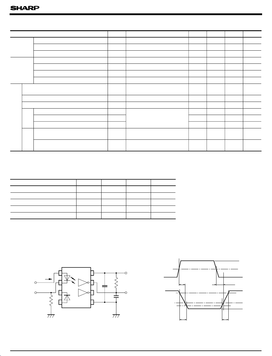
Fig. 1 Test Circuit for t
I
F
47Ω
, t
, tr and t
PHL
PLH
1
2
3
45
f
8
7
6
0.1µF
*CL includes the probe and
wiring capacitance.
350Ω
C
L
7.5mA
I
5V
V
O
F
t
PHL
90%
V
O
10%
t
f
3.75mA
PLH
0mA
5V
1.5V
V
OL
t
t
r
Page 3

PC9D10
Fig. 2 Test Circuit for CMH and CM
I
F
1
2
3
+-
V
CM
Fig. 3 Collector Power Dissipation vs.
Ambient Temperature
80
)
mW
(
60
C
40
L
350Ω
C
L
5V
V
(
I
F
V
(
I
F
V
O
= 0mA
O
= 5mA
CM
)
)
8
7
6
0.1µF
54
5V
V
V
V
10V
0V
O(MIN.
O(MAX.
OL
)
)
Fig. 4 Forward Current vs. Forward Voltage
100
)
(
mA
F
10
1
Ta= 75˚C
50˚C
25˚C
0˚C
20
Collector power dissipation P
0
0 25 50 1007570
Ambient temperature Ta (˚C
)
Fig. 5 High Level Output Current vs.
Ambient Temperature
4
)
Aµ
(
3
OH
2
1
High level output current I
0
0 255075100
Ambient temperature Ta (˚C
IF= 250µA
V
CC
V
O
)
= 5.5V
= 5.5V
Forward current I
0.1
0.01
1.0
1.5 2.0
Forward voltage VF (V
)
Fig. 6 Low Level Output Voltage vs.
Ambient Temperature
0.5
IF= 5mA
)
V
(
0.4
OL
0.3
0.2
Low level output voltage V
0.1
0 25 50 100
Ambient temperature T
(˚C
a
VCC= 5.5V
IO= 16mA
75
)
12.8mA
9.6mA
6.4mA
Page 4

PC9D10
Fig. 7-a Output Voltage vs. Forward Current Fig. 7-b Output Voltage vs. Forward Current
6
5
)
V
4
(
O
2
Output current V
1
0
Forward current IF (mA
R
1kΩ
4kΩ
= 350Ω
L
V
T
43
Fig. 8 Propagation Delay Time vs.
Forward Current
100
VCC= 5V, Ta= 25˚C
)
ns
(
80
PLH
, t
PHL
60
40
20
Propagation delay time t
0
t
=4kΩ
PLH RL
t
PLH RL
t
= 350Ω
PHL RL
Forward current I
10 155
=1kΩ
1kΩ
4kΩ
(mA
F
RL= 350Ω
CC
= 25˚C
a
)
)
=5V
5
(
Ambient Temp. Characteristics
6
5
)
V
(
4
O
R
= 350Ω
L
R
=1kΩ
L
2
Output Voltage V
1
60312
0
Forward current IF (mA
V
CC
T
a
43
=5V
= 0 to 70˚C
)
Fig. 9 Propagation Delay Time vs.
Ambient Temperature
100
I
= 7.5mA, VCC=5V
F
)
ns
(
80
PLH
, t
60
PHL
40
20
Propagation delay time t
0
0 25 50 75 100
RL=4kΩ
1kΩ
350Ω
= 350Ω
R
L
1kΩ
4kΩ
Ambient temperature Ta (˚C
t
t
PHL
5
PLH
)
)
60312
Fig. 10 Rise Time, Fall Time vs.
Ambient Temperature
250
t
r
)
200
ns
(
f
, t
r
150
R
=4kΩ
L
= 7.5mA
I
F
V
CC
=5V
■ Precautions for Use
(1)
Handle this product the same as with other
integrated circuits against static electricity.
(2)
As for other general cautions, refer to
the chapter “Precautions for Use ”
100
Rise time, fall time t
50
0
=1kΩ
R
L
t
r
RL= 350Ω
t
r
t
f
Ambient temperature T
50 1007525
= 350Ω
R
L
1kΩ
4kΩ
)
(˚C
a
 Loading...