

Page 1
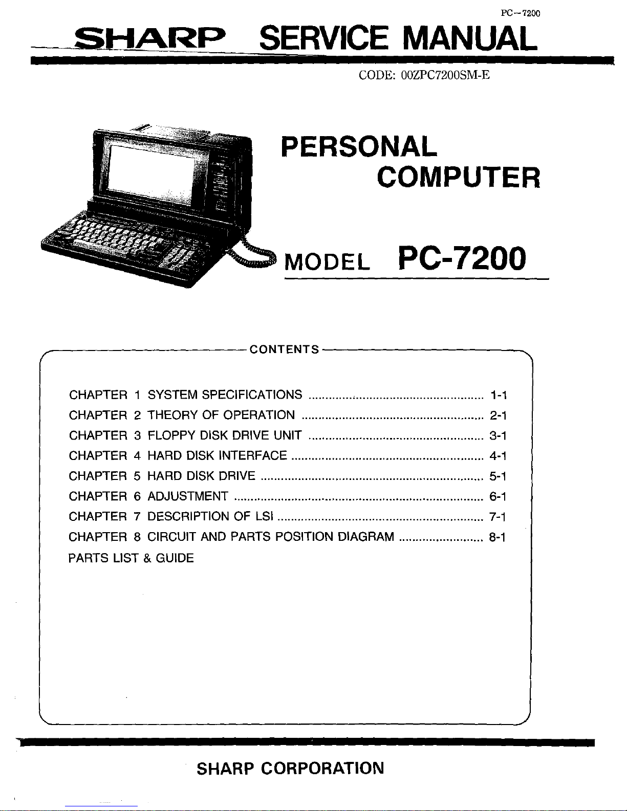
SHARP
PC-7200
SERVICE
MANUAL
CODE:
OOZPC7200SM-E
PERSONAL
COMPUTER
MODEL
PC-7200
~-------------------CONTENTS--------------------~
CHAPTER 1 SYSTEM SPECIFICATIONS ....................................................
1-1
CHAPTER 2 THEORY
OF
OPERATION ......................................................
2-1
CHAPTER 3 FLOPPY DISK DRIVE UNIT ....................................................
3-1
CHAPTER 4 HARD DISK INTERFACE .........................................................
4-1
CHAPTER 5 HARD DISK DRIVE ..................................................................
5-1
CHAPTER 6 ADJUSTMENT ..........................................................................
6-1
CHAPTER 7 DESCRIPTION OF
LSI
.............................................................
7-1
CHAPTER 8 CIRCUIT AND PARTS POSITION DIAGRAM .........................
8-1
PARTS LIST & GUIDE
SHARP CORPORATION
Page 2
I
PREFACE
SCOPE
This
manual
contains
the
theory
of
operation
for
the
PC-7200
microcomputer
system,
and
is
primarily
intended
for
service
technicians
working
in
the
field
or
in
repair
centers.
In
addition,
the
manual can
also
be
used
as
a reference document
for
technical
____
personnel
__
requirjng-
__
knowledge-~of-this-
-cdmpliteCTfis
co-il-f8i1fs-of
this
manual
are
as
simple
and
clear
as
possible,
however,
users
of
this
manual
shOUld
be
899uainted
with
computer
hardware.
About The Manual
This
manual
is
divided
into
seven
chapters:
CHAPTER
1 PRODUCT DESCRIPTION
Provides
general
information
on
the
computer
such
as
specifications
and
external
and
internal
configura-
"
tions.
CHAPTER
2 THEORY
OF
OPERATION
Describes
the
logical
and
electrical
functions
of
each
cirCuit
block.
CHAPTER 3 FLOPPY DISK DRIVE
CHAPTER
4 HARD DISK INTERFACE
CHAPTER 5 HARD DISK DRIVE
CHAPTER
6 ADJUSTMENT
CHAPTER
7 APPENDIX
NOTES: The 7200
Manual
is
generally
concerned
with
the
PC-7221
product
configuration
which
includes
the
high
density
(2HD) floppy disk drive and 20MB hard disks drive.
PC-7201/720217221
are
common
except
the
difference
showed
by
the
next
list.
The
difference from PC-7201, PC-7202 and PC-7221
PC
7201
PC
7202
PC
7221
FDD
1 x
FDD(2HD)
2xFDD(2HD) 1
xFDD
HDD
none none
1
xHDD
FDD,HDD
FDD FDD
FDD
Indicator
FDD/HDD
FDD
HDD
SPECIAL SERVICE TOOLS
PARTS CODE
PRICE
TOOL NAME
BANK
1
UKOGM2018CSZZ
_.3~
...51
(CPU.B0286)·extrac1ionlool
2 DFLP-10B3ACZZ BF
Diagnostic
media
3
DFLp·1084ACZZ
BF
Aging
test
media
1. UKDGM2D18CSZZ
o
o
2. DFLP-1 D83ACZZ
3. DFLP-1 D84ACZZ
Page 3

CHAPTER
1.
graphic character fonts.
• Standard 640K·byte O·RAM.
-
PC-7200
SVST-EM-SP-E-GlF-ICAT-ION~-
1-1. FEATURES
----
--.
-Reaf-time--eleek-{-R:r.c} . ..which storss-Jnformatioo related to the
The
PC~7200,
provided with numerous special features and
functions, can be used as a single·user or multi-user computer. It
is a powerlul office tool that can satisfy the diverse demands for
high-speed data processing and large-scale memory management
for
the
high-end personal computer
and
low-end multi-user
configuration.
80286 Microprocessor
The computer's central processing unit (CPU) has an 10MHz i6-bit
80286 microprocessor, permitting upward compatibility with 6088/
8086 processor operation. It performs versatile data processing at
a faster speed than the 8088/8086 processors.
Memory
The computer has 640K bytes of Random Access Memory (RAM)
and 64K bytes of system Read
Only Memory (ROM). ROM contains
IPL, BIOS, and diagnostic programs as well as graphics character
fonts.
LCD
Display
A large-capacity LCD with 640 x 200 pixel configuration.
Features a backlight and adjustable tilt feature for better visibility.
Built-in Interfaces
For the input/output
of
data to and from the computer, various
peripherals have been provided, including a
5-114",
high-density
floppy disk drive, a built-in
20M byte hard disk and hard disk controller
(PC-7221 only), and a RS-232C interfaces, and a Centronics-compatible printer interface.
Functional Expandability
Besides the standard features above, the functions
of
the computer
can be expanded by mounting optional devices such as the
80287
Numeric Processor Extension, or by installing any of various option
boards in the internal options slots.
Modem Card
Designed exclusively for the PC-7200, and directly attaches to the
main board.
Operating System
A DOS (Disk Operati,ng System) allows the user to communicate
with the computer and its peripheral devices, performing data
transfer and managing the memory resources of the various
equipment.
In
the single-user system configuration
of
DOS, MS-DOS version
3.2 is used. This version permits use of a wide range of commercially
available
application programs. The computer can also be run under
XENIX 286 Version (multi-user configuration) and GW-BASIC,
version 3.2.
IBM Compatibility
Most of the application software, peripherals and options designed
for the
IBM PC,
Xl,
and
AT
can also be used with the PC-7200.
1-2. SYSTEM CONFIGURATION
Figure
1-1
illustrates system architecture. As demonstrate, the
system's main components include the system unit and the keyboard
unit.
The system unit includes the main PCB, floppy disk drive, hard disk
drive (PC7221 only), and optional adapter.
The System Unit
The main PCB is composed of the following components:
• 80286 16-bit microprocessor
• Control Circuits
• 64K-byte (two
32
byte chips) ROM which contains the power-on
diagnostic program,
BIOS, initial program loader (IPL), and
1 ~ 1
system configuration and updates the date and time even if the
computer power
is
turned off.
• Keyboard interface
• Centronics-compatible parallel printer interface
• Floppy disk interface which can control up to
two
double-density
(20)
or high·capacity (2HO) floppy disk rives.
• Asynchronous serial interface which conforms to the EIA
RS·232C
standard.
• One options slots - This slot can use both IBM
PC/XT
compatible,
B·bit type. and IBM AT compatible, 16·bit type.
• A large-capacity LCD with
640x200
pixel configuration, as a
standard feature.
• Modem card designed exclusively for the PC-7200 directly
attaches to the main unit as
an
optional device.
A high density (2HD) floppy disk drive is installed as a standard
feature.
Mounted
at
the center
of
the chassis is a 3.5 inch hard disk drive
with storage capacity
of
20M~bytes.
The power supply unit has six levels
of
power output:
+5V,
-5V,
+12V,
-12V,
-15V
and AC120V. Because these voltages are
stabilized with
the
switching regulator,
the
power supply takes less
space and is light in weight.
Inside the system unit, there is a Ni-Cd battery. This battery backs
up the real time clock, permitting it to maintain information
related
to the system configuration, and to update the date and time, even
when the power is down.
SYSTEM CONFIGURATION
<
SYSTEM
u'~"CC"':....
___
~=====,--;~~-:-:
I
'.
__
•••
;1
. .
: 80287 :
L_~
_ow,
.
~
4.61'115: ',,"0"1"
~
,",e,.
0,
r===;:~~$~~:;===1
IBM
CARD
[
2"
16
b"
lull
size slots
1 " 8 bit
lull
size sici
L_-'
__
...l.
__
.L_....J
1" 8 bU
hall
size
slCI
Figure
1-1
The Keyboard Unit
The keyboard is connected to the system unit using a 6-Pin Modular
jack connector with a
coiled cable. A one chip microprocessor is
used as an interface with the keyboard unit and
the
system unit.
When the power
of
the system unit is turned on, the processor
automatically checks its
own
RAM and ROM
by
executing
the
self-diagnostic program.
Page 4
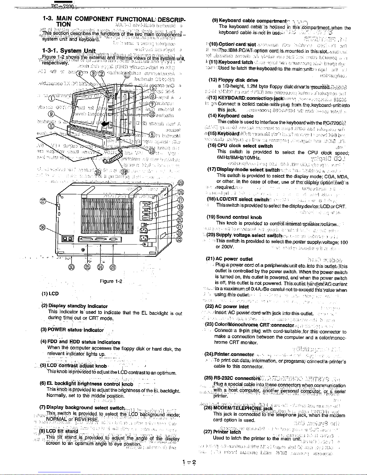
~
~~~~~~~~~~'~
..
~~~~~~~~----------------------------------------~
1·3. MAIN COMPONENT FUNCTIONAL:DESCRIP.
TION
VI;''.
-
<!
;:))'1->.);,.;.
i""';
');;
J 1
~I':
:)
)ri':
Sl
~~::~'
,;;)";
;i'·,
':-;'.-;1';)11';;
~:\:'-~'h
J'.,-':","
..
.1,
--;\
~;~'~'-'"
~~~:;
j.
__
o_,q
;J
crTh,ls,
;se~JqR
q~S_CIJQ.es-
tt"!~,
fui1GtjQns'
of
Jhe
tWd
main
~compon'ents
_
,
sySt6rri
~nJt'!inCt'
key[)oara:'1
!"),-
';
..•.
-
,;.'~;
,.'
.,'
:"-:
.. 1
;',UiJ_
,:i.;
-;;
I~:',
1
,:l-:j
-'\1"'>
•
_.
;,'),-'
-;~
L,!IJ',-~ii10;_\
,'/i3 -
'-r'):':;
··~.:n.-,.'l'-)\I
(1) LCD
,Jfr;<
-4
D:)
@i{ID
'-';:L~;XJir@;:;i_~~J~'~::);;~~;;~
:::~1:~\\:;".~~'~\
~'
-'::_-=.~~'..!J~
®1r'''
'11['
'"")
I
".J
,I_~
JJ ' I
'>®_'~I"':
<
n"*tlllr+~Jlh.:-:e-;:-j,."*l',~::::;;~::;:,,
,
;11Ulf381
.;;f1.
'~J
®,
i-'
h-d1"'''0,1
• _
".
-<,.' ,-.11".,
i-.')
'(I"
'~;~!,:;
'\;;;,'JJ
~~~b2,g=~7':""":~~l'i';~~;@._:~J""
:-1
"
Figure 1-2
(2)
Display
standby
indicator
This indicator is I
used
to
indicate that
the
EL
backlight
is
out
during
time:
out or
CRT
mgde,
(3) POWER
stalus-
indicalor
(4) FDD
and
flDD
51alus
indicalors
When
,the
computer,
i3
y
cesses' the floppy
disk'
or
hard
disk,
the
~el~vant-,in~ic_ator
lights
~p-=-
___
.
(5),t:CD'C~-~fri.~t:a(d~~t:knob"
I - J
This
knob
is-proilioed
-to
adjust the LCD contrast
to
afl
optimum.
(6) EL
backlighl
brig~lnass
COnlrol
k~Ob
• . - ,
This
k_fi(jb,-i~:ptovid~~
to
adjust the bfightness of
the
EL
backlight.
Normally, set
to
the'
iniddle'position. ' ,
,
..,
l l
(7)
Display
background
select
switCf1-'_'l',
~:,,:
"<,,,_,
_<',1
~',_''':
:,,,,.,Th[s,switch is
provided_
to
select the'Lco"bacK'grourid
'mode;
·;~"-'\NbRriAA(~r"REVER~rE.
';':
_'-J'_':~:-!j':'-j;',
:::~-',
:-""".1"
,.1,
':,-~-;-,',.J::,;:~:;;
i:".'
_,;:'J.'.
,,:,
,)--,
',:I:-'!'
:'1',"
;r,F
(SIleo
iui"'a~~
,!
',.
•...
....,',
.......
.'",
'-';
:"
."thf~
,~'n¥
sta.i1dJ~
',-provid~~i,
to
1dj~'st
'tK
e
;kngi~
'df
tli~
dfs~i~y
:,,,
"'sC-r~eii
to'~~n'bptimuh~:;angl~
jtd:~y~
~'osIt-ibh:,-1
_
':':1'",;1:-;0,'
-,-;,}
I::.
"11':
,;"
'
,',
d'-k~
1
=2
(9)
Keyboard
cable
compartment=-'
'\
"_
~
---'~',
The
keyboard -
cai)!,$.j
is-
hOJ:ised
-'in
thig::6c1mparjmep!-when
the
keyboard
cable-js-~notj
inl
use~!
!
':;;
,J,
,-
;j
~:~~i~'---;~~
,j~
:'(.10)~Option'card:5!ot,~;!-11'.1"i;jn
,:,',',
h.;''-:''J-
,;,_)~;
)'-1
Ji!-:
!!
'1':'liLThecIBMd?.G/Ali
ioptior.r'card~
is,:mounted-Jn
thrs,sJot.,~,
,;j!!
-,
" I
-1~'1
,~b;-;:;;;i.-J;)
,)-':-
)\/!;)
,l,;;
l/>'L.:i:='
li.-)
h;:;
:
~');
;-\,ti':" iU:!8';v,X!
J:l1
i
1;):Keyboarctlatch :;,,!
--'~-J,;_)i
'---Jf,
-;
i;'ll.-:'!,"
,1VFl
>i;"i-,
iJ'3~)q,~
rt!:
;)'::'
i
':Used
'f€JI:-latch
tt:'l'el
keyboaJjdl.fO
tHe,mainc,uniti.l
l-fo9"
I
:,i:r
i
(12)
Floppy
disk
drive
a 1/3-height, 1.2M byte floppy
disK;dri~e'isomou"iell.;;~c;,).,i
j'
;-{-;i
:;,:-L'jf~)'
;'1
;~;,r~
,1
j!'i;)\
itr1!!
~''-w.~?':lJ'Y
':'Jrir1-.i~
J1'.Jj'iLifT~':n
'JI:"
'(13)
KEVBOARD~conneClio~;j@Cki"""
."".
_ ..
,_
.....
33SJ3
t~
_-,?,;i
Connec;:t
';3,
cOile'd,:'cableJ,with,p!ug
,fr.om,th~..:keybQar.dj''ilrtitlrirr:lto
this
jack.
'~D~">'J:Jo:ij
D,~31>;',,;,7-:)(J':l
-d.'
~l'~J'~i
I~)--'\l;
YI,',~_::
(14)
Keyboard
cable
This
cable
is
used
to
interface
the
keyboard
with
the
R:C£72€lO;~:i
;!1,
..
:-)1'"
--,-,,~,
',);'"
S'·,,'
:'l!J:-'
':::;i';'-i
/ifj,;,,J
c,;:j.-!
1-,
'''-I'';;J
'ojl'·'
,"'i'(~5):Keyl:ioarl1~j(J,,-!;
',,'1I'lFi.')i\;i
'/rl'-)
i;.-,),,'
11
I',
,,::-.j
'-,'wi
)iXj
twc
-.1.;::;)
~.;I:;fliil')
.c-,
l;":'j
',:'
Cill-J'!
'')11_'
":-,lL-],J'
:-"1-1;0'
:,:<;j,:3
fi,
(16)
CPU
clock
select
switch
",In'
This
switch
is provided
to
select
the
CPU
clock
speed;
6MHzl8MHzll0MHz.
(1:)
0'
'--'iii:~l'i:;:'"
,;,'
"_'_J---'
~~'i',.J
,rr'
:,1,)"
,'"
;'1--'
I':~C
(17)lDisplay):inode;'seleCt:switch":;"~
'~'l
",]1.::
i-,i'~
b,'
'11,i
This
switch
is provided
to
select
the
display
mode;
CGA,
MDA,
or
other.
In
the
case of
other,
use
of
th:e:'display:opti6F1n~arcf
is
,requiredJ1:
i!J:"'i!
'J'),
!',,;:
(18)LCDICRTselectswitchc]
c,
'i,
.,;
Thisswitch.isiprovided
to
serett
thedisplaYldevic,e;'lCD_or
CRT.
(19)
Sound
conlrol
knob
This
knob
is
provided
to
co~tro~:intermat'~p-eaket'NoIUme-~
\,(20}SU'Pply-voltage;select-sWiJcf:t!:"J' i
,'j:
(',
j;-~')
)'j
•
.
-~
This
switch,
is
praIJ.ided
:to
select
the!power.--s,upplyl
voltage;
,100
or
200V. .
-.:1"';
:'~,;i-_1t'l'
"jJ.-r
(21) AC
power
outlel
:-,;
i.;
'"
)')),';
j
PlugJ8I
po...ver
cord;of,
a'
petipherals;unit
eto.,_iotd
this
:outr.e.k.:1fbis
outlet is controlled
by
the power
switch.
When
the
'power"switch
is
turned
on,
this outlet is
powered,
and
when
the
power
switch
is
off,
this outlet
is
not
powered.
This,"Qutlet
hahdles!AO current
'in
a--rnaxitnum!of
O:4A.'-!8'e
_careful',ribt-to1exce:ed
this~yarue'
When
;~singJthiSl
outlet· ',i:' '-;',
.. "
(22) AC
power
inlel
"Insert
'AO,
paW€H"l
cord,
with:
j;3.ck
,jnto;]thisIQutle.t.
,-,I' li:--;' ,
(23) ColorlMonochrom<\,CRTccanneclor
0,
. ,
Ccirinettr:a
9.,.pio
__
plug' ,with
'cord
'suitlllble-Jor-,this
!connector
to
make
a connection
between
the
computer
and
a color/monoc-
hrome
CRT
monitor.
(24):Pdntel",c;onnector:
'>
"1
.
J-
J
j':
, To print
oUt;data,',infoiTna:tion,
or,programs/cohi;1ecl-1a,printer's
cable
to
this connector.
..
i~:(~6)jMhdEMA'ElEP~'dN~:~l~c;~<_~i',j,
.'~':,
":::~;
::r,:_',',,:l',~
"",;"
'_'"
:,l
'"
1'--1,'
,,!..,
,,,,,,,1.1,,)
,)
'_J
"'::'1,;
""'\"--ji
--J,;1
ThIS
Jack
IS
connected
to
the telephone jack,
when
the
modem
card
option
is
used.
I~
.'(;,
,:qU,)
:iri',;,
i'..J"~;:
I,-,q,;,'"
;ij',:':
~,~
):/,)
:l>c!
"'J.,
",1
I--';-j'--,-,: iiE,,'),m;
i.,;;':-~l
~~nj,':::
'1],,1
:i,"
;1:,::)I:(1
__
;(~
Page 5

(28) Power
switch
The POWER switch turns the computer
on
and off. When turning
on
the
-system, itlm--the136wef-of--f.hei3er.ipR&r
...
li.---OD-fjrsUben
___
_
turn on the computer power.
(29)
Cooling
fan
Prevents the computer against excessive heat generated during
operation.
Do
not block this ventilation opening by positioning
the computer too close to a wall etc.
Keyboard Layout
EXP: USA·English
110"
III'"
III
FS
III'"
IIE~LF6
:::]
~
110'7
IIIFB
III'"
IIIFlO
III
Fll
111m
II
I
Crt
-<
r-
P"j
H=
En~
Figure 1-3
1-4. SPECIFICATIONS
The specifications below apply to the system unit and keyboard unit.
1-4-1. System Unit Specifications
Main
Logic
CPU
Processor
....
80286
Clock frequency ...
6MHzl8MHzl9.6MHz
MPX (Option)
Processor ... 80287
ROM
Element ...
27256 EP·ROM
x2
Capacity ... 64K bytes
include
IPL, BIOS, diagnostic program and graphics character
fonts
RAM
Element... MOS
LSI
256K x1
bitD·RAMx16,
64K
x4
bitD·RAM
x4
Capacity ... 640K bytes
OPTION
Element ... MOS
LSI
256K
x4
bit D·RAM
x8
Capacity ... 1 M bytes
Clock/Calendar ... HD146818 (MC146818 compatible) battery
back-up
DMA
... 7 channels (8237A·5x2)
Interrupt Level ...
15 (8259x2)
1-2. Specifications
1-2-1. Physical specifications
The physical specifications for the PC-7200 are shown below.
• Main
unit
(includes
keyboard)
(1) Dimensions
Width: 410mm (16.1")
Depth: 160mm
(6.3')
Height: 243mm (9.6")
1
-3
PC-7200
(30)
Expansion
connector
Used for connection of the expansion box.
1-3-2. Keyboard
Figure 1-3 shows the keyboard layout
forthe
PC-7200. The keyboard
has the standard QWERTY layout with 10-programmable function
keys, numeric keypad/cursor movement keys and special keys. The
three status indicators show the
ON/OFF status of the Caps
(Capitals) Lock, Num (Numeric) Lock, and Scroll Lock keys.
Page
UF
rail;]
Down
=
N=
I
,/
Lock
)--
r,-
Is--
H~
J-'-
,""
5
-
, ,
End
j
JI:"
]
(2)
Weight
Net:
7201
8.Skg (18.8 Ib)
7202 9.3kg (20.S Ib)
7021
9.Skg (21.0 Ib)
(with the keyboard)
(3)
Power requirements
• 100V type
9Q-132V AC SO/60Hz
1.0A (includes output for CE·700P)
0.8W ":l
z.
""A
T,
• 200V type
'14,.-
'if)
lulfrr
18Q-264V AC SO/60Hz
• Cable length:
2.0m (78.7")
(4)
Environment
Temperature:
•
;-
S
~
6
~
~
t;j
10 to
35
degrees C operating (50 to 95 degrees
F)
-28
to 60 degrees C storage
(0
to 140 degrees
F)
Humidity;
-
+
I-
Enter
20 to 80% operating with no condensation; up to
90%
storage
1-2-2. Component specifications and characteris-
tics
The PC-7200 consists of the following components, whose
specifications and characteristics are shown below.
• KEYBOARD
(1) Unit dimensions
Width: 4fOmm (16.1")
Depth: 182.Smm
(7.2")
Height: 37.Smm (max.) (1.S")
(2) Unit weight
1.0Skg (2.4
Ib)
(3) Coiled cable
Diameter: 1Smm (0.6")
Length:
270±10mm
coiled state (10.6±0.4")
1,500mm
stretched
state!
(4'11")
Weight:
SSg
(1.94 oz)
Page 6
(4) Style
~--
.
• Low profile
• Cylindrical key top
• Step sculpture
.
(5»
Keys , ,
,
"102keys(Lncludingthree
keyswitl)
L~P»)
;
(6)_Layout·
.~.
'"
,!,
J,'
• I "
. ,.) See
FiguJe~_t~3.
(7) LEOS
'>"
Color: Green
Key name:
U,Y,H
SW.X
F
I
I
I
B
I
,1'1:;
"Caps Lock" Maj Bloc Mai Shift Lock,
.~-l·Numi::ock"
Verr-Nu~
BlocNum
Nurii[oc~
,_
i '
____
~·~crOIl,~?Ck'"
Arretdefil
____
BI?cScorr'
~cr911
Loc/{
, (8) Rollover
N_-key
rollover _
-'('g).
Key
sw,it~h-operaiing'-fO:rce:
--
'S'Q.±30:g
: '
60±25
gc
i
--'.'
6~±25'g
• '
(10)'
KeytopPulLfoice
'I,
k!f":
,'''-~:;'
..
(11) Lifetime . .
.
3J]OO;QOO
op~ratiqns
(keys with LED)
10;000,000 operations (keys without LED)
(12)
tiitadjustment
3-6-9-
degrees-
(13)
~Iectrical
characteristics
Power
reqlJirements:
1aOmA
+ 5V
DC
'Signal
level'
TTL
•
LCD
(1)
Unit dimensions
Width: 282.5mm (11.1'1
Depth: 142mm (5.6")
Height: 9.3mm (366 mils)
(2) Unit weight
325 g
(0.717Ib)
(3) Backlight panel
Dimensions
Width: 276.5mm (10.9")
Depth: 131mm
(0,2")" • '.
Thickness: 1.3mm
(rrlax.)
(51
milsy
Weight: 55 g (1.94 oz)
(4) Effective
display size
Width:
239.96mm (9.4")
Height: 104,96mm (4.1'1
(5)
Graphic fbrinat 1
'.
Horizohtaf:
64D
dots
Vertical: 200 dots
(6)
T
exf
format
Row: 25 lines
.
6;J!'urrin::'
80·-t:har~cters/iihe
Character:
ax8
dots
(7)iCd
cohnector
20
pin
2.S4mm'-pitch'
connector
(9) Backlight connector
4-pin,
2.S-mm
pitch nylon connector
(10) Electrical characteristics
Power requirements:
0.1
mA
(max.)
130V AC (max.)
• FLOPPY DRIVE
Refer to CHAPTER 3 (page 3-1).
• HARD DISK
Refer to CHAPTER 5 (page 5-1),
, '
,
1-4
•
R$-232C,
,(1)lnterfa~~,
, .
EIA RS-232C (voltage
interface)
(2)
Transmission
method
• Asynchronous only
.'
,Fu!!_:or:h~lf:duplex"
(3) Baud
rate,
,.
.
.,
..
.
....
.,'''',
110,150,300,600,1200,2400,
48000.r
~600
(4) Data length
7
or
8 bits
(5)
Parity
"
.~-
None, even, odd
(6)
Stop bit
- :
~·--+or
2 bits
, '(,7) Connect";
25~pin
YiY
-type'
shei1)iial~
pqnnect,or
,
(8)~EI~ctri0al·characteristics
_=.§lgnaJ.level: ~ _._
,_."
...
VOL
'=
-~5V
to' -
15V
> •
VQH
T
+5Y
\0
+)sV
VIL·~
-=-3V
to·-15V·
VIM ~ ,,3\1
to,
+15V
Sf"le:
'-'-
l
te'vel
.
Data
I
VOl,~ll
)
I
VOH,
VIH
0
•
PARALLEL
INTERFACE
(1) Interface
Centronics-type interface
(2) Connector
-"
I
Congition
,
Mark'
SpacJ
2S-pin
"0"
type shell
female
connector
(3)
Electrical characteristics
';
!
Signal' level: TTl:
VIL ~ less than 0.8V
VIH =
more
than
2.0V.
VOL ~ less than
O.4V
VOH = more
than
2.4V
• SPEAKER
(1)
Size
Diameter:
29mm
(2.24")
Thickness: 6.8mm (0.74"
(2) Impedance
81l.
(3)
Variable frequency
670-3,OOOHz
(4) Input
pQwer
Rating:
O.
I W
Maximum: 0.15W
• CALENDAR
(I)
Functon
,
Cont.wl
OFF.
ON
, ,
c..',:
,co
;
• Counts
and
presents
year,
month,
date,
hour,
minute,
s~cond,
and
day
of,
the.
week
'
• Automatic correction 'for
days-per-n]qff~h
,.
•.
A.u~o.W<?Ji.c.
_I.~ap-:y~~r
90r.r~ctiqn_.,
•
BatterY
backup
-,
,
(2)
Accuracy
Mean
monthly error: ±45 s
(3) Battery
Type: 3-51 FT
',.
,.,.
Enclosed type Ni-Cd
re,c~a(gea~Ie
battery
Capacity:
..
qOm..;\H
,_
..
,. ":',."1:,-' -
.-"
Celi:
three'celis'(:i.6v) . "
Charging method:
ContinuolJ~.
,trickl~:_c~~rg~,
(4)
Charge/backup characteristics
-.'
-'
'"
-'
-/
.'
Charge
time:
SO
hours
(0
to
100%)
Backup
time:
500
hours
(approx.
20
clays)
Page 7

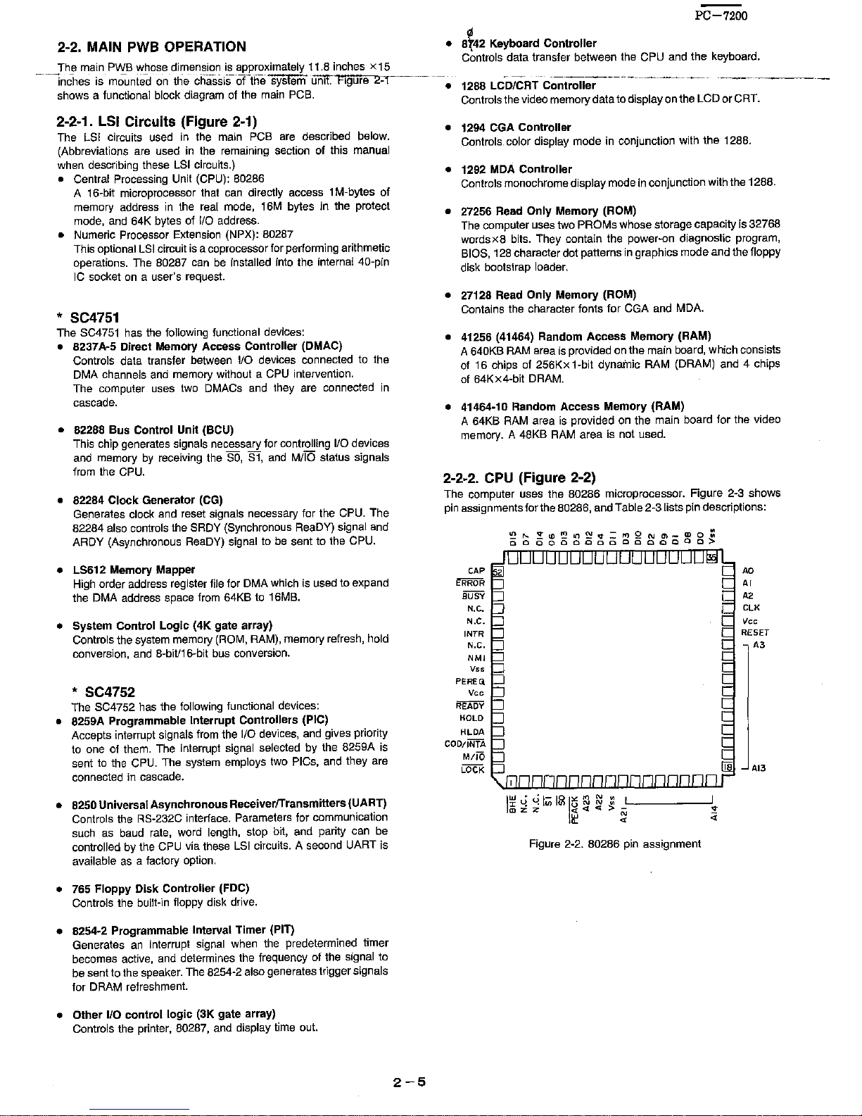
I\l
I
MAIN BOARD
HD
I/F
BOARD
~
~
~
roME
~
,---------
-----
-,
I
~
.-----------'I
MO~~
B D
§~
~
\
r--v1
(HAYE
pa~.)
0
300
bps
~
~
( 82P.36P
IBM
18
bit
BIIS
Slot)
( SZP.36P
mM
18
bit
Bus
Slot)
( 62P IBM 8
bit
Bua
Slot
)
(
62P
IBM 8 bit
BUB_
Slot
(hall)
)
I
SYSTEM LOGIC
<J[
I I
I
L
BOOB6
>or
H a
~
'bids
~
l'i
~~A
"oW>
"'''
""'"
..
,"
;--
;M/IO
6/8/10
MH,
cg~
IDGH
D"TA
BUS
..-
,
l'EAilK
015
~
~;"'f
1iUSY281 0'1
''''''''',''
"""
WI
~
110281
~~
~,~
JL
00
HOLDA
OLK
CLK286
r
~b'DY
~
~
00--"
SYSTEM
CONTROL LOGIC
8237)(2
"'"
""'"
LS612
SC4751
M-"
QIO"
fltl~
RAM
(64KB)
"",.,
DB_IS
00-7
ADD
BUS
ADD
BUS
mUH
OAT"
BUS
LOW
DATABUS
COMMANDilUS
~f-H--
'~
00--1
00--1~
M">--.
CASL.C"SHI
WE.OE
"0-8
- -
;~
,----IIF
~
i-
-
--l
_.
n I
I
3~'
~
§
• I
~
L_
,
a ...
F,a.
e1'·
...
If---
EXPANSION
BOX
T -
DiSPLAY
INTERFACE
LoGlC-
- - - - - - 1
I I
I
I
";l, I
CRTJ1:CD
I
"-'
'"-./
CRT/LCD
I
~
~
___
,
~=i)
I
I
I
,--,------fTTl
I
I
I
I
I
I
I
I
CLRIGM
110
CONTROL LOGIC
I'
PD765
ClK24M
8259)(
2
I
I
r;:::J.-",~CLK19M::
CLK14M
~
r'
I
I
I
I
I
I
I
I
I
I
I
I
""
L_
,
I
UM/seaK
I I LCD
1-
______________________________________________________
I FDD
Figure 2-1. System block diagram
I
~
go
~~
-n"'D
'-1
c:l>m
"tI::D
~~
~
a:>
f
N
,
~
,
~
!II
-<
!II
-!
m
i!:
I
m
r-
0
0
;0;
C
;;
Gl
:II
:I>
;:
~I
0
Page 8
·'"
,:i
,"--
~.
"~',
--I
-
"-
-
I ,
"
~i~--,'-
~
,.
__
:!,l
-.
;,;
'-
..
,'
_ i
;
I,
. i '
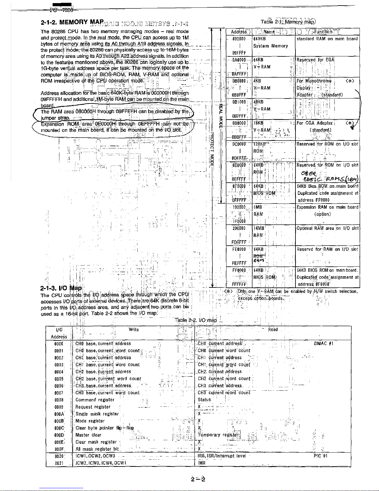
·000000
I
09FFFF
640KB
standard
RAM
on
main
board
System Memory
,
OFd~o~ ! 64~B:
,!
:'
:
i:
64KB:BioS_Ro'M_on,main
board
-
-;
'.!,
-
1'--" : ',--
B/~S'"B;o-~(-
~,Duplicated'~c~de
assignment
at
OFFFFF-
.~.
address
FFOOOO
100000
_T~
II~-
--
•.
-'
i
,
lFO.oOO
200000
I I
FD5FFF
'
FEOOOO
I
FEFFFF
·lMB
R~M
,
14MB'
R~~
61KB
'
~~~
'I~'
E~'pansion.
RAM
on
main
board
(op~ion)
Optio'nal
RAM
area
ion
I/O slot
Reservd
for-RAM
on
I/O slot
2-1-3. 1/0
Mapi'
,',.,
'!
:;
..•
;,'
!
IJ~',"
The
CPU
:cohtlr6l~ithe--;-iIO.(ad&ess,
spCJ,pejh~~:gh"wi1ic~:
t~e
C!?V!
-;
1
-<*>
~Dn,ly,\one
i,Vi-MMI
~all
be
enabled
bYIH/W
sWitch
selectIOn,
accesses
IId~ort~:bf
~ict~rhJI
d~vl¢~s.JB~-~e!arei64K"(;i'scre~e
8~b:it
:
ports
in
this
i/o;
cidtlresel"area,
and
any
adjaCent!
two
...
p-otts-can
be
:
-,:
,:;e,XG:e'pi-.op~O~:::b~a~d+·.~~
.'
~'-:~-l
used
as
a,
1e-~il
P~rt.
Table
2-2
shows.
the-.I/O
map-:"
'.
: '
-~r1~bl~
'2T?
;/O:~~~
110
Address
0000
0001
0002
0003:
0004
0005
0006
'
0007
0008
0009
OOOA
OOOB,
OOOC
0000
OOOE:
OOOF,
0020
0021
!
I:
.
,I
__
._
.•
Write
:
CHO
base,
curren~
address
:
CHd
base, curren(W:ord:
count~
;
CHI
base,Olcu-rrenf:
.;ddress
I
'~Hl
base,
9urre~tl
word count
:
t~2
base,
¢~t,r~mj
address
!
Ctb
base,
turrrent
word count
i ' I
1..
___
-'
____ . _
,.
QH3...bas.e
..
current.addiess_
--
cH"f
base
,currenf-warp 'count
, ,
Command register '
~
~,
Request register
:
Single
mask
register
Mode
register
, : !
Clear
byte painter
flipLflo~
Master clear "
Clear
mask
register
All
mask
register bit,
ICW1,GGW2,GCW3
JCW2,
ICW3,
ICW4,
OCWI
l.~",C":'
i,
'(j
I
,-
I'il
--'1
' ••
Cl;lo'
,9Ll(~ent
la~dress!
"
/,CAO'
~~i~ent
!~orcrt:6Lnt
,
:_~~t'Hl
qJr~enf
aQdress
',.'
,---
"CH'~
~~rr,eAf:$-9Jd
CO~IJ't
: ' 1
_c~:
c~rr:ent
!a~dress
I
CH2
cyr~ent
,~ord
count:
, J ~ " _
CH3.
.current
~addres.s_
'
CH3'c~r~enl
i\fora-
cou-rii' -
Status i !
X
...
~.
·X-~~
~,
.. ··,,,,'X·
" ,
X;
i
,~'
i
T'~mporary
)I'
·x
--
-
IRR"ISR-/IAter~upt
·Ievel
IMR
OMAC
#1
,"
---,
Page 9
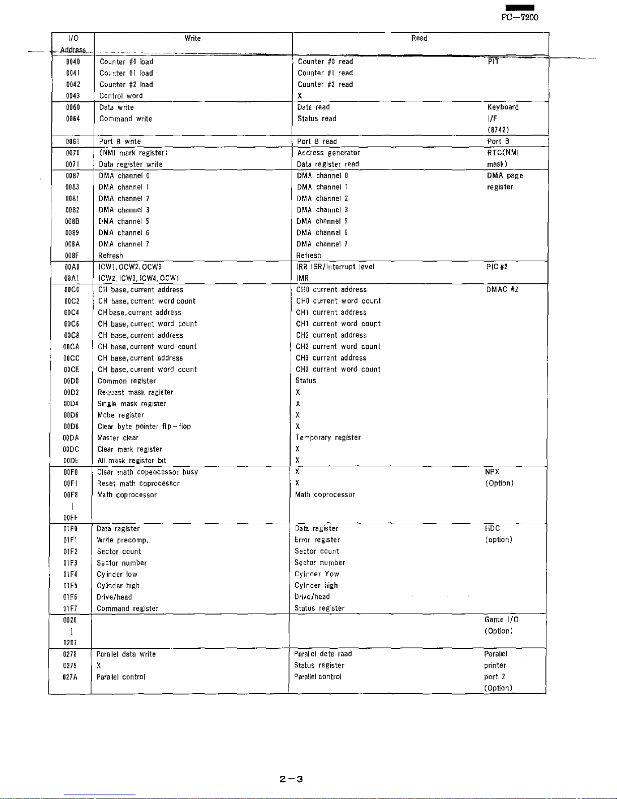
I/O
Write
_
Addr..ess_
0040
Counter
#0
load
0041
Counter
#1
load
0042
Counter
#2
load
0043
Control word
0060
Data
write
0064
Command
write
0061
Port B write
0070
(NMI mark register)
0071
Data
register
write
0087
DMA
channel
0
0083
DMA
channel
1
0081
DMA
channel
2
0082
DMA
channel
3
0088
DMA
channel
5
0089
DMA
channel
6
008A
DMA
channel
7
008F
Refresh
OOAO
ICW1,
OCW2,
OCW3
OOAl
ICW2, ICW3, ICW4,
OCWI
OOCO
CH
base,
current
address
00C2
CH
base, current word count
00C4
CH
base, current address
00C6
CH
base,
current
word
count
00C8
CH
base,
current
address
OOCA
CH
base,
current
word
count
OOCC
CH
base,
current
address
OOCE
CH
base,
current
word
count
0000
Common register
00D2
Request mask ragister
0004
Single mask
register
0006
Mobe register
0008
Clear
byte
painter flip - flop
OODA
Master clear
OODC
Clear mark
register
OODE
All
mask
register
bit
OOFO
Clear math copeocessor busy
OOF!
Reset math coprocessor
00F8
Math coprocessor
I
OOFF
01FO
Data ragister
01F1
Write
precomp.
01
F2
Sector
count
01F3
Sector
number
01
F4
Cylinder low
01F5
Cylinder high
01
F6
Drivelhead
01F7
Command register
0020
I
0207
0278
Parallel data
write
0279
X
027A
Parallel control
Counter
#0
read
Counter
#1
read
Counter
#2
read
X
Data read
Status
read
Port
Bread
Address
generator
Data
register
read
DMA
channel
0
DMA
channel 1
DMA
channel
2
DMA
channel
3
DMA
channel
5
DMA
channel
6
DMA
channel 7
Refresh
JRR,ISR/lnterrupt level
IMR
CHO
current
address
CHO
current
word
count
CHl
current
address
CHl
current
word
count
CH2
current
address
CH2
current
word
count
CH3
current
address
CH3
current
word
count
Status
X
X
X
X
Temporary
register
X
X
X
X
Math
coprocessor
Data
ragister
Error
register
Sector
count
Sector
number
Cy1.nder
Yow
Cylinder high
Drive/head
Status
register
Parallel deta raad
Status
register
Parallel control
2-3
Read
PIT
-
PC-7200
Keyboard
I/F
(8742)
Port B
RTC(NMI
mask)
DMA
page
register
PIC
#2
DMAC
#2
NPX
(Option)
HOC
(option)
Game
1/0
(Option)
Parallel
printer
port
2
(Option)
Page 10
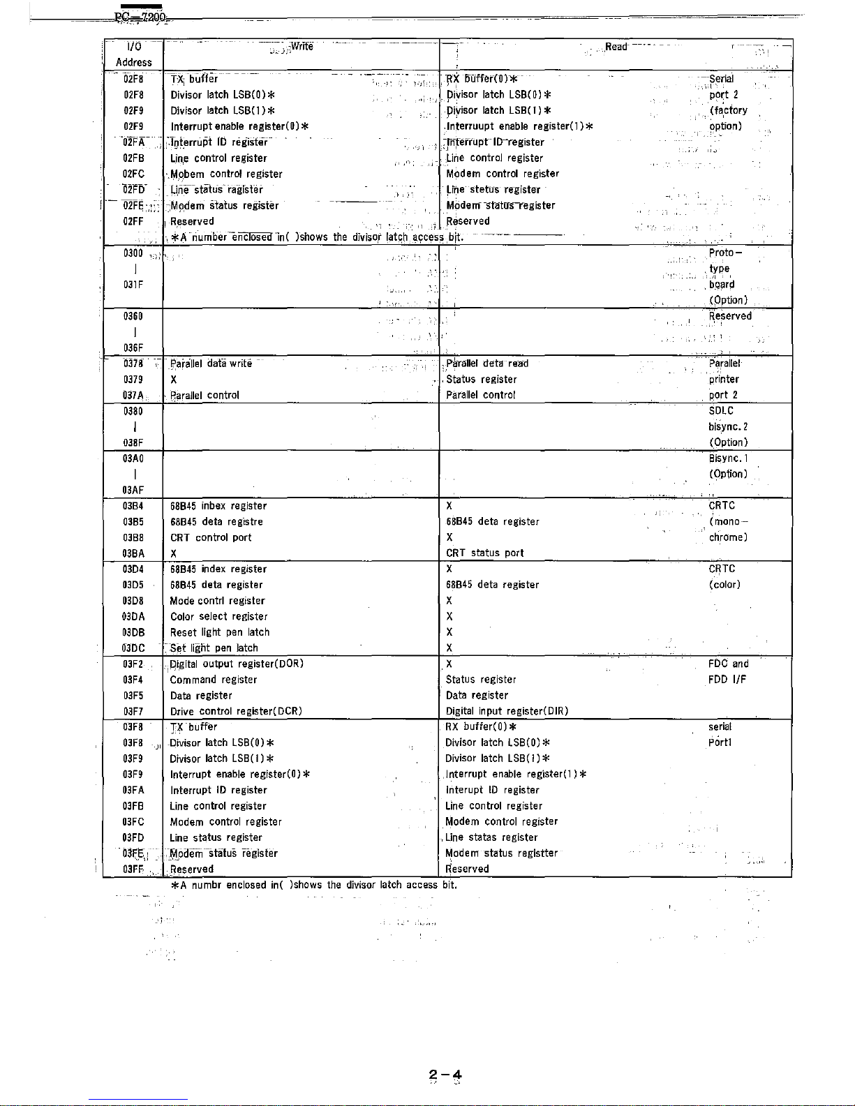
, .
I/O'
"
-
~-,-_
:
Write
.-
Read-
.,.
;
i
_1_-":,
'\1
Address
. '
02FO
-
f~
-
b-uffer
-
-
,
RX
5UII.,(0)*
.
Serial
..
':
i
"
!
I,
',',1
02FO
Divisor
latch
LSB(O)
*
•• , "J
,pivisor
latch
LSB(O)*
po~t
2
02F9
Divisor
latch
lSB(
1)
*
;
piyisor
latch
LSB
( , ) *
.'
(fa:ctory
02F9
Interrupt
enable
register(O) *
,Interruupt
enable
register( 1) *
~ption)
,
i
'olFII'
:]IJi.errupt
fD
register--
:-r-rffettupt-ID--register
,
"
i
;'11
02FB
Lin,e
control register
,
.'t,
"
: line
control
register
02FC
'-'~1Abem
control
register
Mc;ldem
control register
om)'
.
Li.ne-statu's·
ragrster
,
pr)e stetLis
-registe-r
!'-
OlF~:,1::
,--;M9,dem
status register
---_.
-
~ode
rTf
'statITS-register
i
02FF
! R,eserved
Reserved
-,
*A
-nurriber -enclasecf"in(
)shows the divisor
r~-t'~h-_:a'~ce~s
'bit.
0300
,-,'
J
:.-.
,
:
Proto
I
type
'"I,
'
031
F
,
,'.I:
'
bQard
,
,
(Option)
0360
,
~eserved
I
"
, ,
036F
, -
0310
' "
~aralJel
data write
....
,
~,P-aTallel
deta
read
Parailel
0379
X
,Status register printer
031A,
'
~arallel
control
Parallel
control port 2
0380
SDlC
I
bisync. 2
030F
(Option)
03AO
Bisync. 1
I
(Option)
03AF
,
03B4
68845
inbex register X
CRTC
,
03B5
68845
deta registre
68845
deta register
(mono-
03BO
CRT
control port
X
chro'me)
03BA
X
CRT
status port
03D4
68845
index register X
C~TC
03D5
68845
deta register
68845
deta register
(color)
03DO
Mode
contrl register X
03DA
Color select register
X
03DB
Reset light
pen
latch X
03DC
-~ ,SE!t
lignt
pen
latch
X
".
.
03F2
.JFgital output register(DOR) X
FOG
and
03F4
Command register Status
register
FDD
ifF
03F5
Data
register
Data
register
03FI
Drive control register(
DCR)
Digital input registerCDIR)
03FO
IX'buffer
RX
buffer(O) *
serial
om
"'
-Divisor latch
LSB(O)
* Divisor latch lSB(O) *
Portl
03F9
Divisor latch
LSB(
l)
*
Divisor latch
lSB(
1) *
03F9
Interrupt
enable
register(D) *
,Interrupt
enable
register(1) *
03FA
Interrupt
ID
register
[nterupt
tD
register
03FB
Line
control register
Line
control register
03FC
Modem control register
Modem
control register
,
03FD
Line
status register
,Line statas register
OltE,:
....
,';§toaem-~stiifus
re-gister
~odem
status registter
,-
J,""
03FF
,B~served
~eserved
. .
*A
numbr enclosed In( )shows
the
dIVIsor
latch access bit .
g-4
Page 11
2-2. MAIN
PWB
OPERATION
The main PWB whose dimension is approximately 11.8 inches x 15
-inches
is
mo-unted
on
the
cliassis-
onhe
system-
Urii[ Figure
2:-r--
shows a functional block diagram of the main PCB.
2-2-1. LSI Circuits (Figure 2-1)
The
LSI
circuits
used
in
the main
PCB
are described below.
(Abbreviations are used
in
the remaining section of this manual
when describing these LSI circuits.)
• Central Processing Unit (CPU): 80286
A
16~bit
microprocessor that can directly access 1 M-bytes of
memory address
in
the real mode, 16M bytes in the protect
mode, and 64K bytes of
I/O
address.
• Numeric Processor Extension (NPX): 80287
This optional
LSI
circuit
is
a coprocessor for performing arithmetic
operations. The 80287 can
be
installed into the internal 40-pin
IC
socket
on
a user's request.
* SC4751
The SC4751 has the following functional devices:
•
8237A~5
Direct Memory
Access
Controller
(DMAC)
Controls data transfer between
1/0
devices connected to the
DMA channels
and
memory without a CPU intervention.
The computer uses two DMACs and they are connected in
cascade.
• 82288
Bus
Control
Unit (BCU)
This chip generates signals necessary for controlling
1/0
devices
and memory
by
receiving the
SO,
S1,
and
MilO
status signals
from the
CPU.
• 82284
Clock
Generator (CG)
Generates clock and reset signals necessary for the CPU. The
82284 also controls the
SRDY (Synchronous ReaDY) signal and
ARDY (Asynchronous ReaDY) signal to
be
sent to the CPU.
• LS612
Memory
Mapper
High order address register file for DMA which is used to expand
the DMA address space from 64KB to 16MB.
•
System
Control
Logie
(4K
gate array)
Controls the system memory (ROM, RAM), memory refresh, hold
conversion, and 8-bitl16-bit bus conversion.
* SC4752
The SC4752 has the following functional devices:
• 8259A Programmable
Interrupt
Controllers
(PIC)
Accepts interrupt signals from the
1/0
devices, and gives
priori~
to one of them. The interrupt signal selected by the 8259A
IS
sent to the CPU. The system employs two PICs, and they are
connected in cascade.
• 8250 Universal
Asynchronous
ReceiverlTransmitters (UART)
Controls the RS-232C interface. Parameters for communication
such
as
baud rate, word length, stop bit, and parity can be
controlled by the
CPU via these
LSI
circuits. A second UART is
available
as
a factory option.
• 765
Floppy
Disk
Controller
(FDC)
Controls the built-in floppy disk drive.
•
8254~2
Programmable Interval
Timer
(PIT)
Generates
an
interrupt signal when the predetermined timer
becomes active, and determines the frequency of the signal to
be sent to the speaker. The 6254-2 also generates trigger signals
for DRAM refreshment.
• Other
110
control
logic
(3K gate array)
Controls the printer, 80287, and display time out.
2-5
PC-7200
•
8t42
Keyboard
Controller
Controls data transfer between the CPU and the keyboard.
• 1288 LCD/CRT
Controller
Controls the video memory data to display on the LCD
or
CRT.
• 1294 CGA
Controller
Controls. color display mode in conjunction with the 1288.
• 1292 MDA
Controller
Controls monochrome display mode in conjunction with the 1288.
• 27256 Read
Only
Memory
(ROM)
The computer uses two PROMs whose storage capacity is 32768
wordsx8
bits. They contain the power-on diagnostic program,
BIOS, 128 character dot patterns in graphics mode and the floppy
disk bootstrap loader.
• 27128 Read
Only
Memory
(ROM)
Contains the character fonts for CGA and MDA.
• 41256 (41464) Random
Access
Memory
(RAM)
A 640KB RAM area is provided on the main board, which consists
of 16 chips of
256Kx
l·bit
dynamic RAM (DRAM) and 4 chips
of
64Kx4·bit
DRAM.
• 41464-10 Random
Access
Memory
(RAM)
A 64KB RAM area is provided on the main board for the video
memory.
A 48KB RAM area is not used.
2-2-2.
CPU
(Figure 2-2)
The computer uses the 80286 microprocessor. Figure 2-3 shows
pin assignments for the
80286, and Table 2-3 lists pin descriptions:
CAP 2
ERROR
ausy
N.C.
N.C.
INTR
N.C.
NMI
V
..
PERE(l
READY
HOLD
HLDA
COD/INTA
M/W
AO
AI
A2
eLK
v"
RESET
A3
LOCK AI3
Figure 2-2. 80286 pin assignment
Page 12
015
-00
'I
l')ili'!Ii'l
,-
};;'~l:-r,
.'
.- -:-:'11,-,1'1
\~(
'_i~iQOJ',ti~!:Ii~c!~~;(
fi1
c~:)il
ill"'l!;
;i
,~il
ij)']';
i
j.
iJ
9H~r~ti,~.I?)
8~
Itry\t3f.~~386
begins after
,a:~fnGf'P~tO)Qr([)W}fransitiOf:i'O'f.,.·RESEl':)
;::Th'eii
HIGH
j
foJ
l:OWi;ttansiti6n
.'l~jQt
RESJ;:,Ti
:mu§tl
~;~,.~ynchronous
to
inEi'r-~¥st~iTP
cr8clf!'
1Appfoxrm~h!lyr'50'::sys1e'm
~'adCkjcYcles·
-are':requli"e-d
by
the'
CPU
for interanl initializations before
the
first
bus
cycle to
fet~R'-b;-~cba~Ef':Hm;
th-e
tp3iw'~r-'::i:in
-:
tin)
1i!'Jr"
;;-:':exec'U'ti6fii1tBcfres'S\''is
performed.
14.
Ji'"j
·)n;.;
/\.o;J )
l~YI
~tf1oj
: -)j:/V
~C6\v
1'ti
'
FifGF·fr'fr~l,sition
of
RESET
synchronous to
the
system clock will end a processor"·.c.ycle,.at
I
~
'_'">s.'&
(;\,;;
tj'"
'r;,')~;:-~~
'>.o-xni,
i"ij
:';"Ji-~~~:
~;~~~~'i~'~'~~~jJO
~OW
transiti~n
of
the
C!OCk.
·lh"~~:~-?;~:·t~
"I;l\~.Ij'
~f.'!r.~mo.n
..
~,f]1~"~-,S~T2!P;!l;}l-:P.~i:
,~
",'"
lJ
' ;li1;J.i":
,'j,]
~~',-;:T',
-,'.j;-
~:f)
;=-1nVT(
,~,a.~~~_~~~9~9~-tJ~\!r,t,
system clock,
however,{:._J[lltBiS)
casecJthcaonoJ::be~_p(e~ejer"mrne9':'Y",hl.ch;p.ha:~');!';'Slf
:;,)
':J:;;
li',";/";'
LJ)
;\',
\;-;
'j.
E ,1:-,
~)
j; --•
A9~>.pmc~~,~F!rj
QJC!c~'Jwill
occur
durinItJ,tHe':ne~f\-systeiir:clbtj{.!·per'iod}'.;Sy(rChtdr:lCiuSi
-lOW.;
to
.HIGH
,tran'sitidns
;·,q~;ij:£S;~T
:
ar~
l
,re,Q!"!!red
only for syste
ms
wh'ehjYtPle!~~roc-~:s)sOr
~'ero~l(':iri
us:tl
b'E!'
'ptia'se;,'gyrl'chrono\fsl,-to
ClK
\J"
;'-a1:-
.,'"
: ' I j ) 1 f;,
"-1'-:
~~,.
015 00
-'
51
36
'"
'
i-"
,7.:"?':
)1
1 0
-18
~
1-~.3,4-'
4, 5
another clock.
'i
b'!!:-'-l,---;, , ,
-->:'
,'J
--'<i.'\;"1:<;
L':J)
<:H-':J
~:)jj)'ilf:n:'
J:-I'
!.;
~;.,
]3:;
~~):
;\
Sys:fem~
olobk':ProYides:'the fundamental timing for
80286
systems.
It
is
divided by
two
inside''t'ri'e'
'CP'U
;
;~r
.
,i;~"'i
,-:,~
::,::;~0'~~,~,~~r~,t4
'~e,)!d,l::essor
clock.
The
internal
divide-by
two
circuitry,:-,s~9.:,qe'I~~YDch5q~i~~~~;
tp_ja_p
&Jt_e~qal
l'
-;
,:
'cloCK
)gerieratclr'jj"y a lOW to
HIGtLtr;~F);;;jti91l
.9nli,tJ1!L~~S,~)LiIlPJ-!t-..n)d
_+--,r:j;L:~
,3-)i.,j'; -"';:'
1 ,:
I/O
o
'.
Q ,
o
Data
Bus
inputs data during memory,-:I/O.' and interr.tfpt 'acknoWledge
r.ead'
cycles;,,0l:ltputs:,da_taldurjng
1
~;"D0~~
~nd
1/~"wr~~
cycles.
The
data
bus
IS
active
HIGH
and
floats to
3-state
OFF
'during!
blisnold
ackno,wle,dge.
IBlIS-'Hi~\rEnable
indicates transfer
of
data
on
the upper bytes
o't
the data bus. 015 08.
Eight-bit
.-_,1
;'
.'
,~,
__
oriented-
dev:ic8$-,
assigned to the upper bytes
of
the
data
bus
would
norn;rclUIl,:_!.l.se-'.BHEjto~con:.dition
chip
selec~,
1u,I'
nctidns.
BHE
is
active;
LGW
ahd'-floats ,ta,
3'''-,st~te
OfFliii:lurihg.
:'b~~,
·h~ld'-~~Ckri~,~;e:<;1~'~.
'o"'!I'"
'::"1--,,
" .-"n" .
I::,
1
BHE~--V:alue
" ,
'l
L
L
L
L
L
L
H
H
H
H
H
H
H
H
M/iO
L
L
L
L
H
H
H
H
L
L
H
H
H
H
BHE
and
AO
Encodings
'~);'
'J,lWord
transfe',,', ' '1:
>'"
"')jJn,~:
H Byte
translEWbn'i,upper;'h~lf
of; dati
-bus,
W1-5
~:D8'¥;
,
L Byte transfer
on
lower half
of
data bus (07 -
DO)
H Reserved
S1
so
Bus
Cycle Initiate-if"
,:J,
t
,'J
L L 1
~
h;
}')j';';
.ID~~!,r;~p,~,:..ctqMo;~}~.q,~~
J)
ld~_
':,;' ,
;. \ ..
hI!
L !:i
-IIH;
'i,'11
,R,e,~e.~v-!;!,d\"T;J"-·
H'
H"
L
L
H
H
r:_~
_'l'.d,;_
"H
Re.s,erli,ed,,1(;i
,.:;;,-.):
I!
;Ii':
,:~j:-,:
'i.l,
i
l'
',)
None,~)rrib'twa
tshitos:"cycle-"
H:;
"
"!'-::J
!~'(
I).,::
If
A 1 = 1 then halt;
els'e,Js'h'ut'doWHl
s
'~.iJ
J1J.si:,,\.---
Memory data read
Memory
data';JY{~ji.W'I~:;:\:'
'~:l'~:';it~:
:: , ..
",
::·~,;j],::./Ti
None; not a status cycle
L
II
117:1:
H
L
H
L
Res~'~'l'9]9
i~,
,!,
I
'-:,'n":>h;;
')]:j:
':,Itrj:;;~']f)~q
.l-
),B~'-;
')Hl;n;l~;tlOijr~adrjJ
JjJ~I'/v
,_;l,I,j,'
'lj!!,.',i,:
'J,'
,;'<','
)i!'JU
fPi
;,:r;'.11.1:.
'-11:J
)cll/.O-,w:r.itel'l)
;:U
",;'1.j,r:');'J:J
;;,1:.,
,lV!};-:
,_»ITHJyj
Hi
'.
p;
-'
~r
i,.'I;~,
NO'n'e;:j-rIM"ai'staiti~',;'dycle
;1.
:-,-r
':V;)
,)J
J:
'.J
-.
.-j
L L Reserved
L H
H
H H
Page 13
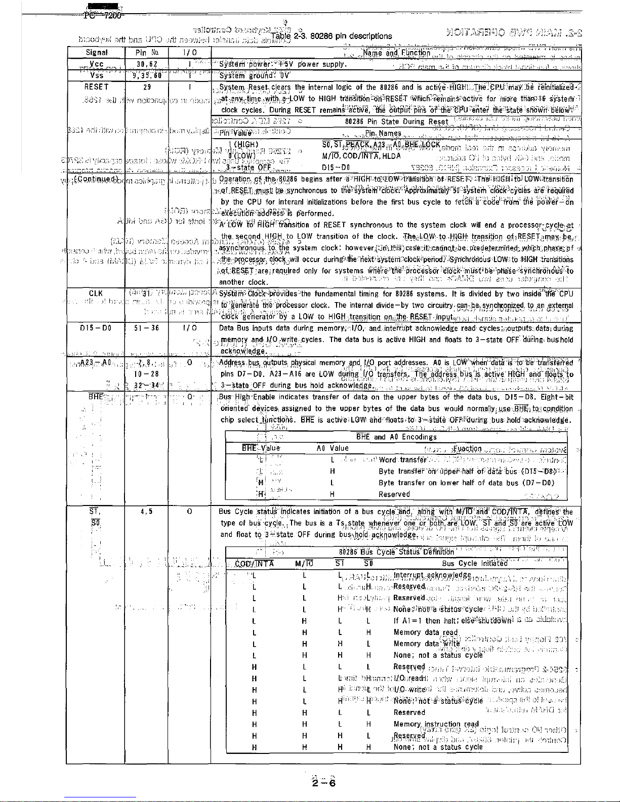
Signa!
Pin
No.
I/O
_---MJ.J1L-
0
CODIINTA
66
0
LOCK
68
0
READY
63
0
HOLD
64
I
HLDA
65
0
INTR
57
I
NMI
59
I
PEREQ
61
I
PEACK
6 0
BUSY
54
I
ERROR
53
I
CAP
51
I
-
PC-7200
Name
and
Function
M.eJn.Q.r.Y.::l1~_.dls.tiugujsh~
~mQ.a_--,!ccess
frolT!
1[0
~c9.es:s.
_If
HIGH.during
Is,
a memory cycle
or a halt/shutdown cycle
is
in
progress. If
LOW,
an
I/O cycle or
an
interrupt
acknowledge
cycle
is
in
progress.
M/TTI
floats
to
3-state
OFF
during bus hold acknowledge.
Code/Interrupt Acknowledge distinguishes instruction fetch cycles from memory data
read
cycles,
Also
distinguishes interrupt acknowledge cycles from I/O cycles. COD/INTA floats to
3-state
OFF
during
bus
hold
acknowledge. Its timing
is
the
same
as
M/iTI.
Bus
Lock
indicates that other system
bus
masters
are
not
to
gain
control of
the
system
bus
following
the
current bus cycle. The
LOCK
signal may
be
activated explicitly by the
·LOCK~
instruction
prefix
or automatically by
80286
hardware during memory
XCHG
instructions, interrupt acknowledge, or descriptor
table access.
LOCK
is
active
LOW
and floats
to
3-state
OFF
dUring bus hold
acknowledge.
Bus Ready
terminates a bus
cycle.
Bus
cycles
are
extended
without
limit
until
terminated
by
READY
LOW.
READY
is
an
active
LOW
synchronous input requiring setup and hold
times
relative
to
the
system
clock
be
met
for
correct
operation.
READY
is
ignored during bus hold
acknowledge.
Bus Hold Request
and
Hold Acknowledge cOntrol ownership
of
the
80286
local bus.
The
HOLD
input
allows another local bus master to request control
of
the
local bus.
When
control
is
granted, the
80286
will
float its
bus
drivers to
3-state
OFF
and
then activate
HLDA,
thus entering
the
bus
hold
acknoVlledge
condition.
The
local bus will remain granted to the requesting master until
HOLD
becomes inactive which
results
in
the
80286
deactivating
HLDA
and
regaining control
of
the local bus. This terminates the bus
hold
acknowledge condition.
HOLD
may
be
asynchronous to the system clock. These signals are active
HIGH.
Interrupt Request requests the
80286
to
suspend its current program execution and service a pending
external request.
Interrupt
requests are masked whenever the
interrupt
enable bit
in
the flag word
is
cleared.
When
the
80286
responds
to
an
interrupt
request,
it
performs
two
interrupt
acknowledge
bus cycles
to
read
an
8-bit
interrupt vector that identifies
the
source
of
the interrpt. To assure program
interruption,
INTR
must
remain active until the
first
interrupt acknowledge cycle
is
completed.
INTR
is
sampled
at
the beginning
of
each
processor cycle
and
must
be
active
HIGH
at
least
two
processor
cycles before the
current
instruction ends
in
order to
interrupt
before the
next
instruction.
INTR
is
level sensitive, active HIGH,
and
may
be
asynchronous
to
the
system
clock.
Non-
Maskable
Interrupt
Request interrupts the
80286
with
an
internally
SUPPlied
vector
value
of
2.
No
interrupt acknowledge cycles are performed. The interrupt enable bit
in
the
80286
flag word does
not
affect
this input. The NMI input
is
active HIGH,
may
be
asynchronous
to
the
system
clock, and
is
edge triggered after internal synchronization.
For
proper recognition, the input must have been previously
LOW
for
at
least four
system
clock cycles
and
remain
HIGH
for
at least four
system
clock cycles.
Processor Extension
Operand Request
and
Acknowledge extend
the
memory management
and
protection
capabilities
of
the
80286
to
processor extensions. The
PEREQ
input requests the
80286
to
perform
a
data operand transfer
for
a processor extension.
The
'PE7\'CK
output
signals the processor extension
when the requested operand
is
being transferred.
PEREQ
is
active HIGH and floats
to
3-state
OFF
during bus hold acknowledge.
PEACK
may
be
asynchronous
to
the
system
clock. PEACK is active
LOW.
Processor Extension Busy and Error indicate the operating condition
of
a processor extension
to
the
80286.
An
active
BUSY
input stops
80286
program execution
on
WAIT
and
Some
ESC
instructions until
BUSY becomes inactive
(HIGH),
The
80286
may
be
interrupted while waiting
for
BUSY
to
become
inactive.
An
active
E"R"RTIR
input causes the
80285
to
perform a processor
extension
interrupt
when
execution
WAIT or
SOme
ESC
instructions. These inputs are active
LOW
and may
be
asYnchronous
to
the system clock.
Substrate Filter Capacitor: a
0.041
,uF ± 20%
12V
capacitor must
be
connected
between
this pin
and
ground.
This
capacitor filters the output
of
the
internal substrate
bias
generator. A maximum
DC
leakage
current
of
1 uA
is
allowed through the capacitor.
For
correct operation of the
80286,
the
substrate
bias
generator must charge this capacitor
to
its operating
voltage.
The
capacitor chargeup time
is
5 m!lliseconds (maximum) after Vcc
and
CLK
reach their specified
AC
and
DC
parameters.
RESET
may
be
applied
to
prevent spurious
activity
by the
CPU
dUring this
time. After this time, the
80286
processOr clock
can
be
phase
synchronized to another clock by pulsing
RESET
LOW
synchronous
to
the system clock.
2-7
Page 14

~------=p~72a~~=·'----------~------------~----~------~----------~------------~
2·2.a; Clock
generator'(Fig.2·3,.,~-'n"
~'"
. ,,,'
:-Fi~~2,~~",s~9~s.
t:~e~~ir~(J;~9t.t.h!1:_-~PC-7?,Op
RI99,~-
g;~~~~~t?r;Jw~,i~[
,i~
- - .
'c~nt~n~d·,i~"t~~;~.q479t,t",_,,_,_
,._~.
,;,
... , -;-,:
.
-:i-,
-:
',,'\
Clock- 'ihpur-to·-the'
SC47Sf'
internal 82284 logic, 'is selected
to
.
.19.2MHz._J
6MHz~
or12MHz _
by
:tfie:'-s'jgnal
recei~ec'-.frodi'Jhe_CPU
i
016bl{,
select
'switch,'(S1)':
';A
:24~H_z:
clock"
is' ihterrially"diviaecFffito
:one,half.
,The)
'ciock,Jnput',isiinverted]i:1Side
the)82284-
to!
sl:.IjJprred'
1
)-_".'
as CPU clock, PROCLK, '
".
','
PROCLK
iodivided
;nto.'1/2,.1I4,01101716'
.by
theintafnal
frequency.
divid~r:to
bes~pplied
a~SYscU<'
PM;"CL~,
~nd.
SDCLK
. ,
,Sync,hr()nization
i,S,_atta'I,n,ed
with PROCLK:by the,signa!'
8_1'
~rom'
the_'
: CPU;' at' the firs't-'cycle- immedii3teiy
'after-_reset.
:
i=i~f
2-4
~h0WS
it~'
'timing~__
'J:"
,.
',.:i'·
, "
,(-,'
, 82284
LOGIC,
,
f---'--'+----'--'--l.
AI.
J
_,
.'
:,
I ,.1;
+2
_
A2
y
f----l
EFI
>-'0-1--
PROCu(
ose;:
§T
(from CPU)
DIVIDER
'-*2'
L'f---'r-1':=-.:....._t_.
SYSClK
SD,CLK
,DMA9,LK
Figure 2-3. Cleek generator circuit
PROCLK
,.
SYSCLK
SDCLK
c~~~
'FiQure'.2-4. Timing
~hai1
of
cibck circuit
,
J!
-,
",
:
-J.
:_"
-'
,,"
' , ,
~-2"4\;
Reset Circuit (Figures
~"5,
2"6'and~~7)
; Figure
2.,.5
'is'
,a-
block diagram
of:the~,reset
circuit,
'a:ncf
Figure, 2-6
show~,-,~
timing -chart
for_
this,
,circuit. There
a~e
two methods
in
resetting the computer:
-.
,--Sy~tem.-R'1~et",
.
);
:;"
,,:,
.,'
,
'.
I
This
r~set,i,s
p,erlormedbY,'fhe
,RES!:!
an-d
RES~Tsignals.
The
RE8E{kig~f,d
'is''6btaii1:~cfby
synchronizlng'this purse
sigmiJ
with
the system clock at the 82284 LOGIC. ' .
Oiimeotherhahd,-siriCe
the
'SC4751·erilitS·the CPU
HESEl'
"signal: atthe;-receptibrr-of the
RESET"signa~
';the--entire-system
- iocl!-jding
tJ;Je
_;C,PU
iSJ
reset., 1 '
,-
I
••
CP~
RE?s~t.
'J,),'
~.
J
,"
','
,
••
. This reset state is controlled
by
the CPU RESET siQnal. This
reset signal is emitted
when'a
CPU shutdown occurs,
or
when-the RC signal from the keyboard interface controller (8042) is
output.
The
shutdown state occurs when the CPU detects
an
internal error that prevents the execution of an instruction. If this
happens, the CPU denotes this state to the reset circuit making
the
SO
and
SI
signals LOW, MilO signal HIGH, and
AI
signal
LOW.
The RC signal is generated by the keyboard interface
controller on
the
CPU's order. This RC signal is used
in
the case
when the CPU changes
its operation mode from the protect
mode to the real mode.
-----
- Whefr-tne-CPV-is'
Fe~et,-iJ:first
tiegHJs
f'ft"
.execute1fjsfruC1iOffS
in
- ---
-~~t~~~~e,al
,modEl.:,~efore,
the-
q~u-
execuie~'lth'epbwer-O.O,
di,agnostic
."
progr~m:,
,it
re~dE/the
shutdown
st~tus
bYte
located
at
tile
addr~ss
. dFH
irithe
Ihlernal RAM of the RTC, Then tne CPU checks the
,:
reason~JQr:tbe':shlLtdbwn.
__
alld
__
Q~gilJs
_ procss_sing
__
13_cGQJ(Jjng:
to
-'"I
ttlei,irifOi'hiatioJi'written
in
the shutdown staius·
bYie.,
Tti&
CPU
i
~
RESET signgl;is':butput for the period
of
at
least 16 bus
cycli3s.
Fig.ure:;2:-,B.-s~ow~lthe
timing chart for the
CRU
reset.
------:-~-
52284
LOGIC
I
'",
"
..
,
, .
~ER
---f.-"---"--'~~--j
,
,(FROM
P~!
)-,-f-'-'
RESCf'U
SC4751
Fjg'ure 2-5.- Reset circuit
" .
_
~+~5~V~
__ --______
~~
+5V
':\:>_'---
GOOD
~
______
..J-----!!~_
..
POWER
POR
__________
-I----~!r!------,,_
(SYSTE
:~~i~~'
--"-'--~---~'-----!I~.--
RES
CPU
!~'h
Figure 2-6. Timing chart of reset circuit
CPU
RESET
S~U,T_
oo.WN
(SO·
$I.
AI_
0,
M/iO·
II
OR
RC(RC
-01
,,~Qyr~:?-7.
Timing chart of CPU reset
'1-,
~·~"5.
NMI.and
INTR
ContrOl Circuit (Figure
~·8)
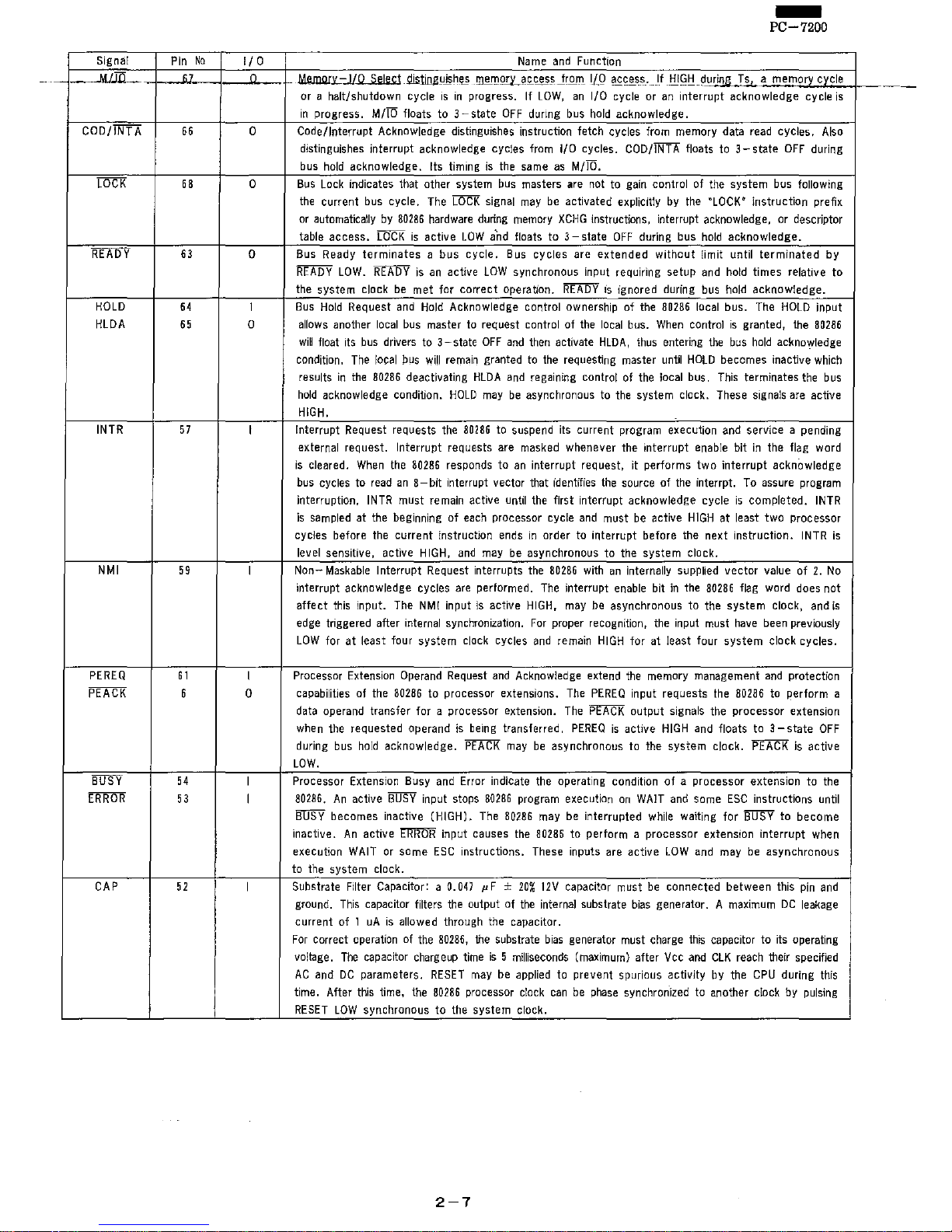
,The.-8,Q286"has nyo.'interrupt terminals; one is the Non-Maskable
Interrupt (NMI) and the other is tffeTnterri:.ipt. HOwever, in
tills
system,
the NMI signal is masked by ·the NMICS, ENAIOCK (Enable
110
Check) signals, (Refer to Figure 2-8.)
The
NMI terminal is used to detect a malfunction of
110
devices
connected to the optional slots.
CLRNMI signal is output from the 4-bit latch addressed at
061
H,
and the CS70H
Signal
addressed
at
070H is output from the
110
address decoding circuit
in
the SC4752.
The INTR signal is controlled
by
two PICs (PIC MASTER and PIC
SLAVE)
connected
in
cascade. The INT terminal
of
the PIC SLAVE
2-8
Page 15
-
PC-7200
is
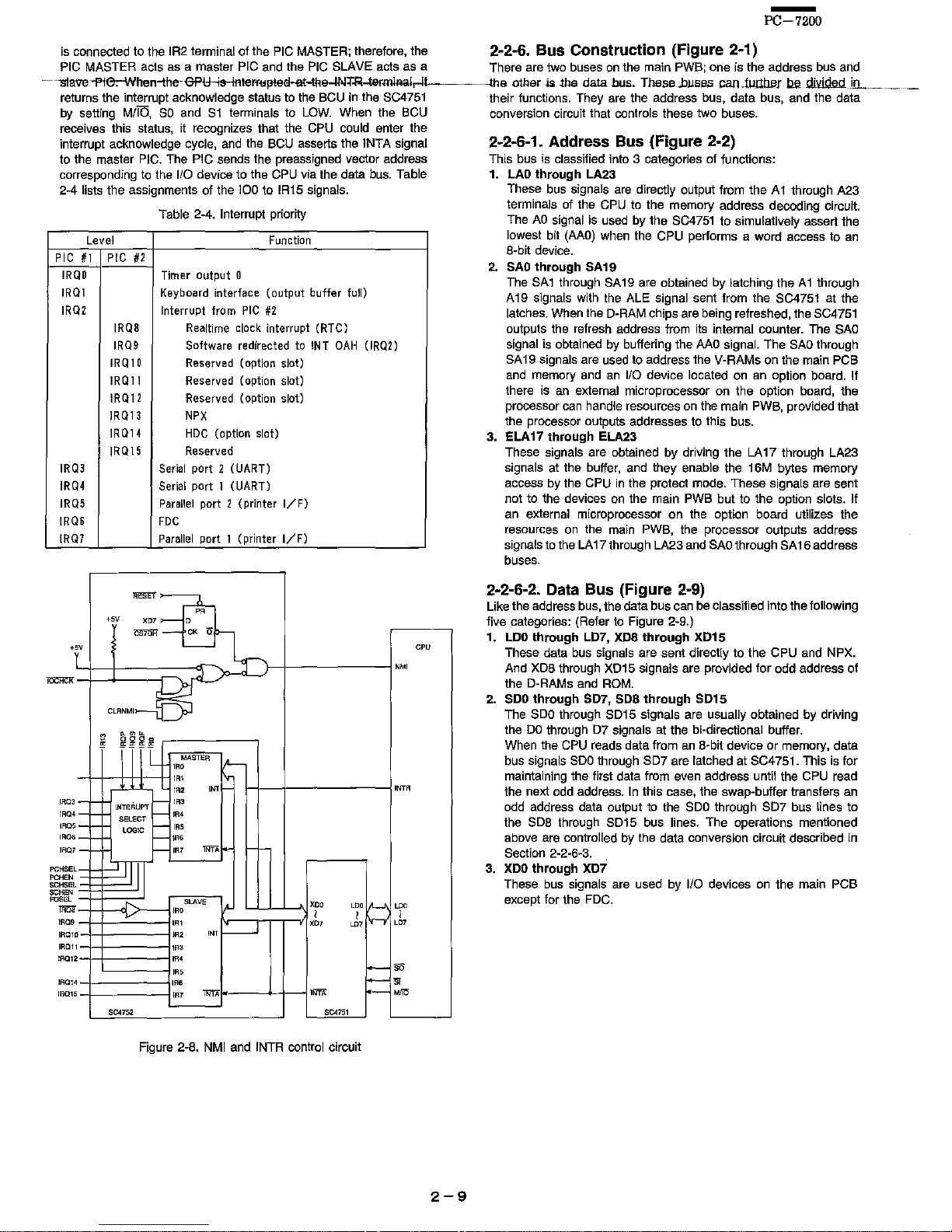
connected to the IR2 terminal of the PIC MASTER; therefore, the 2-2-6. Bus Construction (Figure 2-1)
PIC
MASTER acts as a master PIC
and
the
PIC
SLAVE acts
as
a There are two buses
on
the
main
PWB;
one
is
the address bus and
---slave1'te:-when-the-BP~-+.t-inteff~;>te<l
.... t-t"e-nlj:r.R-ter"'i"al,..ill-t
----tile
otio8f
is
the data bus. These.buses
canJulllleJ
bl1.
dil'i.del!h..-
__
_
returns the interrupt acknowledge status
to
the BCU
in
the SC4751 their functions. They are the address bus, data bus, and the data
by setting
MiiO,
SO
and
81
terminals
to
LOW.
When the
BCU
conversion circuit that controls these two buses.
receives this status,
it
recognizes that the CPU
CQuid
enter the
interrupt acknowledge cycle, and the BCU asserts the
INTA signal
to the master
PIC. The PIC sends the preassigned vector address
corresponding
to
the
110
device to the
CPU
via the data bus. Table
2-4
lists the assignments of the 100 to IR15 signals.
Table 2-4.
Interrupt priority
Level
Function
PIC
#1
IRQO
IRQ
I
IRQ2
IRQ3
IRQ4
IRQ5
IRQ6
IRQ)
f
,-
.-
,-
;-
,-
,-
PCHSE
PCHEN
SCHSE
SCHEN
FOSEL
,
-
tRa9
"
"
'"''
IRal
,
•
,
PIC
#2
Timer
output 0
Keyboard
interface (output buffer full)
Interrupt from
PIC
#2
IRQB
Realtime
clock
interrupt
(RTC)
IRQ9
Software
redirected
to
IN T OAH
(lRQ2
)
IRQ
I 0
Reserved
(option slot)
IRQII
Reserved
(option slot)
IRQI2
Reserved
(option slot)
IRQI3
NPX
IRQI4
HDC
(option slot)
IRQI5
Reserved
Serial
port 2 (UART)
Serial
port 1 (UART)
Parallel
port 2 (printer
I/F)
FDC
Parallel
port 1 (printer
I/F)
""'"
"
..
,
'"
0
""""
"
"
'M'
C~'M'~
~
tnt
MASTER
I-
'"'
,-I--U--
'"
'"
,m
''''"
INTERUPT
~
'"
SELECT
'"
LOGtC
~
'"
'"'
r--
tR7
'""
~
SLAve
'"
""
c:::;
'"
-
'"
,
,
,
'"'
~
'"
cm
co,
'"'
'"'
'"'
'"
'"
-
""
'"'
~
,.
'"
'"'"
-
"""
5C4752 504751
Figure 2-8.
NMI
and
INTR control circuit
C'"
2-9
2-2-6-1. Address Bus (Figure 2-2)
This bus
is
classified into 3 categories of functions:
1.
LAO
through
LA23
These bus signals are directly output from the
A1
through A23
terminals of the
CPU
to
the memory address decoding circuit.
The
AD
signal
is
used by the
SC4751
to simulatively assert the
lowest bit
(AAO)
when the CPU performs a word access to
an
8-bit device.
2.
SAO
through
SA
19
The
SA1
through SA19 are obtained by latching the
A1
through
A 19 signals with the ALE
Signal sent from the SC4751 at the
latches. When the
O-RAM chips are being refreshed, the SC4751
outputs the refresh address from its internal counter. The
SAO
signal
is
obtained by buffering the
MO
signal. The
SAO
through
SA 19 Signals are used to address the V-RAMs on the main PCB
and
memory
and
an
1/0
device located on an option board. If
there
is
an
external microprocessor on the option board, the
processor
can
handle resources on the main PWB, provided that
the processor outputs addresses
to
this bus.
3.
ELA
17
through
ELA23
These signals are obtained by driving the
LA
17 through LA23
signals at the buffer,
and
they enable the 16M bytes memory
access by the CPU
in
the protect mode. These signals are sent
not to the devices
on
the main PWB but to the option slots. If
an external microprocessor on the option board utilizes the
resources
on
the main PWB, the processor outputs address
signals
to
the
LA
17 through LA23 and
SAO
through SA 16 address
buses.
2-2-6-2. Data Bus (Figure
2-9)
Like the address bus, the data bus can be classified into the following
five categories: (Refer
to
Figure 2-9.)
1.
LOD
through
L07,
XOS
through
X015
These data bus signals are sent directly
to
the CPU and NPX.
And
XOB
through XD15 signals are provided for odd address of
the D-RAMs and
ROM.
2.
SOD
through
S07,
SOS
through
SOlS
The
SDO
through
8015
signals are usually obtained by driving
the
DO
through
07
signals at the bi-directional buffer.
When the CPU reads data from
an
8-bit device
or
memory, data
bus signals
SOO
through
S07
are latched at SC4751. This is for
maintaining the first data from even address
until the CPU read
the next odd address.
In
this case, the swap-buffer transfers an
odd
address data output
to
the
SOO
through
S07
bus lines to
the
SOB
through S015 bus lines. The operations mentioned
above are controlled by the data conversion circuit described
in
Section 2-2-6-3.
3.
XOD
through
X07
These bus signals are used by
1/0
devices on the main PCB
except for the
FOC.
Page 16
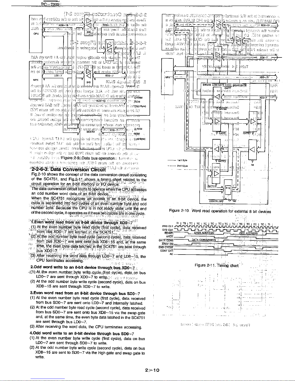
;
,:;';-;,:-:
8,);1,\
,IYOJriJ.
';": 1 f
ni.
'rJ
'oJ13
,~:~ifk)
;\:1:;;·-:
:j
';r!j nxP?
.;';:Jr!'(;lRAM
~"
'"h'''''
- -
"-'i".~~)~,
_'~"~'~"'_'_'~"X70~'_:""~"'-',i!~'~"_"\_'_-~"~"'v'li'
-0;'
'-:ROM
J"i:ii.;'_)1rij
Qr\8 :-l;;T
..
ii;'~:;
04;'\
-")fi!
:,:;r·!j);-,~;:r:
\('-~
l),o.l'i!;,t;-ic,i
~!
1,;jr(tl,ighByte)
r\Y1
n::;ill
_J;1l
:1')
-3.
'/],- ,;! ,\,I
;-)rii
"~d:-rJ;,)b:-'i
'J:
j~)GU
,Ii:-,
,-"i;~:
l~J'~
'-'
i ,
II
'}b
:{l
nniU;"
fir
nJ
:n-,"--;:c':;~
~;'::::'::::';
':>1
.'F'
jnt:;
'nol:"h'0~'~
.
...,.""--
";
':,
~:~~:~;
;~~~,:;~,:;.~
~o~~~;~;;~:,I,'.;:,;;,·;:;,~~£:'.
::);~~iM
;:,., ,
__
' .';")
;-~_;'iIJ~
)-!~
R~M
.:'
','i)~
,
r,
,!j':.ji' ,viJ iiJd
FJ';-.r'.
ni.s,-,i
::Jf:;-
'-IQ
_:::'!:Jl'd;_'
!,l,
,',-):;;:I;:J
'.
i
,CO)
lFigt.irE!'2-g-~JD.ata
-bus
Dp-er~tioh,;
L'
' -r)
'!lpV>'Byte)
~}-'-i~!;:";
,~;I',V
,-.,,,
'j:>}:-'-1
::-i:
-','J;
iljc,fTl
,:"it
'1--:'
c!-)-j:')
r")
~Z-2l6
..
3i/'D~f~
'e:b:nV~'rsidH~circuit'~;:U
'j
II))
-'[-;;-'1,""
Fig,2-10 shows the concept of the data conversion circuit'c6ris-iSling
of the SC4751, and Fig,2
i
1)1,{,shQ~~_
~:t~ll]ipg~~,ph'?rt.rela!_~ct
tQ
_.t~e
circuit 0 eration for an
8-llif
manic
·.J'--~rJliO"device:--'
_'J,
.~.
'I..'
-'"
--,
'.lT~~J~~t~hbriljJt~f6~~gi~b~urtiM~_rt~:t6·%p~r~te
~h~~lthe
C?ti
d6~e's~-es
an
odd number word
~,a,t~,of,:~.~~,g~~ir'~~~jce_:~"l
;:
i
-~:,),~:;~"':~'1
1 )
:';,'
"Yt1~9"
th~
·l?P~?~1
.
r~fqg,~f~e:~:~h·.~a_~c"e~$s
J]
~r:i;8~pjt:-d,~viq~,
the
~~I~;;i,~,
~ep¥~~edS~t9"_
t,~f)~r~~Ef~
,dJ~~~;'~v.11.n~n~~-njg:~'r:p~~,~np
odd
rllimb'ei(byte~
B~da(i~je
-tiie-
CPU'
i~:
in'
i'-dr
re,ady'
stat¢:'u:ritil
the
end
of the second cycle, it
operq!e§,a~,if,m~~,e_two,~~c)~(W~'
j~-O~,e:I!¢YCI~.
~'-.J~,),
"_"JI
__ ' ",,-,
'~".I
.. , ..
,,,)11..
",L~,
•
;
)'1IJ~{,~nci"J~Ic(r~;ad"trdrrtJa';
!;a-bli
id~vit:Erih~b~;~w
3d3ojt
'i1
i
(1) At
th~
'e~~ri
'riuRurer
ii
bY,i1
:r~kiF
.:.!6ie:;(first
h
~I~r,~'~lafa-:
r~c
..
i~ived
'~','
'f'r_-r']
'-~~"'~"""I"'-'-)---
,-,-,,9Y.,,\
,---,,,y'YJ'--
'~"-"'I'
.
d~_"
JrtJiifbus.
XOtr..:.::t-aJ~'
ia~cn~djii
tHs'-SC475L,.''-',
11,) , ,-"
.i:(2r:11(t)'ri~
,~~~~~{,mb~t~~~
~~~~:
f~~j~
~(~~q8.~:6Y,t,~~~'~~at~i~beived
"
',-,
"from' bus
"XOO":';'Tare
:sent'
onto
b(]s"JSOe~15"an'd~",atJthe
same
,1:;
"tTIfle-/'t"n~
~Q&i1i~§iErdiii~JMCfMd%
tf,lSC4151-are,'se'nt throu h
::,t
,·~tGs:xb6\:;.;7.
:'h":)-:.-,:?,,:-,,
-~r,)
:);}
;".!i~~~'
:"::'
"';:~1;~':
':,
';j;~
9
:.~3)
An_~'~
11re)-t,~WI.~-gOjK~~fterd,;~~t~
JW~~~~,h'
(0,
b~i
_~'~·~~~D~;-j~,
the
."
CPU
erminate::d:lccessin'g:"'"
.-'
"',
'''-'--, ..
, ,,'
.,
.
,:~
-i ~ - 1,
-J
i)'
, ;
2.0dd
word write
to
an a-bit device
throl,lg~
l;nt~)'Xp,O,",,!?:
-j(HAUhe
,,?,,,en
,nu!T:!I;l,!9Lbyt~
write"~gy;cle:,-(fiE§t:
~YGfe);_
!=I~ta,;,on
bus
LOO-7
are
sent through XOO-7
to
writ~;j'
,,":)
1
~-)
J'_i''-}-r.',-,
(2) At the odd number byte write cycle (second cycle), data
on
bus
X08-15
are
sent through XOO-7 to write.
3.Even word read from an a-bit device through
bus
SOO-7
(1)
At the even number byte read cycle (first cycle), data received
from bus
SOO-7
are sent onto LDO-7 and internally latched.
(2)
At
the odd number byte read cycle (second cycle), data received
from bus
SOO-7
are sent onto bus
X08-15
via the swap gate
and,
at the same time, the even byte data latched in the
SC4751
are sent through bus LOO-
7.
(3) After receiving the word data, the CPU terminates accessing.
4.0dd
word write
to
an a-bit device through bus
SOO-7
(1)
At
the even number byte write cycle (first cycle), data
on
bus
LDO-7
are sent through SOO-7 to write.
(2) At the
odd
number byte write cycle (second cycle), data
on
bus
X08-1S
are sent to SOO-7 via the high gate and swap gate to
write.
1
;\),11
::
j,
\()
T
iii
1
1
Iii
II:
II~
--
1s118yte
----
2nd 18Vle
CONTRLOFF v-'-AO
Figure
2-10. Word read
~peration
for'
e~erlial
8 bit
devi~es
PRO
ClK
TI I TS I TC I TC
I
T<f
I TC J
TC I TC
I TC 1 TC
-(
TC J TC ! TC
Ii
TI
I
SYSClK
I _
,_
~
iIDiWR:----.
EVEN ADDRESS! r--:-"J
~
___
ODD
ADDRESS
I
r--
ARDY
-----.I
DATA
CON\(--'
ARDlf
EN:~
END
CYCLE'
CONTOFfi
AO
,~
DATA CONY:ERSION:
"I
I
-~
--
__ : __
,
r--
Lf..J;
L...--l
--
'--,
~i
2>10
Page 17
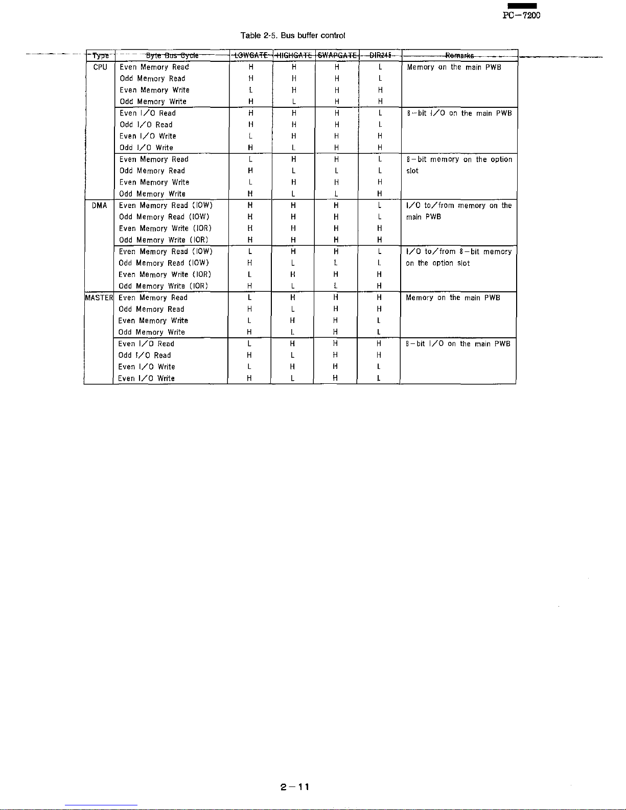
-~-.
-Byte-Bos-flyeIe
--
CPU
Even
Memory
Read
Odd
Memory
Read
Even
Memory
Write
Odd
Memory Write
Even
I/O
Read
Odd
I/O
Read
Even
I/O
Write
Odd
I/O
Write
Even
Memory
Read
Odd
Memory
Read
Even
Memory
Write
Odd
Memory
Write
DMA
Even
Memory
Read
(lOW)
Odd
Memory
Read
(lOW)
Even
Memory
Write (JOR)
Odd
Memory
Write (lOR)
Even
Memory
Read
(lOW)
Odd
Memory
Read
(lOW)
Even Memory Write (JOR)
Odd
Memory
Write (lOR)
MASTER
Even
Memory
Read
Odd
Memory
Read
Even Memory Write
Odd
Memory
Write
Even
I/O
Read
Odd
VO
Read
Even
I/O
Write
Even
I/O
Write
Table
2~5.
Bus buffer control
-i."W&I,-E-
-HIGH&I,-E-
-6WA~".f
H H
H
H H H
L
H H
H
L
H
H
H H
H H H
L H H
H
L
H
L H H
H
L L
L
H H
H
L L
H H H
H
H H
H H H
H H H
L
H
H
H L
L
L
H
H
H L L
L
H
H
H
L
H
L H H
H
L
H
L H
H
H
L H
L
H
H
H
L
H
2
-11
--IlIR.1-1i--
L
L
H
H
L
L
H
H
L
L
H
H
L
L
H
H
L
L
H
H
H
H
L
L
H
H
L
L
Remar-k-s----
Memory
on
the
main
PWB
-
PC-7200
B - bit
j/O
on
the
main
PWB
B bit
memory
on the option
slot
I/O
to/from
memory
on
the
main
PWB
I/O
to/from
8-bit
memory
on
the
option slot
Memory
on the main
PWB
B - bit
I/O
on
the main
PWB
Page 18
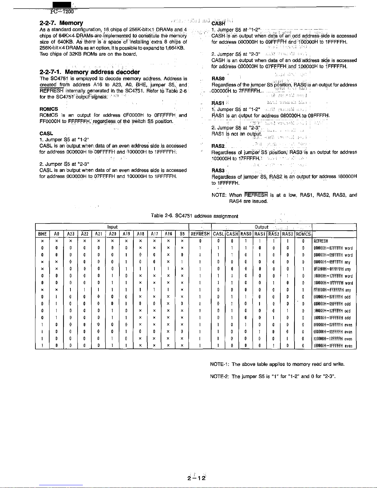
-',
-PC~"7200
'"
2-2-7. Memory
As a standard
configuratiqn-!-
16,-chips
of 256KMbitx.1--.DRAMs
and.-4
chips
of
64K-x.4--CMMs-are-'jhlfJle
rTl
ented
td
constitute the
memory
size of 640KB. AS'there 'js'a-
space'o~\listalling'extra
8 chips of
256K-bitx4 DRAMs
as
an
option,
it
is
possible
to
expand
to
1,664KB.
Two
chips
of
32KB ROMs are
on
the board.
2-2-7-1. Memory address decoder
is
employed to decode memory
ad~ress.
Address is
address A16
10
A23,
AD,
SHE, jumper S5, and
i'nternaIlY
__
generated
in.
the SC4751. Refer
t6.
Tabf~
2M6
for the SC475FouipufsignalS. '1,-,1
.j
ROMCS
ROMCS
is an output for address
OFOOOOH
Iq
OFRFFFH
and
FFOOOOH
10
FFfFFFH:rel!,jf~le~s,
bphel
'swilen
55
POsilion,
CASL
1.
Jumper
55
al
"1-2"
CASL
is
an
QulpJJ1JI'Lhen_data.
oj
an
_even
address sjde
J~
aca8'ssed
for address
OOODODH
tb09FFFFH
andlOOOOOH to 1FFFFFH;
2.
Jumper
~5
al
"2-3"
CASL
is an 'output when data of
an
even address side is accessed
for address
OOOOOOH
10
07FFFFH and 100000H to 1 FFFFFH.
",J
CASH"
1~
J_umper
85
at-'!1--2!':,-
_
:'11
'
.",~.-.-;-
------:-
~_'~-,
CASM'ls:an-output
when:
data-'of
an"
odd adqress-side
is
accessed
for address
OOOOOOH
10
09FFFFH
~~dlbdiJoOH'IO
1FFFFFH.
"
'J
2.
Jumper S5 at "2-3"
.;,
,
CASH
,is
an
output when
data
of
an·
odd
'address
side
is accessed
fqr aaqress
OOOOOOHto
07FfF'fHano,iOO,OOOH to
iFFFFFH.
RASO
",
Regardi,ess
of the jumper
85
j~J~itio'n,
'RASQ-
is
an
output for address
-0000001'1-10
7FFFFFM.__
""'.""
','
c·,,,
..
RAS1':
'''''';
"" , ..
""
..
1l
Jumper
85
at "1-2"
),
:'.;/
-'u
'-J'"i
~AS1
is an Qulput for address
o.aQOQQH,
IQ
09FFFFH.
I
;'/,
) I '
-,
~
2,.
Jumper S5 at "2-3" ,
..
,
RAS1
is
not
an
out~_yt.
,
"'i
Regardiess
Clf
jum'periSS'positioh,;
RAS3"I!:;
an output for address
100000H to 17FFFFH.'
RAS3
Regardless of jumper
S5~
RAS2 is an
outputfor
~ddres5
180000H
to 1 FFFFFH.
,'
...
NOTE: When REFRESH is at a low, RAS1, RAS2, RAS3, and
RAS4 are issued.
Table 2M6.
SC4751 address assignment
Input
Output
BHE
AO
A2l
A22
A2l
1120
AI9
A18
All
A16
S5
REFRESH
CASl
CASH
RASO
RASl
RAS2
RASl
ROMCS
x
x x x x x
x
x x x x
0
0
0
1
1 1 1
0
REFRESH
0
0 0 0 0 0 0
x
x
x x
1 1 1 1 0
0
0
0
OOOOOOH
....
07fFFFH
word
0
0
0 0
0 0
1
0 0
x
0
1
1
1
0
1 0 0 0
080000H-09FFFFH
word
x
x
0 0
0
0 1
0
0
x
1 1 0 0 0 0
0
0
0
080000H-09FFFFH
any
x
x
0 0 0 0
1
I 1
1
x
I
0
0
0
0 0 0
1
OFOOOOH-OFFFFFH
any
0 0 0 0
0
1
0
x x x x
1 1 1
0
0
0
1
0
IOOOOOH-17FFFFH
word
0
0 0 0 0
1 1
x
x
x
x
1
1
1
0 0
1 0 0
180000H-1
FFFFFH
word
x
x
1
1
1
1 1
1 1 1
x
1
0
0 0 0
0
0
1
FFOOOOH-FFFFFFH
any
0
1 0 0
0
0 0
x
x
x
x
1 0 1 1
0 0
0
0
OOOOOOH-07FFFFH
odd
0
1
0 0
0 0
1
0 0
x
0
1 0 1
0
1
0
0 0
080000H-09FFFFH
odd
0 I 0 0 0 1 0
x
x
x
x
1 0 1 0 0
0
1
0
JOOOOOH-17FFFFH
odd
0
1 0
0
0 1
1
x x
x
x
I
0
1
0
0
1 0
0
180000H-IFFFFFH
odd
1 0 0 0
'0
0 0
x
x
x x
I 1 0 1 0
0
0
0
OOOOOOH-07FFFFH
even
1
0 0
0
0 0 1 0 0
x
0
1
1
0
0
1 0 0 0
OSCOOOH-09FFFFH
even
1 0 0 0
0
1 0
x x x x
1 1 0 0 0
0
1
0
lOOOOOH
....
17FFFFH
even
1
0 0 0 0 1 1
x x
x
x
I
1
0
0
0 1 0 0
180000H
....
1FfFFFH
even
NOTE~
1: The above table applies to memory read and write.
NOTE-2: The jumper S5 is
"1"
for
"1-2" and 0 for "2-3".
Page 19
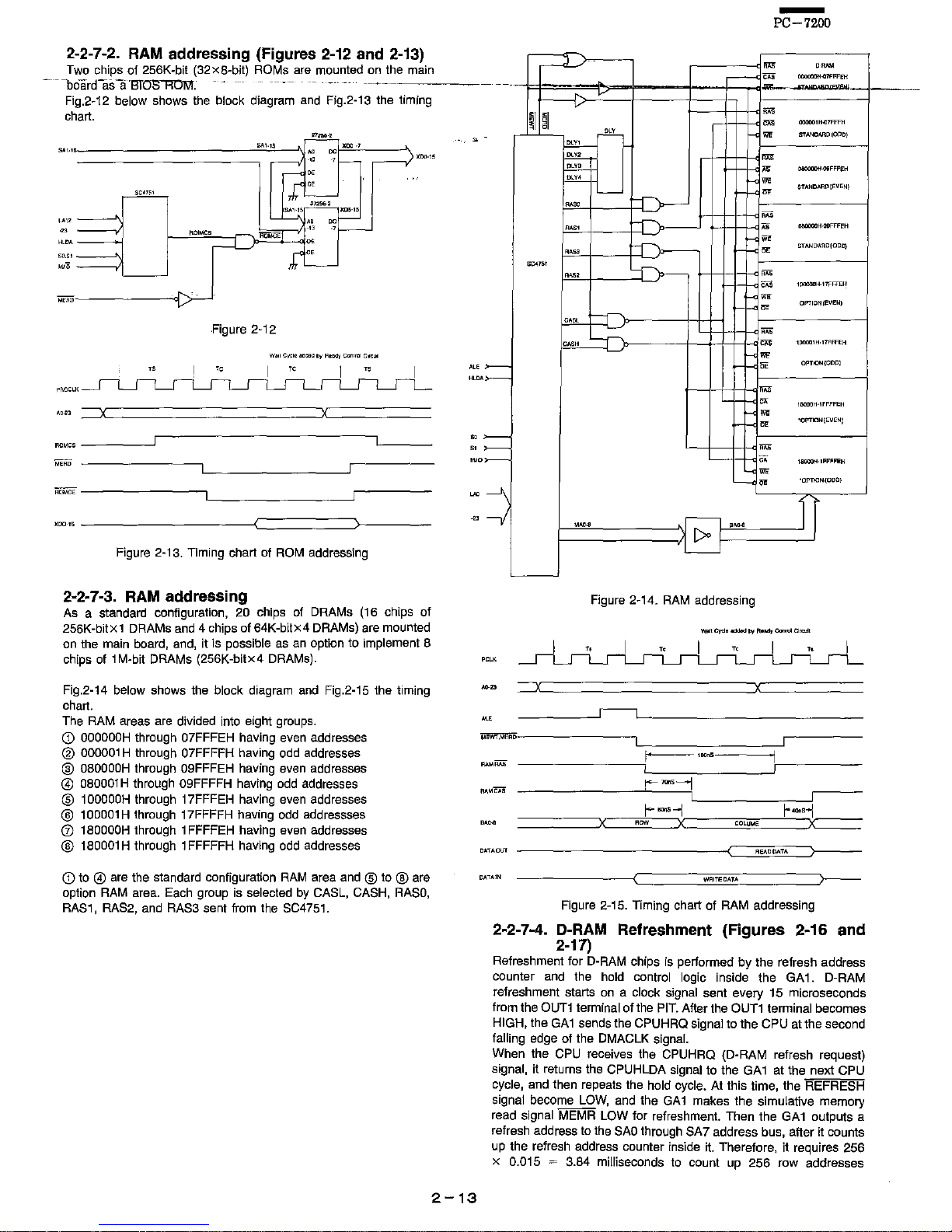
2-2-7-2. RAM addressing (Figures 2-12 and
2-13)
Two chips of 256K-bit (32xB-bit) ROMs are mounted on the main
-
-boardas a ·8TOBtmM.
-----
Fig.2-12 below shows the block diagram and Fig.2-13 the timing
chart.
S~'.'5::===========~~~'·'5=:j.
oo,W·"oo".,
__
--'\
.,~
7 XDo·,5
H'OA
__
~
SO,S!
MilO
SC"5'
1l0lMCS
Figure 2-12
Ao,~l
:=:::X=============::JxC======
ROMes
____
J-------------,
__
_
•
--
,:=
:=
-
V
!iii
~
~
I 1Jl1'2
I
OLYl
~
L-
AA.
~,
..
"
SC41~t
"~,
~
""
CASH
L;--,
-
PC-7200
"'"
"~
,-----<
""
OO,.,ODIHI7FFFEH
~---aT~
""
""
OODOO1H.cl7FFFH
'"
STANCI.RDIODD)
'"
"
tJBOOOO1H'IIFFFEH
..
"
STANDARD
(EVEN)
:::fJ,----
I=:rJ,-
"~
~
IlIiOQQOH.oIIFFfEH
f--n,-
'"
1-<'"
STAND~AD(ODIll
~
"~
"~
HIOOOOH·I7fFFEll
""
'"
OPTION
(EVEN)
"~
'"
HIOOIl1H·17FFHH
"'
'"
OI'TKlNIDODI
'"
ox
ISODOH·'FFFFEH
'"
'"
"O!'TION(EVENI
"~
"'"
,~
"
I8ODOH·'FFFFEH
~--------L_
________
-'----
'00"'
_________
---<=====::>--
___
_
Figure 2-13. Timing chart of ROM addressing
2-2-7-3. RAM addressing
As
a standard configuration,
20
chips
of
DRAMs
(16
chips of
256K-bitX1 DRAMs and 4 chips
of
64K-bitx4
DRAMs) are mounted
on the main board, and,
it is possible as an option to implement 8
chips of 1
M·bit DRAMs
(256K-bitx4
DRAMs).
Fig.2-14 below shows the block diagram and Fig.2-15 the timing
chart.
The RAM areas are divided into eight groups.
CD
OOQOOOH
through 07FFFEH having even addresses
® 000001 H through 07FFFFH having odd addresses
®
OeOODOH
through 09FFFEH having even addresses
@ 080001 H through 09FFFFH having odd addresses
®
10DaOOH
through 17FFFEH having even addresses
® 100001H through 17FFFFH having odd addressses
o 180000H through 1 FFFFEH having even addresses
® 180001 H through 1 FFFFFH having odd addresses
CD
to @ are the standard configuration RAM area and ® to ® are
option
RAM area. Each group is selected by CASL, CASH, RASa,
RAS1, RAS2, and RAS3 sent from the SC4751.
.•
2-13
..
,---<"
'OPT~N(OOO)
---\
1
-I
•••
,~
I>
Figure 2-14. RAM addressing
~.
~~==============~x~=======
________
,--,L
____________________
__
-=~~~
I
,oonS
R,OJ,IfL',S I
r-
7OnS--j
r-~--I
=====X
ROW
X
CATAOIJT
_____________
--(=:::;""~~"""~;;;:"=:::>_---
DATAIN
WI1ITEOATA
>---
Figure 2-15. Timing chart
of
RAM addressing
2-2-7-4. D-RAM Refreshment (Figures 2-16 and
2-17)
Refreshment for D-RAM chips is performed
by
the
refresh address
counter and the
hold control logic inside
the
GA1. D-RAM
refreshment starts on a
clock signal sent every
15
microseconds
from
the
OUT1 terminal
of
the PIT. After the OUT1 terminal becomes
HIGH, the
GA1
sends the CPUHRQ signal to
the
CPU
at
the second
falling edge
of
the DMACLK signal.
When the CPU receives the CPUHRQ (D-RAM refresh request)
signal, it returns the CPUHLDA signal to
the
GA 1 at
the next CPU
cycle,
and then repeats the hold cycle.
At
this time, the REFRESH
signal
become LOW, and
the
GA 1 makes
the
simulative memory
read
signal MEMR LOW for refreshment. Then
the
GA1 outputs a
refresh address to the
SAO
through
SA7
address bus, after it counts
up
the
refresh address counter inside it. Therefore,
it
requires 256
x
0.015 = 3.84 milliseconds to count up
256
row addresses
Page 20
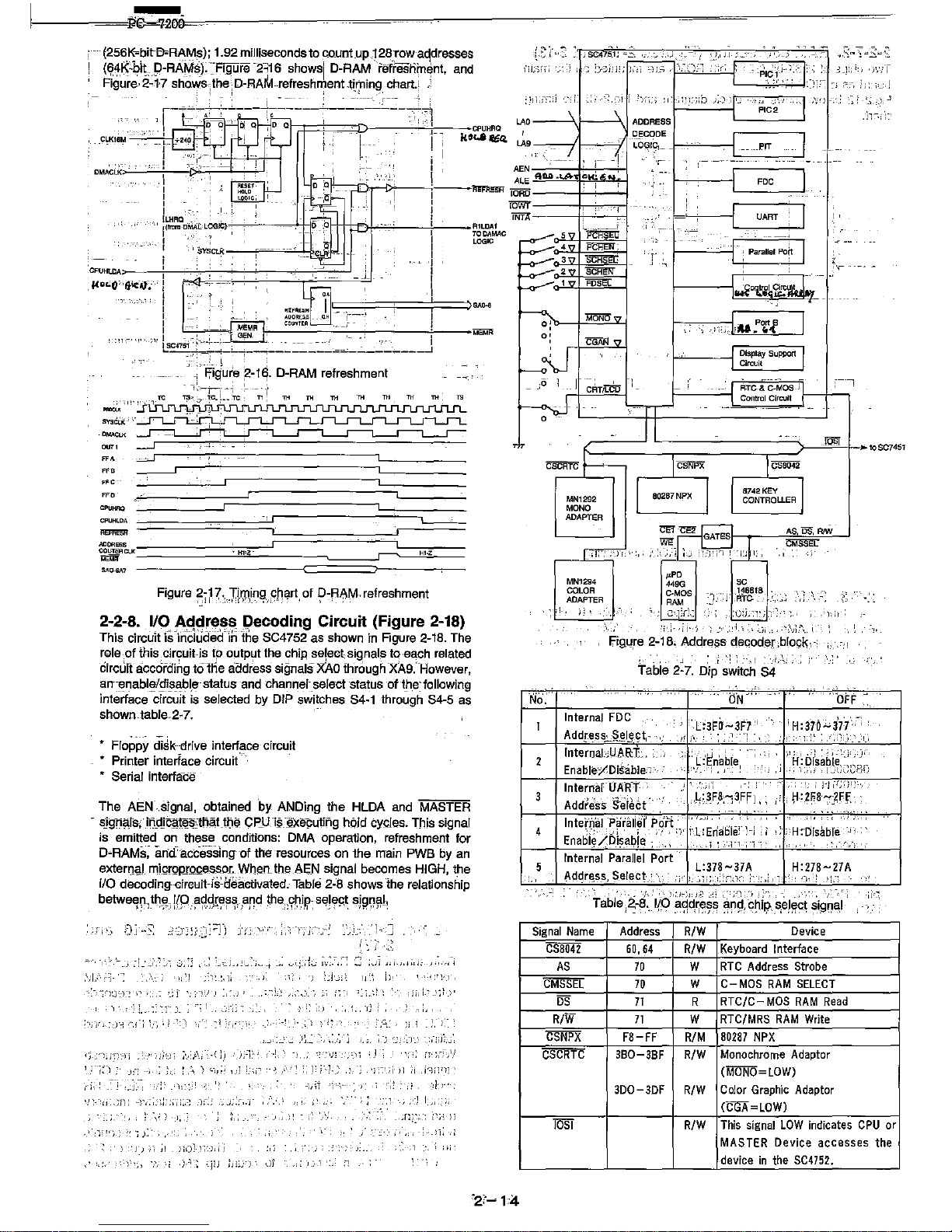
.
(256K-..bit-Er-RAMs);
1.92
milliseconds
to
cQunt
up J 28-row
addresses
(~4K~bit
p-RAM,rFlgure2"16
showsi
D-RAMfef;estiin~n1,
and
Figure,2-17
shaws_]the;
D-RAM--refresh~ent<ttrping,
chart)
.1
'CF'UHlCA
,1'°'-0
'fiiC-v~
-
sYsco."··
·co
,-,·r-"Lrll
,,-
••
,r-U"""L--,",-r,--,,
''-_'"L
•
DMACLK
~,
~<
~,
~,
~,
CPUHRQ
-I,
Figure
2-17.
Timing
chart
of
D-RAM.refreshment
:,i
,.:",,)\'.1.,
,'j,,-"':"
,',
2-2-8_
1/0 Address Decoding Circuit (Figure 2-18)
This
circUIt
is"j'nclJded'lr,
'the
8C4752
as
shown
in
Rgure
2-18.
The
role-,of
this
circuit-·is
tp
outp~t
the
chi~
_
select
si~nal$
to
·ei;l,ch
related
Circuit
a:ccofdi~g
to
Uie
a:adress
signals
XAO
fhrougn
XA9.'However,
an~enable/disable'
status
and
channel-
select
status
of
t_he~following
interlace
-arcult
is
selected
by
DIP
switches
84-1
through
84-5
as
shown_table.2~7.
.
Floppy
di~k--drive
interlace-
circuit
Printer
inteMace
circuit'
Serial
interlace
The AEN.signal,
ob1ained
'by
ANDing
1he
HLDA
and
MASTER
-
sjgi1~ls.'ii').Qic:at_i;i~';tn~tJlje
C~U-i~_'~xeputillg
hqld
cycles.
This
signal
is
emitted
on
these
conditions:
DMA
operation,
refreshment
for
D-RAMs;
~md'
accessln~r-of
the
resources
on
the
main
PWB
by
an
extenw,J
miQrQP_JQ~e$SPI,
When_the
AE;N
signal
becomes
HIGH,
the
I/O
decoding--circuit-ts~deactivated.
Tablei
2-8
shows
the
relationship
betwe~~t~~_lVP;~Rgr~~~:jand
the;H:f:1,jJ?;s~lr~
sjQ~~h
,J,
.•
,'.
,,;~,
1_
--j
~. ~'
__
j.
L..-
'',.'.'
;,-1
,""
",',
'"
"I,;"
'.;]
,:.,"'):'
:
,~
-;
~1,:'
",.
:;)~
J'
)
i-I
,1
;,
IIJ1-
)~'
J, i ;
~j'j;'
II
'j
lJ,·
1
,,/:t).
J '
,,'
~)
..
I"
j·~l.)
;,;.j
'.
,"
:'j!
j
;,-)
I
,r:~>
-.
"
II
iii·
'-'.'"
i-·l;
'I!)
II
Eo")·,
di
,:; J "
','
:]
4
r
:r~~:'~'"'"~'"'~
:o_F
i"
,)';,
;>-.1,
',>j
,i " :.'
MN1292
MONO
ADAPTER
MN1294
COLOR
ADAPTER
i!
Internal
FDC
ON
,':.L.
'.,.3F"a.~._
.•
3,F7,.
,.',
Add[ess.:..~~I_~~t,.
" '.
'--,
,-
;"t,r;;)I;'
'I
W2F,B,72Ff
.,
Internal
Parallel
Port'
L:m
-37
A _
......
H. : ..
2,.7."B -..
".2
... 7 A.
.
Addre,s.s,
Select,·· :
:f~'Y:
: 1:,,)
Signal
Name
Address
R/W
Device
CSB042
60,64
R/W
Keyboard
Interface
AS
70
W
RTC
Address
Strobe
CMSSEL
70
W C
MOS
RAM
SELECT
OS
71
R
RTC/C
MOS
RAM
Read
R/W
71
W
RTC/MRS
RAM
W,i1e
CSNPX
FB-FF
R/M
B02B7
NPX
CSCRTC
JBO-JBF
R/W
Monochrome
Adaptor
(MONO~LOW)
JOO-30F
R/W
Color
Graphic
Adaptor
(CllA~LOW)
10SI
R/W
This
signal
lOW
indicates
CPU
or
MASTER
Device
accesses
1he
device
in
the
SC4752.
Page 21
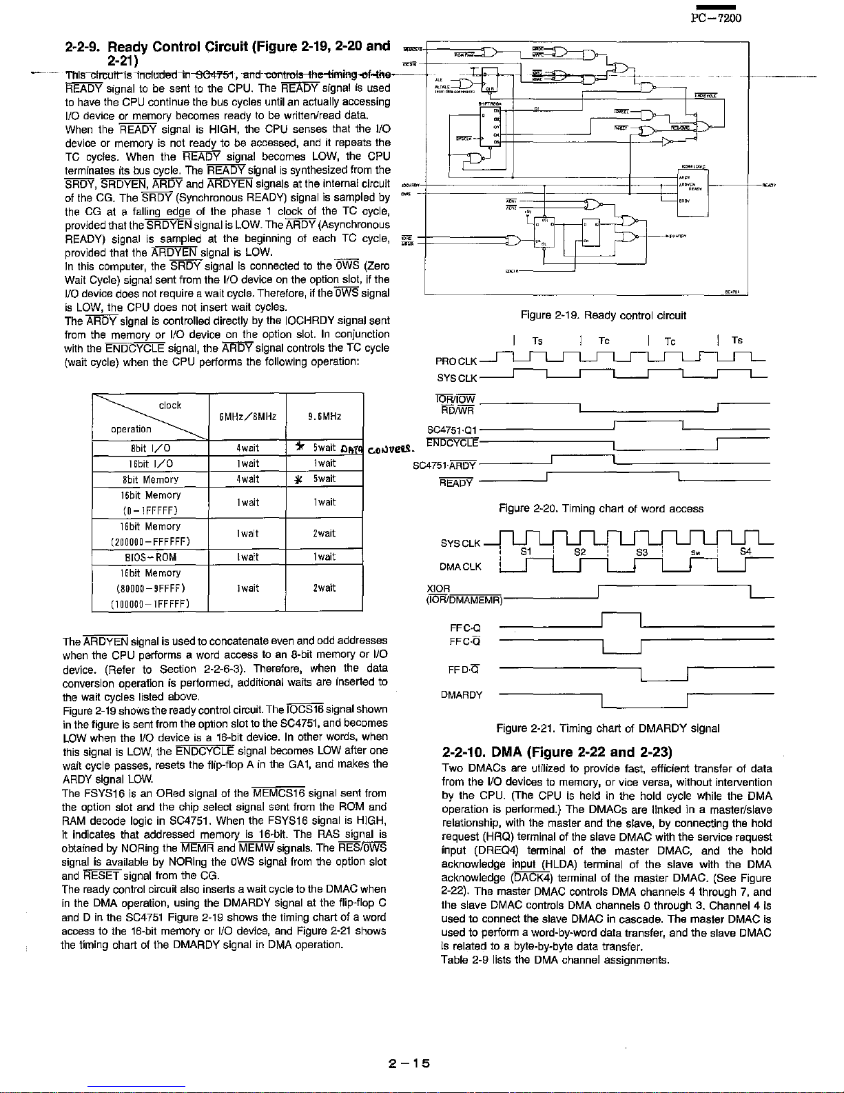
2-2-9. Ready Control Circuit (Figure
2-19,
2-20 and
2-21)
ThIs-clrcutHs irTcfuded-;n---se47''51 ,
-and-"'Controls-the-t1mif'lg~-tne
READY
signal
to
be
sent
to
the
CPU.
The
READY signal
is
used
to have the CPU continue the bus cycles until an actually accessing
lID
device
or
memory becomes ready to be written/read data.
When
the
READY
signal
is
HIGH, the
CPU
senses that the
110
device or memory is not ready
to
be accessed, and it repeats the
TC
cycles. When
the
READY signal becomes LOW, the CPU
terminates its bus cycle. The
'REAi5'Y
signal
is
synthesized from the
SRDY, SRDYEN, ARDY and ARDYEN signals at the internal circuit
of the CG. The
SRDY
(Synchronous READY) signal is sampled by
the
CG
at a falling edge of the phase 1 clock
of
the
TC
cycle,
provided
that
the
SRDYEN
signal
is
LOW.
The
ARDY
(Asynchronous
READY) signal is sampled at the beginning
of
each TC cycle,
provided that the ARDYEN signal is
LOW.
__
In this computer, the SRDY signal is connected to the
OWS
(Zero
Wait Cycle) signal sent from the
1/0 device on the option slot, if the
110
device does not require a wait cycle. Therefore, if the
OWS
signa I
is
LOW,
the
CPU does not insert wait cycles.
The
AROY signal is controlled directly by the lOCH ROY signal sent
from the memory
or
I/O device on the option slot.
In
conjunction
with the ENDCYCLE signal, the
AROY signal controls the TC cycle
(wait cycle) when the CPU performs the following operation:
~
6MHz/SMHz
9.6MHz
operation
8bit
I/O
4wait
if
5wait
OM"
16bi!
I/O
1wait lwait
Shit
Memory
4wait
~
5wait
16bit
Memory
(O-IFFFFF)
lwait
lwait
16bit
Memory
(200000-FFFFFF)
lwait 2wait
8105-
ROM
lwait
lwait
lSbit Memory
(80000 -9FFFF)
1wait 2wait
(IOOOOO-IFFFFF)
The ARDYEN signal is used
to
concatenate even and odd addresses
when the CPU performs a word access to an
8~bit
memory
or
I/O
device. (Refer
to
Section
2~2~6~3).
Therefore, when the data
conversion operation is performed, additional waits are inserted
to
the wait cycles listed above.
__
_
Figure
2~19
shows the ready control circuit. The IOCS16 signal shown
in the figure is sent from the option slot to the
SC4751, and becomes
LOW when the 1/0 device is a
16~bit
device. In other words, when
this signal is
LOW,
the ENDCYCLE signal becomes LOW after
one
wait cycle passes, resets the
flip~flop
A
in
the
GA
1,
and
makes the
ARDY
signal
LOW.
The FSYS16 is an ORed signal
of
the MEMCS16 signal sent from
the option slot and the chip select signal sent from the
ROM and
RAM decode
logic in SC4751. When the FSYS16 signal is HIGH,
it indicates that addressed memory is 16·bit. The RAS signal is
obtained
by
NORing the MEMR and MEMW signals. The RES/OWS
signal is available by NORing the
OWS
signal from the option slot
and
RESET signal from the CG.
The ready control circuit also inserts a wait cycle
to
the DMAC when
in
the
DMA
operation, using the DMAROY Signal at the flip·flop C
and D in the
SC4751 Figure 2·19 shows the timing chart
of
a word
access
to
the
16~bit
memory
or
I/O device, and Figure 2·21 shows
the timing chart of the DMARDY signal in DMA operation.
-
PC-7200
~
""",-=a.J-
:::::::~-
""""
-.
-
lOCH"'"
-
;o.c
-
~"'''~
,""1""0'
"
r-'
"
"'
,_o-
m
p--r"
PROCLK
SYSCLK
JOR/IOW
RDIWR
SC47s1·Q1
ENDCYCLE
-
-
l ,.,,",
"'
,
l;.
I
l!III;rr
I
-,::L>
~
-l-
~
,00,,"
'---
~
,""
""'n
>
t;n~~-"".~
""""
.""'"
Figure
2~19.
Ready control circuit
Ts
Tc
Tc
I
Ts
SC4751·ARDY
READY
Figure
2~20.
Timing chart
of
word access
SYSCLK
81
DMACLK
XIOR
(IOR/:"DM"'A"M"'E"'Mo'R)-----.....J
L
FFc·a
FFC·Q
________
~~L
__________
_
L-J
FFD·C[
DMARDY
Figure 2·21. Timing chart
of
DMARDY
signal
2·2-10. DMA (Figure 2-22 and 2-23)
Two
DMACs are utilized to provide fast, efficient transfer
of
data
from
the
I/O devices to memory,
or
vice versa, without intervention
by
the
CPU. (The CPU is held in the hold cycle while the
DMA
operation is performed.) The
DMACs
are linked in a master/slave
relationship, with the master
and
the
slave, by connecting the hold
request (HRQ) terminal
of
the slave
DMAC
with
the
service request
input
(DREQ4) terminal
of
the master DMAC, and the hold
acknowledge input (HLDA) terminal
of
the
slave with the
DMA
acknowledge (DACK4) terminal
of
the
master
DMAC.
(See Figure
2·22). The master DMAC controls
DMA
channels 4 through 7,
and
the slave DMAC controls OMA channels 0
through
3. Channel 4 is
used
to
connect the slave
DMAC
in cascade.
The
master
DMAC
is
used
to
perform a
word·by~word
data transfer,
and
the
slave
DMAC
is related
to
a byte·by-byte data transfer.
Table
2·9
lists the
DMA
channel assignments.
2
-'5
Page 22
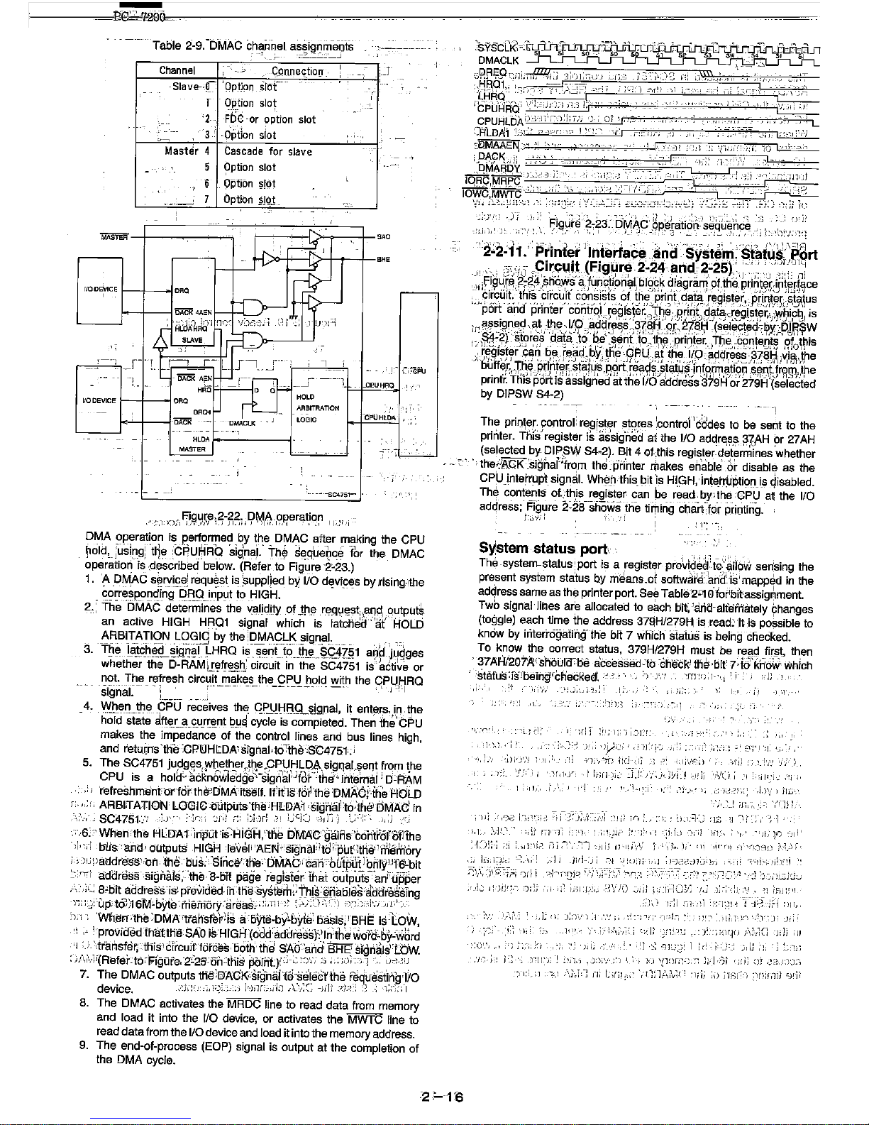
Table 2-9. -OMAC channel
as~iQI'),rn-eotS
l '-_ -:-.::...
____
'_.J
Channel
-
'--~
C,Qnneqtion
...
~.-
Master
r
qp_tion
slot
'2
FOe-or
option
slot
3
,opt
jon
siat
4
Cascade
for
slave
9ption slot
G 9ptjon
§i/ot
,>
:'-,-1,
n;',
F;i,~~,F?1~-~~;
19M~,
,0'p'er~t,i~_r
) i ,)1
'i
'"
..r;~UH~
~
i-'
DMA
operation is performed by the OMAG after making the CPU
~o'ld~j:lS~~_g;
't~e
:CPU,~R9
signa:I.'
th~
s~q:ue-~c~
for
the OMAC
operation is "described
b"elow.
(Refer
_to
Fig,ure '2'-23.)
1.
'A
DMAC
servicf3i request is
~upplied
by'I/O
d~vi~~s
by
Jising"the
corre,sponciing-ORO irlPut to
_HIGH.
2.
~
The
'[)MAC
d-etermines -the yalidity of
Jh!3:
r~q~~st,;al1d,
_output~
an active HIGH HR01 Signal which is latchett"
'at'
'HOLO
}\RBI-r:ATI()N
L()Glg
by
the'DJ'AACLKsignat..
'.
....
3.
T~e
La.tche'!.~ign~1
LHRQ
issenU,o.Jh_e.~g.4?§1
a~pjY<1ges
whether the
O-RAMU:!?f!~_~;
circuit in the 8C4751 is active
or
not. The refresh circuit makes the CPU hold with the CPUHRQ
-sfgnaC----
,"---
-,-
--.----
._..
,
j'-l".,
4.
WB~_IJ_~~e
__
¢-pjj
receives
th~
GP_l!tiB_Q..f?!g.nal,
it
ent~rs_,i,n,
the
hold state
aft~,r:..§L9..u!rt:!nt
g.!J~
cycle is completed. Then the'CPU
makes the impedance of the control lines and bus lines high,
and
retur:ns'the :CP.l!lHtOA1sfgnai,to:the
;S-C4751,;i
5.
The
SC4751
judgeswhether.the.CPUHLQ/!. signal.sent from
the
CPU is a hold'"
~cRn6Wi€dg,~-:msigrial:,.Jfb('thef"
il1'te'm~1
j
o'~R-AM
,,' 'refresnlfle'nto"f'for:ther:O'MAitsert If'it:i1n6hhe
:DMA'6hhs
f10l0
r:.
"; , ARBITATION: LOGIC:Qutputs'the
i
HLIDA1
,-sigil'al!'to-the) ElMA0 in
\\:,'
_ 8C4751./.'
:l.j':'
<I:" '.;i·! ,:, !:i-xl ,"!
lJ;;']~j
':-}Ii~)
!
..
;:-::'-~
j,;.l
<
.;',6:' When 'the HUlA
nnpUt
'is'HiGFi:l~~
bM~Cgains'i:oilWdr01I1he
)1'~,;
b-U's
:'and-!
dutputs
HIGH
'le'veP
'AEN~'si~inal;!td;'putqlie:~'ffie(n'6ry
I'"
)!'j~)addres'S1(bli,
:the,'bug,;'-,Sinci;Vthe:"CiMAC'-can""outptlt1biilyUf6':bit
':',:m) aCidress ;signals;-'the
-S-bff
page -register.
th~tt
outputs-ani;u~pper
r\
-"
':
,~;
_ S;bit
addres's,-iS'._
provided:
irfUie
~~ySierh;;
fhl~:~_Qa~Jes'
~ddYessTng
J~;
:,j!-Up)'ta,:16M~bYte
:mefiiory:areas';-'
';,nl-~:
; ,-').:_)'\' ']
',n-~,-,i';i
Ii
~",
-,'
'),1,
When-;lhe'DMA·tfah"sfeHis
ao\fte-by'byte'
oaSis/SHE
is'LOW,
'1
" i"proviCfed,th-aUtie·SAO
is-HIGH'(O'd~::~dCtressr)ln;'the'word~by';wbrd
'1'
'-tr'anSfer;:ttiis)6j'rcui(fdi"ces'-b~th'the
8'Ao'-:aii(j:
BH~
,slgnals'lb'w.
:
)f\('1]i(Refer-'to~F.igore'-2'':2S--6n--this
pointy
,j-,:
:7;,
:0,
,,:
;,),
-;,
i'
u,,)·
~:J
7.
The
DMAC
outputs
tlie'I}AC~sfghajt~seleiifihe
riic(lfiisiing'liO
device.
_"'j"1·>;;.i;~i_::--:;,,
I'·)jlr",i'lt) X',;(:
-)(Jj
,OJ_'-'::
:-;
_;
'1;;';,;,
8. The OMAC activates the MROC line to read data from memory
and load
it
into the
1/0
device, or activates the MWTC line to
read
data
from the
1/0
device and load it into the memory address.
9.
The end-of-process (EOP) Signal is output
at
the completion
of
the DMA cycle.
'2-2:11."
P~int~r
'In.te"ai:~
.aridSYst~ni;$t~iti,~;:~~rt
,]
],,'3)/']
,C:1r,Cl.ut
(FI!ill!r'i'2-24.and,~-25)."
',,"
,",:
"I
',)1
i~i,~~,~~.,~~:S~,s~~-~~
_~,
!~n,~io~c;tl)
bl~8~
9.iagr~f119qhe,
~~i~~~.~:~~rrt~ce
;;,;.9
i
!.?_ui!.,
"~i,~,
,?i_~cu}t
.~_C?~,s!~t~
,~f
,!~~
,pri~t_"
clCJt~,
re~is~er"
~PIt~trLS,~\'us
port and printer
cont~p:t,~e,~\~~er:_IT~~.;,p~ir:ltA:~t~(.~!:g!.~~~I\)Y'~~F~1
is
,,,~~si~n~~
,.~t)~~:
1'"11
.~?~rr~s,3,~~11
c%
2781;1(s~l~ct~<!'~Yo;pm~w
r;.,Yt?l_
,~t~r~~
_~a1a
;t~:,
~~
:~~n~;,!o_')t~'r
J)r~~t~r:.l~~~;~~~eu~
Rfo,~is
):,~~~I~!~r
'9~~"
q~"
r~-~~c
~Xi
~hr
_-9~U_;~~
t,h,~:
__
I.{p:
f1~q~e_~~
>~?a!:liJ~i1Jli\,the
biJffer_JhE!.p~inter;_stat.us
port reac!s.status-informatiorl
se~tfrom,
the
"(-"-)'-~-')
'lil.,,-
':),
'-"I)
""';,jo)
i'
'--;',)
,_'I.,
'.'OJ
:,-,
i--";'-'j.J
d.:u.',
printr. This port is assigned at the
flO
address 379H
or
279H (selected
by
DIPSW
S4-2)
I
• " I
'1',:')
,
The
pnQ~er.
~o.ntrol:
regIster stores ,control cbdes to be sent to the
printer.
Ttlis' register
i~dis'sig'ne'd
at the I/O
ad~r~~,~
~~,AH
~r
27 AH
(selected
by-
DlP~W
84-2). Bit 4 of-.this register-determines whether
'.
the~_ACK
.'siQIlaF'trom the',pri'nter
r-Oakes
enable
_dr
disable as the
CPU _ inte,rrupt
sign~1.
Whe,i"
this.
~it
IS
HI,GH,'
Iniefr.i.lpti9[1_
i_s
~isabled,
The contents
of.,.th,is
register can be read,by,the,CPU at the
1/0
ad!1ress; Figure
2~28-shows
the timing
chart~fo~r
pri(lting.
t-"VI i '
,-
,
System· status port
The-system-status'port is a register
provtde<:fto>',~llow
sedsing the
present system status by
means_of
sottws.r~;_lanct-is'mapped
in
the
adcjress same as
thE;!
printer port.
8e~
Tabltf2qO·'forlbit'assig~ment.
Two signal'Jitles are allocated to each
I::jjt~
'and-altefn'ately 9
hanges
(toggle) each time the address 379H/279HI-is
.read:,
'It is possible to
know by
intert6gatiii~"f
the bit 7 wfiich status is being cfiecked.
To know the correct status, 379H/279H must be read fir$t, then
, 37AHJ20-rA':shbulcrbe a'ccessed-lb -dfecl(! ttle-'bit' 7;id'kh6iN which
status
:rs!bein~ychecKed.
'-'
-,'
,-
;',"
'fTj
ii;;
i
"i
: j- •
:;!
,,, I,
-,
• .', ,_ i
-L ~ ,
,;
_1j.:.
I,'
'J!;i~"
,j-i!
" J,:;'
',;"
-ilL".'! 1 'I.:'
:li
n;",")f)
,':("]-,"
)iV~~)'
;,
~''-:
,,]i.
I'
:/,_
:_-'
;n,-;
,:
0
'(:-111
'
:-);)
',';'-:':;
L"I'-;;:'
;;j
':'~j:'T;;-';1
:'!,i
Jr-,),'
':,1,I.:r.;,
18
~I
I:
'-,.
--;
1
)'1.,
\1-',_"
i,jj
r-W'-l~
"j
';:',;1,"
:.":!
:ri::-j ,;i
:.>.1:)1,·0
,,)];-,',:)
'-'Ii_:
I;,g'-'/';
-,'
-I
-.,\,
.
')r)
j
.,h"21?
',:-)".;j":l'.'}
''-,r-;:-:
-
':'1'
--
---<'.
c·':2,-','.;l·;;1
:':)~:'j.:Jd:..;
',I.:; I ')/1';.-;
-"):~;
,I
J,'
;;-;r:j,.~,~
,'·;1,'/0
"::iiJ
;;,']H()~':
I,; ):'-;':;j.,'';,
~i
;!--;I1'"
,:.1;)
);,)
<J!'
:~i
'-;'1:_;1'
'Ti~
-jH
:
)1],
..
\;.
-'.'
..
':;
;,
:1'>1'
L;'
]"1]:);
I
:"1.~
.,):);'1
;:-)
\;
) ],.! \(l:)r;'1
;,:i
J"J,,::;,
'Jill
:.~i
,.~?,
:n:-;
~'1
'.:1
~
1
;".1' • .):]
(Ii
I;:rli!
..
",
l'):l'\;'v;!'
'1;jj
:i>
;'1;:;(---;
:,p;r,nj
':;Hi;
Page 23
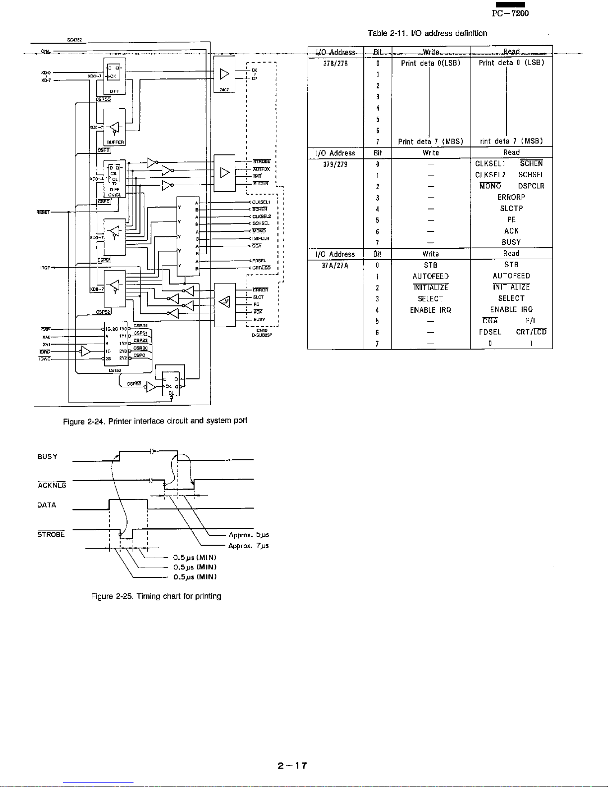
SC4752
r--
:~~
===~';;;'l';-~'
~
~-;:======:::t~~~
r--t~,~,,~",9··
:
'"
,
"
,
,
,
,
BUSY
DATA
,
t;~
,
BUFFER
"""'"
""""
mIT
"""'"
c_.
---_."
,
lKSEL1
;
,
,
,
""'~
,
,
SCHSEL
,
,
Sl'CLR
,
,
,
,
DSEL
:
,,"'"
,
- -
---
,
, '
,
,
ccr
,
,
"
""
,
BUSY
,
,
____
.J
Figure 2-24. Printer interface circuit and system port
I~
----+----i~------
r+--,~
---7--
-~
CN10
·SUB25P
Approx. 5)Js
Approx. 7)Js
O.5)Js
(MIN)
O.5jJs
(MIN)
O.5)Js
(MIN)
Figure 2-25. Timing chart for printing
2
-17
--II'O-Addr
......
378/278
liD
Address
379/279
liD
Address
37
A/27
A
-
PC-7200
Table 2-11.
110
address definition
-131
WI:
O_.n
0
Print deta O(LSB)
Print deta 0 (LSB)
1
2
3
4
5
6
7
Print deta 7 (MBS)
rint deta 7
(MSB)
Bit Write
Read
0
-
CLKSELI
SCHEN
I
-
CLKSEl2
SCHSEL
2
-
MONO
DSPCLR
3
-
ERRORP
4
-
SLCTP
5
-
PE
6
-
ACK
7
-
BUSY
Bit
Write
Read
0
STB
STB
I
AUTOFEED
AUTO
FEED
2
INITIALIZE
INITIALIZE
3
SELECT
SELECT
4
ENABLE
IRQ
ENABLE
IRQ
5
-
eGA
E/L
6
-
FDSEL
CRT/LCD
7
-
0 1
Page 24
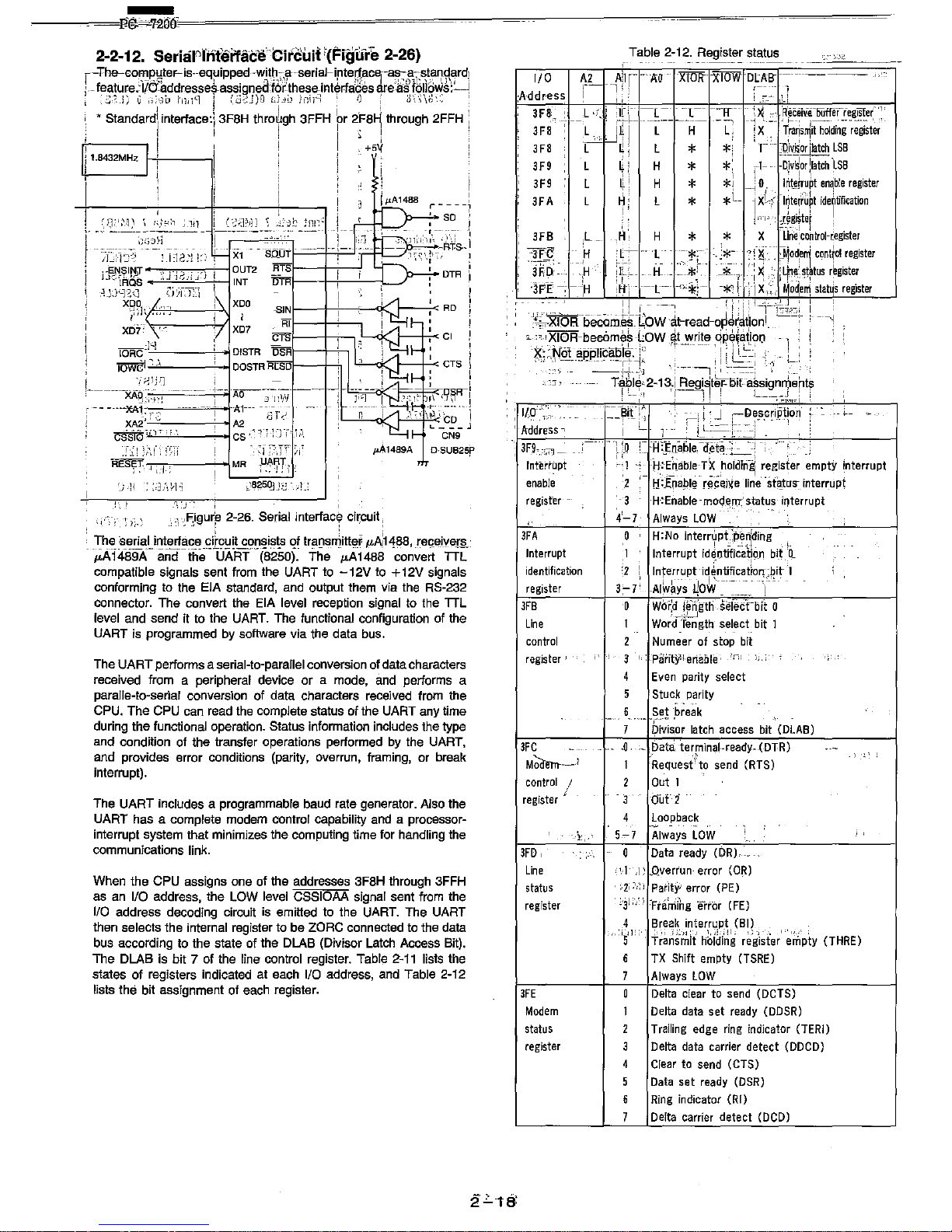
----~~B~------------------------------------------~------------------~
2-2-12.
Seriarfritei'faceCircuit'(Figure 2-26)
-The---cop~~~teF-
is.-eq~ipp~d
'.wl~~~:~f--seri~J-
i:"te~~c~--~;f;i~~!~~~\~rd!
_ feature.-I/naddressesassigned:forthese-interfaces are as
follows:---~
.:';,?,.1;
G
,;:-;;[1
flldl
:
(j·~1)O
Gf..:ll.!
)(;11':::;
i
i)
'
6\;',\1;"
,
I I
Ii!
i
; • Standard', interface:i 3F8H
thro~gh
3FFH or
2F8~
through
2FFH,
II
I I j i : '
I I
+5~
1.6432MHz i '
..
!=~N.SIW
::=ITITIT:r=j
L"-"lA:as
;lj"j'-E'J
X~?I
\F,R----p.,j
xDii'.-.~--M
IOR~
:~]~'-,
----+--1
lowc:I~',,"'----'-I
X1
fl_oD;--
OUT2
ATS
INT
ITm
XDO
-SIN
XD7
Rf
(;TIl
DISTR
DSA
DOSTRA[SD
-----XAB
-_~:-_1C".'!;--'==-+"i
'0---:)-:-1
;;;;'
-------XA1
...
" A1--
rJ1",J
XA2"
A2
e~rt"n':j'.
CS,'11<Ti'
1':'.
.~-;:
:r\(,
f;:;j
,I
;:--JT'
~,'
~,"'-;717.
-----'-->\MR
f~~T
~
__
,~8g50:l
H ',iL:
~',
I
r,.
--.J' I
DTR ,
RD
CI
CTS
pj.1489A
D·SUB25F
~
,".
~
-1-).F-;igU~!3
2-26. Serial interfact;'! circuit"
: The :serial interface
ci~cuit
con~i~ts
qf
trarasnjitte:r
1LA:1488,
reQeiyer§..:
·~1489A-
iiiiCf-the--UARf-(8250):
The
"A1488
convert
TIL
compatible signals sent from the UART to
-12V
to + 12V signals
conforming to the
EIA standard, and output them via the RS-232
connector. The convert the EIA level reception signal to the TTL
level and send it to the UART. The functional configuration of the
UART
is
programmed by software via the data bus.
The UART performs a serial-to-parallel conversion of data characters
received from a peripheral device or a mode,
and performs a
paralle-to-serial conversion
of
data characters received from the
CPU. The CPU can read the complete status of the UART any time
during the functional operation.
Status information includes the type
and condition of the transfer operations performed by the UART,
and provides error conditions (parity, overrun, framing, or break
interrupt),
The UART includes a programmable baud rate generator. Also the
UART has a complete modem control capability and a processorinterrupt system that minimizes the computing time for handling the
communications link.
When the CPU assigns one of the addresses 3F8H through 3FFH
as
an
1/0 address, the LOW level CSSIOAA signal sent from the
1/0 address decoding circuit
is
emitted to the UART. The UART
then selects the internal register to be
ZORC connected to the data
bus according to the state of the DLAB (Divisor Latch Access Bit).
The DLAB is bit 7 of the line control register. Table
2-11
lists the
states
of
registers indicated at each 1/0 address, and Table 2-12
lists
the bit assignment of each register.
Table 2-12. Register status
1 - - - - -
--
1/0
..
fil
r-
-AaXIORc
XIOW
DlAS-
;A-ddr-ess
" ,
I:
3 F
8',.,
__
'e
__
L
'I
~ i :ti~_
[ l -
---"11 ---
~
>i
R'~ceiie
Duffer
r'eglsfe{'l
3F8·:
~'.
i~
I
---i----H--
-L":
-lx
-
'frn~S~it
hading-r;gist~~'
3F8
: l
:....J
Ui
L *
*,
,--
~9~vioriJatc~LSB
3 F 9 . l
~
! H *
*:
1-
-
-D,)v~IOr
!,Iatch
LSB
3F9
L
~:
H *
*1
--:
0 _
1~t!!iruPt
en~ble
register
3FA
~:
L *
*L
IX~:~-I~t~~'ruftidettifiCation
! ''-1"' ,
:I~glster
:
3FB
L _
A~
H * * X
Line"corilrol-r:egister
,
:·JF~
_
JH
:L~
--
'l'
~
~L-
"
*-
:_j'~~.,-:-
~~odre~
control
register
3~~-
":H
iIf-;-""-H-------~:,
-~-?
:i~,-:
jL~~::~t~tusr~gister
'3"E
-;
-H
H'
---l-·
-"*'
_.
-*,.
hi
X,,:
..
"od'llI
slat"s
register
i
,L
, ' 1
,,'
_.,
"I , ,
'''l~
.. ' _"_
-,,,
i
_!
i.
-;
! i , ! i
Ll'---:I~~,~~:
i
~-~,
XIOR--6ecameslbw·at-read-oper~hionl.
~-.-:----~
>--
;,,'
XIOR-beeomes low at write
dJ?e~ation
-,
] !
*~;,:,,~OJ-~~_~!~C~~:[~j,;
.!~_=--~;)
L.~~:
.~:
"
L:~,
,':j
>
Ta6Ie"2~13.i
Regist~r-5irassignm~hts
ii.._'q
11'--~1!!
:
J:;
---'-:''''''',1
IICY·','
>
_~~!f:~
'. --i'
J
:-De.s.c~i_~t~on
..
>
'-
-l--
>
,
Address-:
' I
I -
1
..
: i
i_'-~:
t
--j
3F9~.':'rll_
.. : !o
,_
'fiJnable,
d,et','::"'::-',
'
"
Ii
Interrupt
1
..;
H-:EhabJe-TX
hOldin-~
register
emptY
interrupt
enable
2
,-
H:_fnaple
nicehce
line"st~ttrs-
interrupt
register
-
3
H-:-Enable-moQen:r'status
interrupt
,
4'-7
Always
lOW
3FA
,a
,
H:No
interryPt)e~;ding
,!
Interrupt
1 Interrupt identificati9n
bi_~
Q
identification
'2
,
Inrelrr~P\
i1~.~_~i~c~_t~0~.~~it
')
:
,
register
3:-7 '
-Always
~OW
_ " I
3FB
0
Wo-r,d
len'gtli
-ser~crbft
0
_,J.-J
Line
I
Word
length select bit
1
control
2
Numeer
of
stop
bit
register'
3
' '
parity.!'ertaflle'
:~,
:; :
4
Even
parity select
5
Stuck
parity
6
Set
-break
-".
,'.-
7
'~i~i~or
latch
access
bit
(DLAS)
3FC
-
-".
~.
>
Data
te~f1inal,.readY--(DTR)
M~·-'
,
1 Request'
to
send
(RTS)
control
/
2
Out
I
register
f
3
Ouf
t
4
loopback
~'"
.
5-7
Always
LOW
1 , ,
3FD
I 0
Data
ready
(DR)
line
'.1
,1
~
.overrun-
error
(OR)
status
' '2",:1
ParitYl error
(PEl
register
:'3
1
;
..
"
'Ftafrilhg
error
(FE)
4
Break
interrupt (BI)
'''5'''
:',,; ,:;-,1:' ',;:':11;
.;, . .-,
"',,-,' ,
Transmit
nolding
register empty
(THRE)
6
TX
Shift empty
(TSRE)
7
Always
lOW
3FE
0
Delta
clear
to
send
(DCTS)
Modem
1
Delta
data
set
ready
(DDSR)
status
2
Trailing
edge
ring
indicator (TERl)
register
3
Delta
data
carrier
detect
(DDCD)
4
Clear
to
send
(CTS)
5
Data
set
ready
(DSR)
6
Ring
indicator (Rll
7
Delta
carrier
detect
(DCD)
Page 25
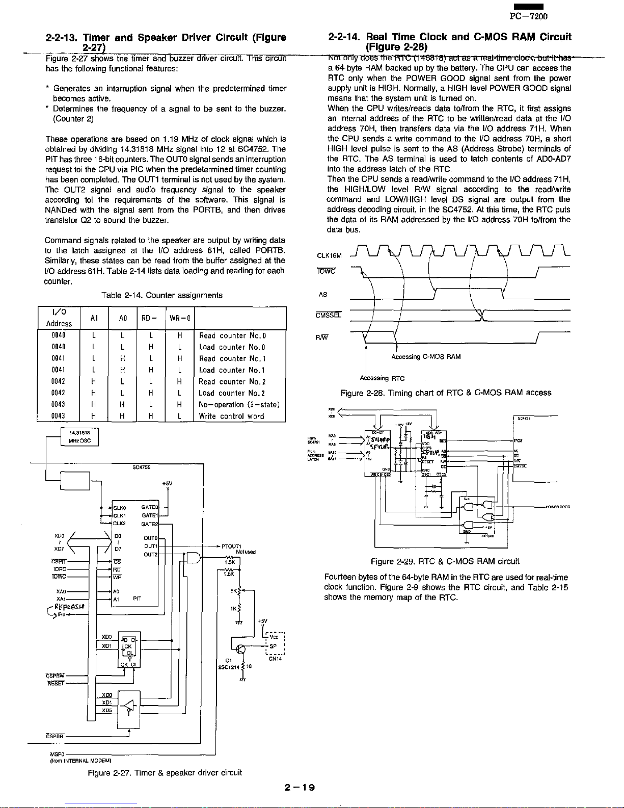
-
PC-7200
2-2-13. Timer and Speaker Driver Circuit (Figure 2-2-14.
Real
Time Clock and C-MOS RAM Circuit
___
2-27) (Figure 2-28)
Figure
2-2"7~sh~o~w;;;s"'th;;:e:-t;Cim=er;-;;an;;:d;n;b:;-;u"'zz;;;e'ro"nvcce'"rccc"I"rc"'u"II-,
"'1
h"l~s~c"',,"'c"'ulwl
------r:JrnLm'tVlloes U
Ie
F\Te"'(
1"4'581"8,
ael
as
a leal:ttime-clock;-truil"t
itit-ll
...
as.._---
has
the
following functional features: a 64-byte
RAM
backed
up
by the battery.
The
CPU
can
access the
* Generates
an
interruption signal when the
predetermin~
timer
becomes active.
Determines the frequency of a signal to be sent to the buzzer.
(Counter
2)
These operations are based on 1.19 MHz of clock signal which is
obtained by dividing 14.31818 MHz signal into 12 at
SC4752. The
PIT has three 16-bit counters. The QUTo signal sends an interruption
request toi the CPU via
PIC
when the predetermined timer counting
has been completed. The
QUT1
terminal is not used by the system.
The QUT2 signal and audio frequency signal to the speaker
according toi the requirements of the software. This signal is
NANDed with the signal sent from the
PORTS, and then drives
transistor
Q2
to sound the buzzer.
Command signals related to the speaker are output by writing data
to the latch assigned at the
lID address
61
H,
called PORTS.
Similarly, these states can be read from the buffer assigned at the
110
address
61
H.
Table 2-14 lists data loading and reading for each
counter.
Table 2-14. Counter assignments
I/O
A1
AO
RD-
WR-O
Address
0040
L
L
L
H
Read
counter
No.O
0040
L
L H L
Load
counter
No.O
0041
L
H
L H
Read
counter No.1
0041
L
H
H
L
LOad
counter No.1
0042
H L L H
Read
counter No.2
0042
H
L
H L
Load
counter No.2
0043
H
H
L
H
No-operation
(3-state)
0043
H H H L Write control word
---1
14.31818 I
MHzOSC
SC4752
---1
f--
.5V
-ClKO
GATEO_
__
ClK1
GATE1
c-
C,",
GATE2-
XDO
/ \
DO
OUTO
X~7\-
-j
,
Dun
PTOun
07
DU",
No!
used
""","-
~
""
-L/
1.5K
"""'-
-
""
--m-'
lOWC--
-
WR
XAO--
_AO
5K
.~
""-
-"
PI7
C;1:r'R.eS
u
"
IRO_
,j
.5V
-
~
4v;"--:
2QQ.-~
:
SP
:
~
CK
CL
~
--
-_.
0'
CN14
~
2SC1214
"
CSi'SW-
m;m"-
>00
-
~-1-
~
CSPBR
...J ----r-
MSPO
(from INTERNAL MODEM)
Figure 2-27. Timer & speaker driver circuit
-
51:475'
F.om
IIOOROSS
~,~
2-19
RTC
only when the POWER GOOD signal sent from the power
supply unit
is
HIGH, Normally, a HIGH level POWER GOOD signal
means that the system unit is turned on.
When the CPU writes/reads data to/from the ATC,
it first assigns
an
internal address of the
RTC
to
be written/read data
at
the
110
address 70H, then transfers data via the lID address
71
H. When
the
CPU
sends a write command to the liD address
70H,
a short
HIGH
Jevel
pulse
is
sent to the
AS
(Address Strobe) terminals of
the RTC. The AS terminal is used
to
latch contents of ADo-AD7
into the address latch of the RTC.
Then the CPU sends a read/write command to the
I/O address
71
H,
the HIGH/LOW level R/W signal according to the read/write
command and
LOW/HIGH level DS signal are output from the
address decoding circuit,
in
the SC4752. At this time, the RTC puts
the data of its RAM addressed by the
110
address 70H tolfrom the
data bus.
)
A~e";Og
C-MOS
RAM
Accessing RTe
Figure 2-28. Timing chart of ATC & C-MOS RAM access
"\"
m.
SC4'"
.:.
~
~" •
~,.
~
Figure 2·29, RTC & C-MOS
RAM
circuit
Fourteen bytes of the 64-byte RAM
in
the RTC are used for real-time
clock function. Figure 2-9 shows the RTC circuit, and Table 2-15
shows the memory map of the RTC.
Page 26
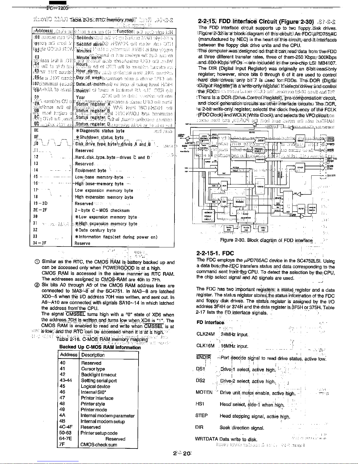
-
---=='I'€'"'1200;c=·
------~---------------------~---
t-:J\9,d.r,e;~,~J
,::.JJ')
',J;,'
~;--'-:J-:
.~
2.;
_
~
jJ
·'-Fuqctiqr:n
"l,:.'
~-,;,,_,~,
'r'IC:'j
;,~;.yl
~OO;
_'
;-::;~;;}S
i:":;')
',j-~:
)Seconds:;,:;~-.:J
.:;ri.'
-r:
:-,j;'
)k:
::J
;/i\n
)j'(!l--:-:', '-j
l[l!r·\).~j
~)f:J
;:",),1
'-Seccffii:falarm).:.)
,-j::";',}/,-;,-~
';);ii r:,):jI,'(
fi!:)
J;';:
i:Ol
e
.):'.:'!
c,':,';'.L)
~~-:'?'--'M-j~ufe~
i'~;,:
~;~
;i'~;---
)]::)i;-;
,:;j
Jinu" "'-;:'I!n
-,,-,
"--'1"',"
-"
1.
'" .
'.'
'-~"?
9,-1'
-,--,-"
,-
-J'"
03
Minute"ala-fr'n"'u,""
~.,-,
""")',1_
":_J_.,,,
,-,:,,-,_
..
~
t~,~-)i;:~7
1~;
;~')
J;i!)_
::2-'
:1.
H~Oy~~:~)
~,';)'n::J;.~~_;~~~;:::11\;~~)j,?:~_~'j;,;:.
:,:~~;)
."~~;:
__
)~;::J
-:':'~~
i,O",5
f
'I/\,'
ill''\:
22j";jJ'---;Hgyr~~IW~~b
,:,L;)
~·:i)c,.-
__
-"j
jj)li!'
;'jfr',
-:~o-:~!<-'
,;
RYr!d
.::;
,i '!il\'
;:.:;-,}"!i-:-
!.Oay,·;of,.
weJ~kb;
~:.;rr;rilO:i
<)j:T
..
'.'
;) ;:h:n:: ':Lj,
')
),!;
·1-1),7;;:'_"'.'-ri;;r;
z·:;
(~\:';-.)
];;
~
Datej~tif.;month
,:),;;
~:;
;;';:)~;
,)i
'),;l~_;q
I'"""
,,,--:,j;-]
09
Year
:
~~;ri'J~~
"
;'~:~h
':~'I'~'.~:;
)~~):~\~~~lf~j~~~~~:~';'I;~~~:~~~
1
~~J
~,~;
l8':i~~)-~;'
~~~:;;:
.],1'
);~ll;
,C)q~
fT:c,j)
j:-,,~jl:J
cH~St~;~~_:.:.-re~~:sJte'~)'~'jl
;
i.e::::
)"/jO,J
nr;,,; ·).T'H1f.;,Yl
}~:j
:::ri-i~
J,:i ,
..
Xi';'~
,_;~~,atll\s:r;~~I~!.7E~
C,IH
ili
,1JL;:"-'
j(jib_,:~:
,_,
:_>)li~b.;
.QQ
"'-";-',,);
,'J.-;-,
';.-0;'
~!a,~u~;:r~gi~tlilr.l~c)_o~'
::r),,,
,"I
'..-;
;~l'
"j
",,1.-,;';'
:11
DE
*Diagnostic status byte
_:;.:~j
."j;,,;)
OF
*Shutdown status byte
ji
O
'\_
. .J
.~_.
/DlsK);ri~~u~'~~
___
~yt~\:J!!i~~~
_r~hq
..
'8-
.11
_
Reserved
12
Hard_di,slc.ty-pe.._byte
,-drives C
and
D-
13
14
15
+6-
Reserved.
Equipment byte
Low-'.~base
memory-byte
-
-HigH-
base-me-mor}!--byte
11-
low
expansion
memory
byte'
1 a - - -
High
'expansion
memory byte
19
-20
2E-2F
30
31
32
33
34 -3F
Reserved'
2-byte
C-MOS
checksum
*low
expansion
memory byte
:':1.,
-:
.>?lTJ:U[h,~~x!?a~si9!l
;J;r:l,emo~y
b,vte
*
Date
century byte
*Information
flags-Cset
during
power on)
Reserve
],
G) Similar as the· RTC, the CMOS RAM ishattelY backed up and
can be a'ccessed only when' POWE;RGPQD is at a high.
CMOS RAM is accessed
in
the same manner- as RTC RAM.
The-addresses assigned to CMOS-RAM' are
40h
to 7Fh.
® Six bits
AO
through
AiY
01
the'CMOS
RAM
address lines are
connected to
MA3"'S-of the' SC4751.
In
MA3-8
are latched
XDO-5
when
the
1/0 address 70H
Was
written, and sent out. In
A6-A10
are C6nnecfed with sign'afs
SA10-14
in
which latched
the
addres~
frorri"'the
~PU.
The signal CMSSEL turns high with a
!'O"
'state of XD6 when
the
addr~~~-]9~l"j§
:Y':~l11f:,'i1.
sm.9
:t~rp~.
!~,!,
__
w~~,n,)~D6
is "1". The
CMOS RAM is enabled
to
read and write when CMSSEL is at
:
l:Hbw;':arid~:the-R1'(fban
Eie:
accessechvheii 'it'
is';'~f'
a:'higfl~
,
.~
':'
'Tablei'2~+6.
&~Mo'S:
A~M,:rh~~brYl~r'rt~~piri~;
),
-j
"
1-;
-,j _ •.
_
'i
•
!';
'.'
'1
'i
'",
,');
'il,'
Backed
Up C-MOS RAM information
Address
Description
40
Reserved
41
Cursor type
42
Backlight timeout
43-44
Setting serial port
45
Logical device
46
Internal
SIO'
47
Printer interface
48
Printer style
49
Printer mode
4A
Internal modem parameter
48
Internal modem setup
4C-4F
Reserved
50-63
Printer setup code
64-7E
Reserved
7F
CMOS check sum
2;2,.15; FOO.lnterface
Ciri:uit:(Figure~2'30J
,~J
1,,!>
The FDD interface circuit supports
up
to two
fIQPpy_.aisk
drives.
J
f;=igu
ref)
2~32Yis:~arblock,:diagramj
6t
this-:ciibuit!1
Arr,'
F-DC~;a.PD"l6qf.'iC
(manufactured by NEC) is the-_hea'rt:cifthis,circuit,:,'at1d;Jtinte'rfaces
between the floppy disk drive units and the CPU.
~rrh'ei
comj:mtei"~was~designed'"·sd~,thSltittc-an::re-adl-data
froin:thEnFDD
at three different transfer rates, three of them-250:Xbp-s;,,300Kbps
,'a:n-d::600rKbpslNFOs
:--_la.rel
ioi::luded
irp,thSl,lmeMcliip:t:.SI-:MB4rD7.
The
DIR
(Digital Input Register) was originally
an
BfbitJ:,ead,only
register; however, since bits 0 through 6 of it are used to control
;~ha'rcVdisk,rdrives;-~bnl~
bit:7 is
-used
'for::FDDS'..
Ttr~~DO.R
(Digital
<-:O"utput-
Regisfery:is
a'WrffEr-qnly:r.eg'isler"J
If
seleGtscdrive~··ar.rdl,control
,-th'e-:FD0c;~
.,
"
-~'::~.-:,~
L-,.1
,-W, ;-!
J,)
:~:'i
r .aJ',jJr:'y-x)
):::i-~j
1 a.'ll.-ij
<:;~rl
Tiel
::Thers:' is:
a:DCF.I:.(DrLve..Contro
I :
Regfste'f.,)',
'-pre.:compens-atibtr cirpoit,
an"d~'Glock!jgeh'eratioili.'circujts;as:}btf1Ehi;rnteriface:'t:itquits)
lihe:::DGR,
1
a:-2;.bi~w(ite-orily.,:register,;.sehi;mtS'
thEi~cIQck;
frequency btrttie
FGCK
(FDCClock) andcWCU«Write <!:locl<},andSelects the
V"O~ifc"it)oB
:]'i:jL)
.:-;:);!l
~:;:.'3
,~{:-;::(r:-i
:j;-!j .-,;'):1
j!j-j,,~
:~;;;D!:;
If;)
JdNJ
~)~-)C1:ilA[;1
"
.,,'
,---,
:-;:;~:::'r,-i~
;_:;J:;1i;:,~
::~,~,!;:,,!"~~
.1';":'==:J~==E:3f:;=~:;=;==~~';===:::;T,uJ_i.l:'"-
I'
"~"'"
~==;~"j'rg;
F:igure
2~30.
Block
d[~g!~m
6f_F5o.il]terfac~
_
2-2-15-1. FOe
,
,~
c_
••
'--
The FDC employs the "PD765AC device
in
the SC4752LSI. Using
a data
bus,,\the-E.QC
~ansfers
status
a~d
data corresponding to
t~e
command sent
frorn--.t~CPU.
To
detect the selection by-the-;CPU,
the chip select signali ajld
AO
signals are used.
The FDC has two important
regiS.f~~s:,a
stafu~,r~gister
and a data
register. The status register
stor.e~lt!1t3_:status
information of the FDC
and floppy disk drives. The
E\tatu1s_,
register is ,assigned
by
the
VO
address 3F4H or
37414
and the data rt3gister !s)3F5H or 375H, Table
2-17 lists
th~
fP
__
ioterfac,e Signals. ' -..
FO
Interface
CLK24M .
24MHz input.
CLK16M . 16MHz input.
ENI:lIR
DS1
,
,
;;'Port
~ec~de
~ig:n~1
to read drive
statu~,
?ctive low:
drjv~
1
s~le~,
~ciive
high.:
;,
,:
I
prf~e:2
selec~,
active high.,
DS2
I
_,I
MOTEN ,1 Drive unit;
mo~o~
ehab/e, active-high; . )
...
",
- """, 'ii
HS1
, '
):
'--
-
..
'
Head I select. $ide-1 when
high_.
STEP
Head ,stepping signal, active
hig~.
DIR
Seek -direction signaL
WRTDATA Data write to disk.
'--',i,
l):)l.Oi
-J
Page 27
WRTEN Write enable, active high.
--
~~-
maexpU1se Input from drlve;-actlve1ow:---
WRTPROT Write protect indication, active
low.
Head
track 0 signal, active low.
RDDATA
Read
signal from
VFO.
WINDOW
Read
data window signal from
VFO.
MFM
MFM/FM discriminating signal (MFM: low).
MINID/STD
Mini floppy disk/standard floppy disk select output
(standard
floppy disk:
lOw).
DA
Output
to
indicate the
MB41
07 external VFO data field.
VFOCLK Clock output
to
external VFO
MB41
07.
FDSEL Internal
FDC
address select input.
03F2H-03F7H: low
0372H-0377H:
high
CLK19M 19MHz input.
CHGFLT
VFO external resistor select signal. Low
in
the 2DD/2HO
mode.
TABLE 2-17.
FD
INTERFACE SIGNALS
2-2-15-2.
DOR
This register selects drive A or
B,
controls the drive motors, reset
FOC
and defines whether
to
permit
an
interruption
of
the
FOC
or
OMA
request or
not.
The
OOR
consists of
16~bit
flip-flop circuits. Description for each bit
are listed in Table
2~18.
Table
2~
1
B.
DOR
bit descriptions
I/O
Bit
Description
Address
3F1
0
This
bit selects
the
disk drive.
LOW:
drive A
(drivel)
HIGH:
drive B (drive2)
I
Low
level
of
this
bit
enables
the
drive select
signal.
1
FDC
is
reset
when
this bit
is
LOW.
3
HIGH
level of this bit allows
FDC
interrupt
and
DMA
request.
4
HIGH
level
of
this
bit
enables
the
drive motor
and
the
drive A
can
be
selected.
5
HIGH
level of
this
bit
enables
the
drive motor
and
the
drive B
can
be
selected.
Data transfer between
FOO
and
memory
is
executed by the OMAC
and
FOC.
The
FOG
sends the
OREO
signal to OMAC when data
transfer to/from the
FOO
becomes enable. This signal delays four
2MHz clocks
(2
ms)
for adjustment of
OREO
timing. After the delay
the signal is sent
to
the
OMAC
ORE02
line.
After passing through the tristate gate, control
is
done by the bit 3
of the
FOO
control register.
When the
OMAG
receives a
OMA
request from the
FOC,
it places
the
CPU
in
hold state,
and
then sends the OACK2 signal to the
FOC
after it
is
ANDed with bit 3 of the
FDO
control register to begin
data transfers.
When the
byteMby~byte
base data transfer
is
completed, the
FOC
sends
an
interruption signal via the IR06 terminal of the
PIC.
In
this
case, if bit 3 of this register
is
LOW,
the
OMA
request and interruption
are disabled.
2-21
-
PC-7200
2-2-15-3.
DIR
The
OIR
was used
as
an
B~bit
read-only register assigned at the
170
address
3f/H
or
377H; however, 7 of 8 bits are reseNea
fbt
hard disk drives
in
actual use. The CHANGE signal selects this
CNG
signal. This bit
is
active unless a disk
is
present and a step
pulse
is
received
when
the drive is selected.
2-2-15-4. DCR
This write-only register
is
assigned at the I/O address 3F7H, and it
selects the
VFO,
and
sets the condition of the FCLK and WCLK
signals. Table 2-19
lists the bit assignment
of
this register.
Table 2-19.
OCR
bit assignment
Transfer
FDC
Write
Applicable Applicable
Bill
BilO
Rate
Clock
Glock
Drive
Medium
l l
500
Kbps
8MHz
lMHz
1HD
1HD
l
H
300
Kbps
4.8MHz
0.6MHz
2HD
10
H l
150
Kbps
4MHz
n.5MHz
10
10
H
H
250
Kbps
4MHz
0.5MHz
10
10
Because the data concerning the disk drive type
is
stored in the
RAM
of the
RTC,
the
CPU
read~
the data before it accesses
FOOs.
Then the
CPU
writes the data to the
OCR
to select the VFO and
to set the LOWDEN. WCLK.
VFOCLK and FCLK signals. A 2HD
FDO
can
also read a
20
medium.
2-2-15-5. Clock Generator Circuit
This circuit
is
included
in
the SC4752, and generates the signals
listed below.
FCLK
A clock signal for the
FOG.
It
is
switched to one of B MHz, 4.8 MHz
and 4 MHz
by
the
DCR.
WCLK
The
FOC
synchronizes write data with clock signal WCLK. The
frequency of the WCLK signal can also be switched to one of 1
MHz.
0.6 MHz and 0.5 MHz by the
DCR.
2-2-15-6. Data Separation Circuit
Using the VFO, this circuit generates the window signal to separate
data bits
and
clock bits from the raw data read from the
FOO.
VFO
used
in
500Kbps, 300bps
and
250Kbps transfer rates are included
in
the one-chip
LSI
(MB4107) respectively. Table 2-20 listes the
assignment of the
VFO.
Table 2-20. VFO assignment
FDD
Medium
Transfer
Rate
ClK
Bill
of
SitO
of
WClK
DCR
OCR
2HD
1HO
5nn
Kbps
8MHz
IMHz
l l
2HO
10
300
Kbps
4.8MHz
O.6MHz
l H
1D
10
250
Kbps
4MHz
0.5MHz
H
x
2-2-15-7. Pre-compensation Circuit
This circuit
is
included
in
the SC4752,
and
advances or delays write
data sent from the
FOC
to the
FOO
according
to
the write data
pattern. The
FOC
changes the -status of the
PSO
and
PS1
signals
in
response to the pattern
of
the write data sent from the CPU.
Figure
2M31
shows the timing chart of this circuit.
Table 2-21. Write data pattern
PSI
PSO
Write Pattern
l
l
Normal
l H
Late
ODD
I
or
110
H L
Early
10000rOli
Page 28
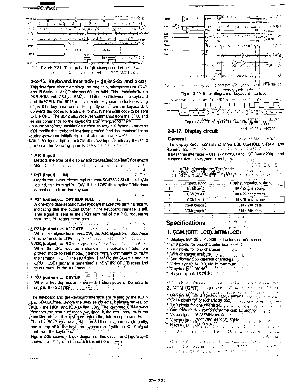
-,
~------------------------~-~===---=~-~~-
----="R€L';'1-200T'"
PSO
PS1
-",'
I
I
Shift \
"
'"
,-+7''''''---C~..=;~...",.rc.J~n.C·
: n ;'i
~Figure;·2~31lrrriiTling)'chart~of;pre~b0m'pensatfO'ri
cirCui~-;.-;:
'
2-2-16. Keyboardlnterfac&{Figure:!-32 and 2-33)
This_,-.-i~terf~ce-.
circl:dt-:emp1o.Ys--
,tlTe
.
p~e~Ghi~-i~rnJ9r~p-rocEf~"s"Or
8742,
and "is' assigned 'at
1/0
addresS
60H,or 64H. This:processbr.:has a
"
"t
.-
_
'C,
__
;
",;
I
,I;:.,
. I
2KB-
ROM-
ahd
-128-byte
RAM,
and,
[nterfaces,-,between.
the-keyb0ard
an~
tHe,CPU.
The 8042
redeives
serial
key'-scan
:codesico~si&ting
of
~an
8~bit
key code
'arid
-~
1-Qit
paritY
senf:from;thEt
k~yboard.
It
copverts
th~
codes to
la
parallel:
fanTrat
sy,stem
sca~
cdde:to
:be
~ent
to
.the
C:PU.
:The-:80~~
aJsp:receiv~S_',Gom,m_~nds;frqm
,the~CI?:U,
land
se~crs
commanas
To
-tfifi'keyboarCfafter
inte-rpretinglfleri\:-'~---'
"[In
:additiori·~to~
'the:'n:'mctions'
'describe:~I"."
abovepthe ·keyboard-.interface
~
caifmodifyjhe
keybb'ard,
interfaceeprotoC6r'andi
tne
keyrs'Can'cocfes
;
);durfrig·,.power",on-:!
initfaliiing.,·l[jj c;l ;,j','-;')
}ji1
;.;
:);:".'N,
.U:·j;") 'j:':' [
-,
'!;
.
J.Witt:1\
th'e:;
fQ.rrr
outplltderniinars;ah'd"tWQl~iripuet~Hiiji1alsi;
ttie'.'8042
performs the following operations,i;')c,n:1: '1.->1';
,'1
,!_.
'y
• P16 (input)
Detects the type ofaJ!!lisplay-adapter!ce:aaing;Jhe"Stafusof·switch
";-:S:-2.')i:~'
,nw'
i',',
,r)
,'j
I;, !-,,)').I:
• P17 (input)
...
INH '',I:',;
::Read~:the
:sfatus:ofcthalkeylock'.f,on:vSC4752·LSI",'I.fthe keylis
locked, this terminal is
LOW,
If it is LOW.)tlll8!,k'eyboar'crinterface
cancels data from the keyboard,
" P24:(outputl, ,
.•
,;QPT .aUF
~ULL
;
A,
one~byte
data-,senUrom
,the;
kyboard
makes'
this
termil'1al.
a,ctive,
indicating that the output
buffer,
in
the!'i
Keyboa~d;
ineJrfaGe
is
fLi11.
This signal is sent to the
IRQ1
terminal of the
PIC,
requesting
that the
CPU
reads these data.
~
-,
.-',.'
"j
<~,
P2l,{outpu!)· ,,,,A20GATE,,, .
I,
'"
i.""
.),
: 'Whetfthis)
signa.i-:becomes',
LOW,,:the~
A2Q:'signab
cm;.theiaddrsss
:.u:,bus!:iSlforce,d;to--LOW,; dl_:.:;:i-'
;,,1.>
-.;
:i.!'),,:
';;'j~j)n;;:·
:'11;
:,.-~~
p2p),,(o~tPlJt».!.,,~R_C,"\"-.'iJ~-n2.''''
(\~'. '-~\,r
~e~'
.~,
',.-:-,---,
-:\~\i
When the
CPU
requires a change
in
its';'operation.
,mode;
from
protect
mode
to real
mol;!.e,
it
sends certain commands to make
the terminal
HIGk
tke'Rt'~igrla:hs'se;;t'jto
the
SC4751
and
the
- • 1
~RP
~E~~:~~ighar'is
,gener~tecf.
"Ff~~lIy'-:
the'
CPU
Isireset and
thus
return~
to the
real-'
mode:
1
,)
, -
.'
,
""',
'.'
I
•
P23
(output)
..
i.
KEYINt>
si-:'
-r ' i
":
When;
a key depressibri'
Is
s~:n:~edj
a
s'hO'rt
pulse of
IQw
5t~te
is
~enttbtl1e
Sc4?~~,
'.,
i,
..
_._,
<~'.
L.
_ '
'.
The keyboard and
the:_keyboard-i~terface,
are,
relatetl
by
the
KCI:!K
",,~~9
_-'~DA
~A-!ine~_
Before~th'e
"8042
--seri~~-cja!~;~k~l~ay~,
nl~·~e$~i~e
,,~qLI5
!i,~e
HIGH
andKDATA
line~9"V;,
T;h~.key~qeri!;C;HIJ,a[",~ys
',,~?".i~o~;J;h~
..
sJa~lI,S:
9!
,th'~~~:J~~
UP,'1s:-:,If),!h~,)~q;
Ijne:!?ra~e:l
!~':me
\ 9
qn
p
i
t':9,n
;8:~9:v~,.
!~~-;~~ybSl~~,9
~me!1:i
!~je;j~~~aJ~c~ptiQrH')1~d.~.
,:
Them
the 8042
~!9rJg!;La,~"~t,'llr;tb,ik~n
~:,~i,tL~a~~;
<?;'p[l~bit:09q"P'q~iW,
and
a stop bit to the keyboard synchronized with the KCLK signal
sent from the keytioa'r&',i
',i.i0
');::'jj
j
~.,,;
i;·
];'11
Rgure'-2-39"shows, a
-bJoc~di,agram
of this circuit,-
aml,
rigu.re·,.s~10'
shows·the timing cnaitJj'n
data'transmjSSion,;-.~-:-~~
,-
'.'
'
~ESIIT
'""
,
,",
-:--i~~Lg]~
;"
';'1;)11>:i",\:
;!.:
Jj!
I)
2-2-17. Display circuit
General
The display circuit consists of three LSI, CG-ROM,
V--'l~Mdl,nd
]SbinE{~lS:.
'I'
','},
'_,
,.,",
t;·.'
!.l-)j",
';;~i,:J!
!;~'iBl.'8
r)7/
TJ":,:,,;-
It
has three interiaces - CRT (720x350) and LCD'(640x200) -
and
supports five
dlspl?lY1iFT;l~pr;$1~S'I~~lo~.
MTM(text)
CGM(tex.t},
.,,"
,
CGM(text)
4
CGM(grapbic)
,
640
x
2~0
dets
CGM(graphic)
350)(
2QO
dets
,
j'
. Specifications
.;;
"J:,
':
)
1.,C;GMCCaT,
J
..
CQ)'JIVITIIIII
(L.CO)
....
, * Displays
80'><25
or;4b~'2'5~ha:tacters
on
bri'e'screen
* '8x8'-pixel's::f6(cine':ch'aracter, bdx -
: *
7x7
pixels for
one
character
\Wi~.~;
9.~af;"m~~!,~tt!i!?l!l~,!
,'-::
:in,
';j
>.i",
J:
~~)!.
*
Can
display 256
,~i.~,~r!1m
~h,ar;~qt~rs;:l
/,"
~
Video
signa!:
14,31~18MHz
maximum
*AV-syh~dSJgW~I:';'6i:lt~{i':!
!I>
:1',; .',
-';..-h,
'.
":,
• H-sync...signal,-15J5kHz'.
'.,',.
'"
2.;"M1M
,(CRT),' i
!'l
>Jr'"
',.",
!"
:,:.)
:6,s~(~y~
80'j(.~5.~&hkr~bt~'r~'
;irr~nl~':
~6~~~~,~
,'::,:::'
j:
i,
<,
,;
'J)
-,,'J , ',,, \ ,'"
n'
",J
'~-'
."
"-'
."
",,'
..
1;
",-,. " '.' , ..
/ .
,'-""
.,'
,',
J;:) -'.,'."
.
."
9x14
pIxels
fo(one_~h~rl3<?t~~.,~o~):,,;.)
",-1;
~~
·t':~-j
~i'
."
,7)'$91p'?,els.forq!1etcl1~racte.r
,,,,'
,:',
.'
'\
.'."
,,1'
,;1,,:-
*
'bah
drive
'an
18kHz~ni·onbch'rtllneJdisplay
~bhit6;.,
,
,'}'
.
*
Video
signal: 16.257MHz maximum ,),
",j"
i""",
y-sYnc.sig~a!;,72Q:,35Q,(H.XY),
5QH~".
' ,
.,i,
, '.
,','.
'*
H~s'y~c-'~)g~ai:~,1~;4~2ki{t'
",',<
.. ; -',
,'"
-;"H1
!
..
, "
."
"'''','
---',',
...
J
·,11..
.'
".n'"
'-'
'-,
.J!
. < )
,)(!
:
ii.:"
,.
L'
",'
.'
.),;
..
;";
;.),.
"I
',i"1
Page 29
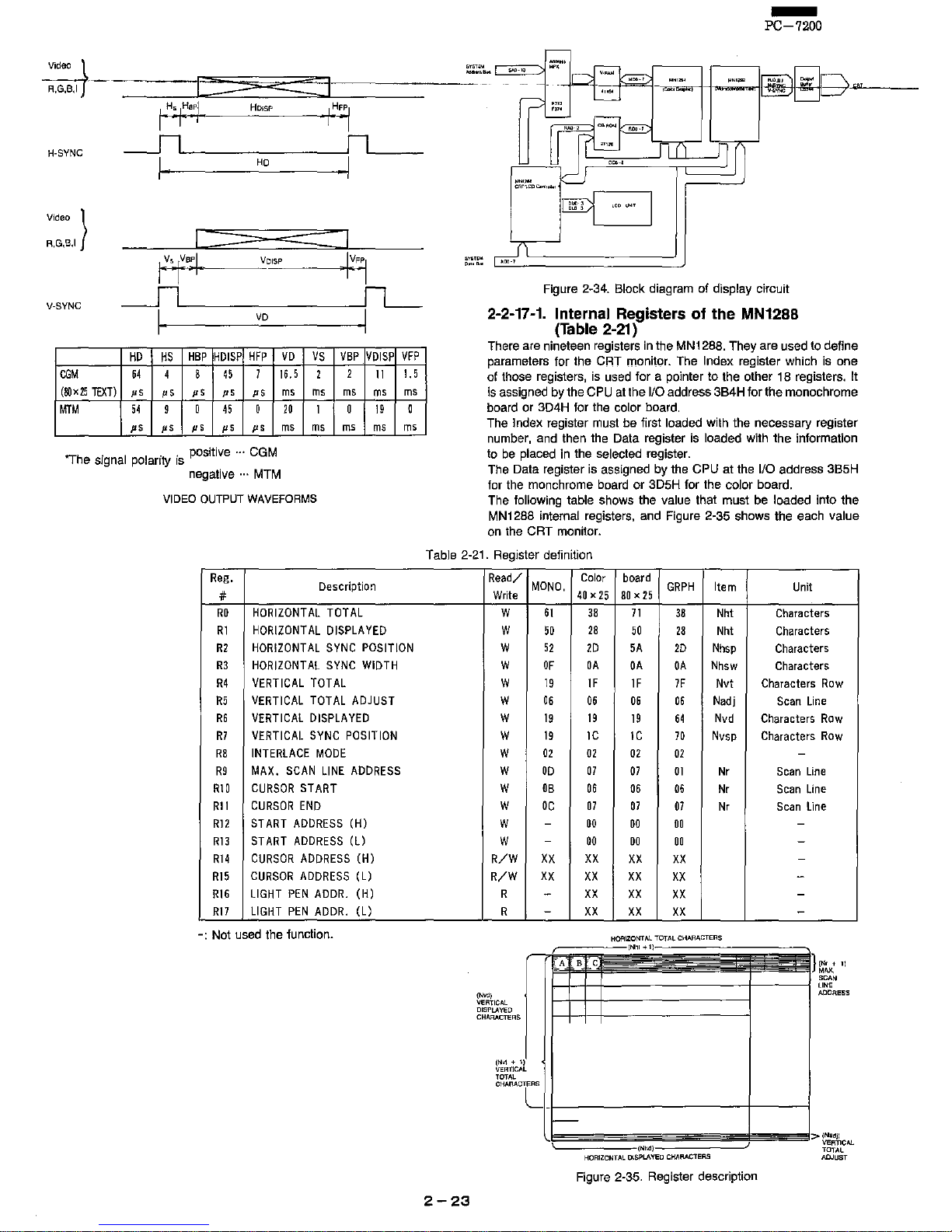
Vidoo
t
R:G."0
-
I
Hs
IHapi
HOlsP
I
HFP
1
1 I ' I 'I
H-SYNC
----Il
_____
--'nk-..._
I
HO
.,
Video
}
R,G,B,I
VOISP
V-SYNC
VO
HP
HS
HBP
HPISP
HFP
VD
VS
VBP
VPISP
VFP
CGM
64
4 8
45
7
16.5
1
2
II
1.5
loox25
TEXT)
"
"
" "
"'
m'
ms
m'
ms
ms
MTM
54
9
0
45
0
20
I
0
19
0
,s ,s
" "
"
m'
m,
ms
ms
ms
_ . . positive ... CGM
*The
signal polanty IS
negative ... MTM
VIDEO
OUTPUT
WAVEFORMS
Reg.
Description
#
RO
HORIZONTAL
TOTAL
RI
HORIZONTAL
DISPLAYED
R2
HORIZONTAL
SYNC
POSITION
R3
HORIZONTAL
SYNC
WIDTH
R4
VERTICAL
TOTAL
R5
VERTICAL
TOTAL
ADJUST
R6
VERTICAL
PISPLAYED
R7
VERTICAL
SYNC
POSITION
R8
INTERLACE
MODE
R9
MAX.
SCAN
LINE
ADDRESS
RIO
CURSOR
START
RII
CURSOR
END
RI2
START
ADDRESS
IH)
RI3
START
ADDRESS
III
RI4
CURSOR
ADDRESS
IH)
RI5
CURSOR
ADDRESS I L)
RI6
LIGHT
PEN
ADDR.
IH)
RI7
LIGHT
PEN
ADDR.
IL)
-:
Not used the function.
"',""
""
....
c9
'-----'
-
PC-720D
Figure
2~34.
Block diagram of display circuit
2-2-17-1.
Internal Registers
of
the
MN12BB
(Table 2-21)
There are nineteen registers in the MN1288. They are used to define
parameters for the CRT monitor. The Index register which is one
of those registers,
is
used for a pointer to the other 18 registers.
It
is
assigned by the
CPU
at the
110
address 3B4H for the monochrome
board or 3D4H for the color board.
The
Index register must be first loaded with the necessary register
number, and then the Data register
is
loaded with the information
to
be
placed in the selected register.
The Data register
is
assigned by the CPU at the
110
address 3B5H
for the monchrome board or 3D5H for the color board.
The following table shows the value that must be loaded into the
MN1288 internal registers, and Figure
2~35
shows the each value
on
the CRT monitor.
Table
2~21.
Register definition
2-23
Read/
Write
W
W
W
W
W
W
W
W
W
W
W
W
W
W
R/W
R/W
R
R
(NV01
VERTICAL
DISPLAYED
CHARl\CTERS
MONO.
Color
board
40 x 25
80 x 25
GRPH
Item
Unit
61
38
71
38
Nht
Characters
50
28
50
28
Nht
Characters
52
20
5A
20
Nhsp
Characters
OF
OA
OA
OA
Nhsw
Characters
19
IF
IF
7F
Nvt
Characters
Row
06 06 06 06
Nadj
Scan
Line
19 19
19
64
Nvd
Characters
Row
19
IC
IC
70
NV5P
Characters Row
02 02
02
02
-
00
07
07
01
Nr
Scan
Line
DB
06
06
06
Nr
Scan
Line
DC
07 07
07
Nr
Scan Line
-
00
00 00
-
-
00 00
00
-
XX
xx
XX
XX
-
XX
XX XX
XX
-
-
XX
XX XX
-
-
XX
XX XX
-
HORIZONTAL
TOTAL
CHARACTERS
~~~~'
..
,~------~
(1'1,
+
11
.""
,~,
I-+--+--+-----------f----j
~~RESS
HORIZONTAL
OISPLAYED
CKI\RIICTERS
Figure
2~35.
Register description
Page 30
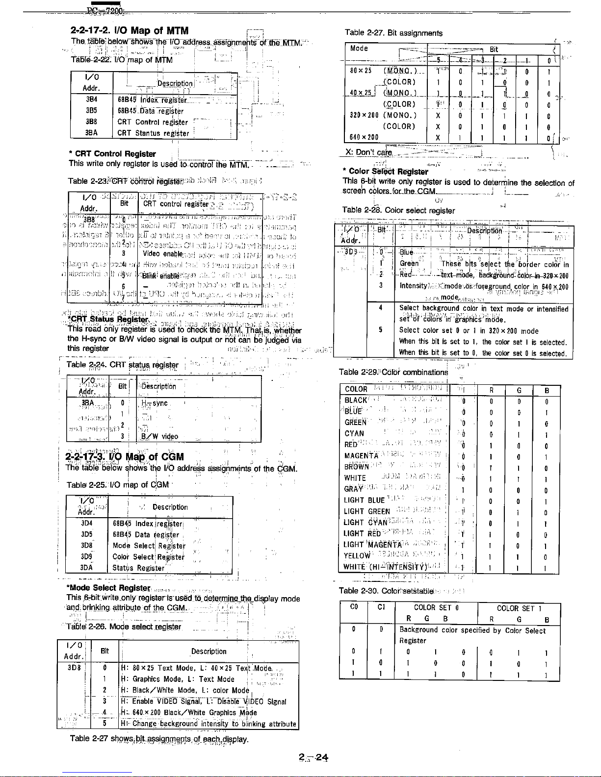
-
--
____
~_~n~~~~-------------------------------------------------------------
2.2-17-2. I/O Map
of
MTM
"
!he
t:a~Iej,b~I?YfSfl~~s-t:h~-T/2~if~r-e~~~,~SSighm~rt§:'~nlJe]lj1TM;·
c,
i
",:
:',"',.':
,:
',,',-
__
,-
! i
_'';
1-
,.'
I '
Ta51e'-2-22'
1/0
'map of
MT.
M '
>. -..
: ,
" ,
I '
,
I/O
I
' I
",1'
I
D~_!;.!;ri~t~o.~j'--
'C, , _,
..
Addr.
,;=eo--
3B4
68B45
in~ex,
re:grste'L~~
-
3B5
68845
jrata
Jeglst~r
3B8
CRT
Control
regi~ter
c·
.
!
3BA
CRT
Stantus
regi$ter
'*
CRT Control Register i
I
,------------.
__
••
_______
_
This write only register is used -to--control the MTM. _
Table 2-23jrG"Rli control'
regTstEifJ-';ib
~b-\in
i','
li:-;I
'-;-I/7,;O:-:-:)C",r:"~lC~~.
,"';."T~".-j"J"'.7';,':')
-c
__
":-_-:
~-~..,,~.;-,
"'''~;-.'';
,""
-."ee,
n-,",:";
s-·,.....,
-
'~·t
<>~~
Bit
CRT
control
registe~'
2
'--'
Add
...
.
.;"'"-'\
____
.J"
/
"'3-S8
r,,";
--.1":0
T_,i
I
..
0-->'
,'j;"
';)'"
'I,
.,"
,-;;
"'-17!: I
'~'-_;J
J
,;"
_11,;
')
;'l,.-j r
'~n
;;1
T,;~:j;';'/
,::J3j'='3~
;,8;:;'i]
!-i,iT
nl.,u'il
r;'~:'!
.-,;'; :
I,
A;
~,-ji;):;'!:,q
j; . ;';,t;.w;::n
31
,''ll-iiG
i:
iT
,)J
n1;
i:
_,
i
:,'
iy)'!
:_:1
,
''1
:0,
te)
0\:10,fi:J'~:-:~;i,'
;,-ilbi;
,>S>;2'.;3:i.;:-_~;;';'i-.1,~:Ji.,:.!
j:)'-,,:J--'-ji
0-:""',,'::
3
Video
enal;l!e;-;
;'1
;;)1.'," 'i'l1
:.:'.[
f ;':
'-!-
10
':
:
3c!:~y-Jl
(:.
n.~41
';1)
Fkl'll ;)',0.0')1
~--!;,
j'!;
'::I~i
:';{~rJ_
,li
-,
,I
,1
;l;;i:l:y-,li-;i
,-)
]j
I
i~';j
:
'-'SlrriR:
enabT~k:H'11
. ;
iJi
i.,
, ,
~:
! ,j -
'l
i; , ;',
,r:'i
'J',',::
.-
_,:~;)
___
;
!''-;~:,I
1.
'-' _II;;
,,'
-l,"
",'/'1,1_,
J:.,_.,
I.ill
..
,)""
.lrl:
'4~':~~~~~~y~~~~:~?is;
u~~~d;
t~
:ci~~dk
lig~"'~+M:"f-~a!l
i'~,
~~'~J~her
the
H-sync
or
BIW
video
signal
is
output
or
Hot
'dan
b'e"judgscf
via
this
register
:-,;])-:_-:1)
....
Table
6ig4.
CRT
~ta~ya
regisf~.r
---
Bit! .
:,6~s~'ripti6~---
,'11;.,
;1:,,'
1 I
""l
l
-"')~
'-i' 'l,n 2
om'
.,,'
3
,
H.,:
sync,
,
'-,1
,
, ,,- i
,_
\ J :
2;Z17
2
3:'i/o
11118'of
CGM'
Th~:t~bl~j6~:I\b""
~hd2~"t~'e
lib
addre,~s
assighmentS'9f
t~e
¢Grl
I,
.
Tabl9 2·25.1/0 rriap of
qGM
.
,
I/O"
Description
A'ddr::;,J"
,
"
3D4
68B~5
Index,ireg'_lsterl
305
6884,5
Data
~egi,~~er
,
3D8
Modk selectj
Re~1'ste:~
,
3D9
Color
Select;
Re_~iste~
3DA
Stat~s
Register
,
*Mode Select Registel;,
This
__
6~bitwrite
,only-register-is-
used
Jo_
dejem:TJi!le_tb,e_display
mode
·and,brinking
attributeofJheCGM,
"""',,,
I' "
.I'·r:
I
----
. - -
-----,
---~
" j
-T
-,
"T~b1ei2-=26.
-Mode seJect
_[egis.~eJ
,
I/O:
:
Addr.1
Bit
i
Description
3D8
I
0
H:
80 x 25
Text Mode,
L:
40 x 25
TeX:t
',Mo\:le,
I
~:
' .
"
1 Graphics Mode,
L:
Text
Mode
,
'I'
i
2
~~Iack(!~_ite
Mode,
t:
c~lor
_
Mod?
I
I' -
j
H:
Enable
VIDEO·Signal~--C-DisabTe-V.IDEO
Signal
, "
'.-4
H:.
640 x 200
Black/White
Graphics
MQde
I"
.';
- -----
-
-.---.
--------,
-
__
_ , _
_J.'
5
Hi
Chan_g~
-
~,?lckg.round
intensity
to
blinking
attribute
Table
2-27.
Bit
assignments
I
-J~
)
,
0
\
Mode
!
__
'____
~_
...
;:;.=:
Bit
-
--~---
~
b=:::
:-.-_
--5-
..
____
4..-::....:
;:,=i--I--2--__
l--
80x25
(MONO.).'l'''''
0
~I~~,::r
0
1
1
'J,'
.,_(COLOR) 1 0 1 0 0
.
_!Q.,x
25
i
dM.w~L
__
.Lr-.!!.
___
L
-1
...
..9.
(9,OLOR)
'1'"
0 1
],
320x200 (MONO.) X 0 1
(COLOR)
X
0
640X200
X
0
r
)--"
\
-.,
~~.J~
'.
*
Color
~eli;JCt
Register
,
This
6-bil
write
only
register is
used
to
determine
the
selection of
screeh
cblo,rs_foLtbe_GGM
__________
"j :_____
)L',-
L.
U'J
Table
2-28.
Color
select
register
,.J
.. ; __
::
J-
T _'" T-:::':',-,",-::, _:-T _,. • - I
)/d~'
Ad~r.
--:'3'D-9
--
o~" i '·~'ru~
1
e,'
,
'_I'
1,',\1<
c,',
:;--T--~;---,-
;)
--j---~'
-j---:l"
f~--';}f"
"
..
1
1 !
--2-
:
Green
-'Red-
,}'h~s,~,
bits
'.~ele~~,
tre" ,?order colo'r
in
.
--text-mOde,
Jjadkgfound~Golor-in_320-x.200
3
Intensity;'~,'
)~mode
.o~
fo~e~r~~nd,i~ol~~,.ml
~~~:'~lZ00
Select background color
in
text
mode
or intensified
s~t'l'~f'
tdrMilin;:~N~~hi~s)ri,dd.'e.
Select color set 0 or 1
in
320 x 200
mode
When
this
bit
is
set to
1.
the
color
set 1
is
selected.
When
this
bit
is
set to
0,
the
color set 0
is
selected.
Table
2~29J1Ctilor
combinations
,',"
I '
COLOR
:,\i
'.
",
;
~¥j
.:;1-::'"
,
I R
G B
,
BLACK
(,
"
..
0
0
'BliJE'
0 1
GREEN
':,1
,.
0
CYAN
b
0
RED":
_
....
,
-
_~
_1',.'
0
MAGENtA
:?i '.
0
1
BROWN
,
:'/
'0
0
WHITE
j'j
J;',:
!;\
J;,
-,
..
0
GRA'y<
:'.1;
I:',"
,)
1 0
LIGHT
BLUE
,
,1-,
0
LIGHT
GREEN
l' 0
LIGHT
CYAN'c,]' ;
,
',jl
LIGHT
RED>"JN"
"
,
>1
1
LIGHT
'MAGENTA!"
'!~'
:
YELLOW'
-
-;,
j)l'~:,::f.
WHITE
'(HI.cINiTENiil'rvjL
: ,
')-!".
: I
;
i:;
---
--------_.-
Table 2·30.
Colori's'etstaole'
CO
C1
COLOR
SET
0
COLOR
SET
1
R G
B
R
G
B
0 0
Background
color specified by
Color Select
Register
0
1 0
1
0
0
1
1
1
0
1
0
0
1
0
1
1 1
1
1
0
1
1
1
Page 31

-
PC-7200
• CRT
Sialus
Regi!ller
r7~~6'--r--,5'--,--"4'--r-,3'--,--=-2'--r_''--,-'O~
This
4-bit
read
only register
is
used
to
check the
CGM
board.
Tha~~~-J
I-J-J
Character Code (Even Address)
Is,
OYIletllt:ll
IIle
V~isplay-Entmle--s1gn81-i9-1*Jt'Jtlllt--er--Aet-i
:__
----
judged via this register.
Table 2-31. CRT status register
I/O
Bit
Description
Addr.
3DA
0
Display
Enable
,
1
-
2
-
3
V-Sync.
2-2-17-4. V-RAM Map
The Display circuit has two 256KB (64Kbit x
4)
D-RAMs as the
V-RAM, but it uses only 16Kbytes for the display butter. The same
memory area is used for both MTM and CGM, but its addresses
assigned for each mode are fifferent.
Fig.2-36 shows the display buffer memory
allocation for each mode.
The area marked with shading are not used.
,-----,-
-
~~~,-----,
PAGED
V-AA,..
PAGEO
PAGED
PAGE.
,
..
-"
,~"
PAGE'
PAGE!!
"'"
PAGE'
,~"
PAGES
.eKB
.~"
,
PAGEII
\
P~GE3
,~"
6'KB
25hk~ x ~
G,aph~
40 x 25TE><T
DO
x !!STEllT
eD.
2STEXT
~,
'V
,,.
'TEXT
MODE
aOx25 TEXT (MTM)
aOx25 TEXT (CGM)
40X25 TEXT (CGM)
Figure 2-36. Display buffer memory allocation
Every character to be displayed has one byte of character code and
also one byte of attribute code.
An
attribute byte can be divided into four functions: blink, intensity,
foreground and background. Their assignments are shown as below.
Table 2-32. Attribute assignments
Background
Foreground
Display
mode
R
G B R G
B
0 0 0
0
0
0
Non
display
0
0 0
0
0
1
With
underline
0 0 0
1 1
1
Normal
display
1
1 1
0
0
0
Reverse
display
Blink
Display
mode
Intensity
Display
mode
0
Non
blink
0
Normal
intensity
1
Blink
1
High
intensity
BL
A G
B
I I RIG I B I Attribute Code (Odd Address)
~T
L....
____
Foreground
Intensity
T
L
___________
Background
Blink
Figure 2-37. Attribute assignments
V·RAM
01234567
BOOOO
:::::[
I:
I;
I:J
BOF9S
R
}19!
ills9
t:J
",
..
'00
2<'
Figure 2-38. V-RAM map in
80
x 25 text mode (MTM)
V·RAM
2 3
4
BSooO
I:
B800sI
I
12
9S010
Is
I'
BSF9sjl991
111198
jl9S9
5 6 7
14
I
I'
oj
I-I
2
1'1'151-I 71'1'"''''
..
18'
2" '
........ ,
...........
...........
.119991
2000
1
Figure 2·39. V-RAM map in
aD
x 25 text mode (CGM)
V·RAM
, ,
2 3 4 5
_ 7
88000
I:
I:
I:
I:
J}
..
,
8B008
88010
887G0
r;:!:Cim
ilOOD
1
00000
~
Baaoo
aaalO
01C]pa
g
el
BBFCB
0:;=\99
Ii00D
I
B9000
~
Page
2.
B97CB
89000
~
Page
3
BafCB
BAOOO
~
Page
4
BA7CB
BAIIIO
~
Page
5
BAF~B
BBODD
f%&4Wl
ffff
d{'dM
Pago
11
BB7~B
BB800
~
Page
7
BBF~B
Figure 2-40. V·RAM map in 40 x 25
text
mode (CGM)
2-25
Page 32

•
320X200
Graphics
Mode, (CGM) s s ,
,0.
G
.'
111
this
mode',~4
of
1,6
colors
cEinbeTcffsPlayedY-r-""-1"--
l
-.-
"'I
IJ'2Q~Ttl~
;c;o-laricnj1:-~ign~l~
~.elect
'four
tOlorsi
from'i
the
qalor
~et 0 ~or
1
corresponding to the bit
S'ofThecolors8ie'Ci
"register. The color set
1 includes the blue color signal, however the color set
0 does not
include the blue color
sigp~L_,.-;-_
_j
------T----,-
-'-T--
_,
__
~_
1.!,:Sy~~i,q~~_~)~~~~gnp~p,~~}frJv1~)b1~;:,arr.
Sf10~'b
~r~::
1
; .
..,
BSCOD~-~~f+OOOOOO"'~"
,000000
BS~CI-----jBS~C'!''':J-?5oo00aa·--;-;-I~-OOOOOO~T'iAAC''~JI-------iBAogF
00000",
1"'OOOQoo
000000,,·
"'OOOOOOq~==--'
"'COO'~---,BA04f
~:f:,~'r:
~~~J._
...
..I:
..
,ru~-~J:,~888888:::
f:::888,88?
UBtFU
I
liBBFJF
I
:L:
:~J
.
________ , ___
320
Imls 1
Pi>:el-2
bill
__
.•
..J
Figure
2~4;1,"'-v'-H~ry,tmap,il"!_3~O,.X
209.,graphics
mode
., _ .. ~ - - - , • J ~ .
__
'",
__
•
T~ble
2-32. Bit assignments
!
i",1
I
CO
Cl I CO
,e!',1
CO
Cl I CO
ii";'"
First
Second
'_'_~
rliird Fourth
:,
display
display
.
dis~Jay
";
.",d}spJa
y
:
element element
-elerBent
.
~ler:nE!nt.
L-~~~~-L
__
~~~-L
__
~~~~~~
.~~~
:!
•
640~200
Graphics
Mode (CGM) . . .
"'"
rn-:'thrs:
high res'olution mode, every bit of the
Y-RAM
c;orresponds
.
to~e:Yery~pixerornti"En>cr'e-etL'~
,~'"~"'
~J
--"
,
:
]"';:'11)
_:l
;
,J
,:
t'
·"'",;i..;',,,·
""':-,"',,"
'c..
.
.!!H...:.'
."'.J'
'.'''\'1",:
"c:'
"""""':"'",
..
,00"
-~
..
~~-f-S88888:::
I
88888
l
(0(,
''''''''"iii''I------,
''"''
B~50 J ~
000000""
~
T.'
000000
84050
BA09F
,
-000000'"
.
·OOOOOO--j-L_..J
:
~i
\ •
~-~'''"FII
.'
!i"
"""
F
B9F3F
1-000000··
"j
...
000000
."~~".~ol'--,BBFJF
000000
..
· ..
·000000
-<
1140
PUeis
1:
Pix8I-tbit
,-.;
""r
.!
I"",
' ,
j Figure 2-43. Bft
.assigriif1e'hts~~~'
~
'-
.,
'il
:
--,-~."-'
j "1\
~,I
/:
12-2-17-5. CG-ROM Map
i'
.,.! -..
---
.... -..
~.:
",;,d
',I
The
CG-ROM has 16K bytes of memory
~cap~~iN.'JfH;;i:_IOW~.r.:
4K~:;~
'\
bytes.(OH-OFFFH) and used for thel
LCD'
(MTM &.CGM). .
.,,
IJ
:,tiils:' AK bytes storage area
_is
furth~!r
diviq~q
,int9
,-half;_
256-'char~ce~'
::~
~fcj'ne
patterrfs~
ffaQing=tfiesmgl&d6t construction'
are
'sforacf
Ir(the
1>1'1
first
,~K:.:_.9yt;~:"~jnp~
1~1~9:
~5g,\
cbla~i:!_~~e~
:f~~}."t~\P~n:~n~,1t~,~~ing
the
doubleLdbV construction" are -stdred--In'
the}·
remalnlngJarea1 of the
CGROM.
The
2K
bytes (2800H-2FFFH) are used for CGM. The upper 4K
bytes
(3000H-3FFFH) are used for MTM.
This 4K-byte storage area is further divided into half; the lower half
of 4K-byte stores the upper area of the
8x14
character box, and
also the upper half of
4Kwbyte stores the remaining area of
the
character box.
Though the
CGROM has character font'patternsl it:
is~'ifM~sed'
in
b,'the ;gr1iphies]ffispJ'aY::-rflod8)-'(GGMpiWtierf
-di$playjtig3tha'r&cfe--r!~
in
21
ttle
gtaphK:'s~mdd'erthe
font.Cilafa
stdrsti-'irHhefBIOS
ROM'isllrsed.
,~I
RASTER
ADORESSI-'
D-
. l
2
SINGLE
i
:3"-
FONT
'4
I 5
; 6
"_:,1'
";'i1.-
CGROM
,.1:;;:
Tif
"·il!'I..;~;;.L-;,
•••
,:
DOU8LE
FONT
RASTER
'0
ADDRESS,l
2
,
,-
5
6
7
,
9
A
,
C
o
CGROM
OUTPUT
I i
07
qs
os
04
03
02
01
00
t,~J:::;~')1
3;i:J :,jv
lJ8~);)!Jl
3BOOH
L....
__
"-"-'...:.~
3FfFH
Figure 2·44.
CG·ROWmap
'-'
,";,1..
:T\
1,:
"'J-],:Ji.-.
li,)"1
lii~!;Ji1lJ
d;i\;'/
,
':j
Page 33

2-3. KEYBOARD UNIT
--.ntroduCtion
The keyboard is separated from the main unit and is attached
modular plug connector
on
the right side of the main unit.
keyboard cable can be disconnected from both the keyboard
the main unit. The curled, shielded keyboard cable is approxim
0.9" long (260mm).
by
a
The
and
alely
nsist
The interface
lines between the keyboard and the system unit co
of a power supply
(+5V
DC), GND, and two bidirectional signal lin
The keyboard contains its own microprocessor to implemen
es.
t all
functions
normally required of a keyboard.
Key Controller
The keyboard employs an 80C49
(8Mbit one-chip microproces
sor)
and a 2464 (64K-byte one time
PROM).
r.
The 80C49 has 238-byte RAM which is used as the key buffe
The 2464 contais the control program including self-diagnostics.
The keyboard is connected to the keyboard interface on the main
PCB with
the
two
signal lines, KBDDATA and KBDCLK. Using these
lines, a bi-directional data transfer is performed.
With various commands from the keyboard interface, the keyboard
mainly performs the following operations:
0;
Resets the keyboard itself.
0;
Re-outputs the
key
scan codes.
0;
Varies the detection period for the key auto-repeat function.
* Turns the
LEOs
on
the keyboard on or off.
Conversely, the keyboard performs the following for the system unit:
* Requests that a command be reset.
* Telis the result of the self-diagnostic at power on or at reset.
* Denoted that the
16~byte
keyboard buffer is full.
Signals
P10 through P13
in
the figure are used as key scan signals,
and
DBO
through DB? are used
as
key return signals. The interface
between the main PCB and
tlie keyboard is performed by P2?, P26,
TO
and INT terminals.1 P2? transmits a key clock signal; P26 also
transmits key data. The keyboard CPU checks the
TO
and tNT
terminals to judge whether the keyboard interface on the main PCB
is ready
to
receive data.
When the keyboard CPU is ready to send key data, it first checks
these
line. If the KBDCLD line is LOW, the key data is stored
in
the
RAM of the keyboard CPU.
If the KBDCLK line is HIGH and
KBDDATA
line is LOW, the key data is stored in the RAM of the
keyboard
CPU
and the keyboard CPU receives data from the 8042.
The keyboard CPU sends the key scan signals to the key matrix
and judges conditions for each key
by
reading the key return signals.
When one of the keys is pressed, the keyboard CPU emits a key
code signal corresponding to that key, and sends
it
to the 8042
together with a key clock signal sequentially. At this time, the
keyboard CPU sends a start
bit,
an
8~bit
key code, and odd parity
bit, and a stop bit.
If the parity bit sent from the keyboard
CPU
does not match with
the one
in
the keyboard interface, the 8042 sends a resend command
"FE" to the keyboard.(Ref. CHAPTER t for keylayout.)
2-27
A10
-
~
.
-
~~·O
...-
..
0, _ Po
~-~
[111.-_
~
-
PC-7200
--
,,[--J
:~
·~w
,,-.~
"'~
~
D=
~.
x;;
_
xo
~I~,.
p"
- p
..
~
I-E~'"
LEO'
, ,
r-
co.
,,,
co"
~
,,,
Figure 2-45. Block diagram of keyboard
..
----~u.---'u.---------~~
u
u---
TIMING CHART OF KEY STROBE
8742
-_
KEYllOARO
87~2
__
KEY60ARO
~
IUIt>DATA
tto-b7
OATA
bll
(pooIl"')
P ,
p_ttty
bH
(odd)
Figure 2-46. Timing chart of data transmission
Page 34

2-4. POWER
SUPPLV;UNIT.
,
1
'.,
""'
", ",
••
,:
i q
,co,
i~-'
-" ---
~·--.:.2
__ · ___
"'1
~
1)G;~~'r;iT
:
'1"
__
!;
Power-
sourc~
unit are energizedj mair supply of
single
'Phase
100V-127'V
a.c-(or
200V-240V
a.c)
.SO/60Hz,
and
+SV
..
ou)put is
stabilized
by
switching
c6ntrqr;'--*-1~V,outpiIt
ai1d~;;5V,-
-12V~
-15V
output are
stabili~ed
by
3 or
~-terrryi~al
regulator.
I :
This power
sourc~
units
cont~ins
a
\n\le~or
circult.t)C~
Sigm~iI
ciiiiull,.
and invertor
stop!outgB~,-__:
--l:::. ~ :--
::..--~!:.
- ,
. I
2)
Theory
of
oper~tion
, ,
2-A) EMC
filter"
.~
..
~c,r
,-c:-.
~.
.
Fig.
2-46 shows
~MC
(Electf?
Magnetj~p~8abilityY
~ilter
CircUit.
L 1, 2 is RFt (Raqio Frequen?y Interference)
suppre~sion
choke.
C1,
2,
5 are used for
normal:
mode
RFt
suppression:.
G6,
7,
8,
9 are used for
corn:mon
mod~,.R~1
suppression.
:
.-;
~.
"-"~L ~-~-,.,,:'
~
-
--
""
j
oS>
1---
-I
-'I
I
-I
B
I
_....:.....
____
..i..._1
FG
--"~'~I-'---'~-'---'--'~---~-'------'-+
--;-
______
, 1
:l::(,)FJr~
'/~!:~~{~
2.~~,.:
1,-_1
-:_:>iI,'
,!I
,
2-B) Input detector circuit
Fig. 2·47 (or 2·48) shows input detector circuit
, ,
[~
1
I ,
,
____
J
Main supply
that.supp~y_through·EMC(EI~ctro
Magnetic Capability)
filter islredified
in
hridge
DS1
-an'd-filtered-
in"C10A~S~'
Maio._supply
is
ch~hged
intoi,DG_input.--;:;_
'.
TH1
A·Stpower--thermistor is used inrush current suppression.
r-------------------,
I
OS1
THIA 1
I
I
I
I
. I
I
I
r---
..
1-
I
,
1
_______
~-J.:.:_:_I,
Fig
2
THIB
I
~
15
I
I.
;,r'if
i
1
1
I
+ +
!Ill
61
,
I
I:.
II
"J'-
I
I
I
1
_____
1
Figure 2-47 (For 100V series)
01
2}-2B
i -
--
~~-
~I~
---'TJ3::I
r;77"~p~S'\!~I:J
1
):.IY;
:Oi
I"~
lei
,-),':r
',:-jj 1
::~
:;-j]));)O)f,
:-:.-
fl.1,.
,I
5.~
:;:L::~-"
"'.,:r]>/),i
f
_:''';.,'''r.-;
".;-~;->:"",-,~;cI.r;;;".,.,J:'j;..i,.,-:3;J
b"J:,;":;'-;'{0:,1
:)3b:'all:
;
,:,1;
'I:
:'J
~
I)-~':
;FL
ni:.:;m
:~rjj
1_-
________
1 i
"."
'''0
I .
-\'
;';:[,,""")
:~;:61
_~,U
)<;
~r~.,_.""",,";)_,,","'~J""7,7o-,;;,
l.r',
,_~,I::,,:;-,
;;JT,o_.7,u"·,-o';
..
-c.",,-1,
t:-,,"oIKi,
,q
,
:);lij
-SO:-,
,,,-'..
"1'1
,J
~
]i!
.c::f;t):.~;
'3'lGii~)m!:F.ig;
2'h:'
~Jn;-:;,
~J>i.~)
. :;) P "P.-i-)
1{i'1f;,)21
Ol',,;"Ofj
T,'""'
IL:;
; :Jfno:llqmi
ui
1O-~;;
")'q~):_Ji;Tl
,Tim
)JI12f::sl.:
':)
~L'i,_j
I'p)!
~-
rlT
~)l::;lJd,(j;j
;0
~J
~::.f,:jij~Cj'~'
t-='T}~'Jr,
,'no,i'"
ul
1
THIS
I
1:.;.~~1J~::;.r~;J)
'7~)]
;
~:1,-:,
'Xl
llTYnim
qirlj
,~no
ii'.j-tl) :]J<>J8
n.'
;:;',i():'li,l-)
;,';")
1'(0:
J
':
rt
T
.i,i\'L')'-:;':j
,J;,l!! };;'J Ji',!J-)J>:.i: X-])S ;,
hw,
,.
"r1:.":1
\,1))
-eli
it
2-F,igl,lre.J2~;48~(For
,200V:_series)s:
,o,.,;ri
-~:'.)'Jf)
3rt-I
.,cn;r-~;-:'n~!::::jl',i!J::
~r;:>:/-':r'l
rr':-;-!::~':ri~i
10l:1J~'_;;:l
~1f'11
:.::i;;;jl~c.'}
1\,-),:0.';;
0;; 1
t:',2,G)dlJlain.s.witchingcci(cuit
cl:O);:2'''''Ol
"
o'.;e';·'
~;:
Q,'.
;;EEig.
:?,::4_9JshCiWS_j
main-,swi.to.h_iOg:J;:j(c.l:!i!,':jj
i:-~;l'<I,'
:'I','}j
,-)ili
;
in""
8:,)
The circuit that
const~udte.dJ
by
G.1,b.Q:12,)
F.t:1
AB:~H?Aa,·
Q1.-;af~l:.Ised
:;·1.tQ'p!otect~';TRl"fr.Qmlhigh::V.qlts:
sl:.I(ge,'.,
;~)
~h!l;:;;1
"U1e)
~~."')ll:'-'V
;
i)I\..'
TR1
is
main switching
transistor;'Ci!oc!)prodiJce
,bi'g~freq-uer)c~lsquare
wave.
The circuit that constructed
by
R7,
R&.;'R32,~GjS'~
C4-1".D2AB
are
used
to
drive
base
of
TR1. ~ i,'>n
ilB~>~
vu;i
j,ii
,;}iH:)lif)-':::
FaUowing/explB:oati,ort-:istth'eory
thabT:R1
:begin
to)',excite",-'i:
1l
In
i10
:
"-,,,n'.'
I
~'.-i;
';;""1
.~";-~
1 --it c'rn;/-
Tl:lFn
190~rn~~t.)
IJ
i
_,
~J;:~C;i.tillg.,C],lx~elJtr\IO\"i~
to:b~s~"Qf:,TA1,.t,~r~\-!gt;L,
-,
Ii:
,;i}",11(6"'7)F;1~_'~
'i~;i
'J,"
i_"l,~il
-)',::l
:)l!l:'11
J,~~
'J!
"~~':j
dl),J(Jl:H
on
,,:i:,;n:Y
:-;.,1;
,ii',
-)111
;i;..;ji)L' ,-11.1).): 'I,))!
':
)1'-;
!L)
~)~_;
',~)"-J(l
dn:JIJ:ii:
')i.'I'j
iy-
r:-
,\_:",,:'":7.-;-;-:-:,,:"7
,;-
'I
T -
-:)"'""...,.
7:J""T;;7:;::-:'
"7".-:::T:'"
"JliT
;7'iTi7iil
) :
II.
:
~
~.
"
1)
';,)
, 1
,:
i .
!'.'
1":.:1
,"L
Jj~
;)11:'
:~;b_J1;:)
i,
1:1
:''-:J~~d'.
i);
-:),"1'-
;;',.:_i
,,'j
,I,~'-)j-!,;
I,:,
j,
__
\j-) L - . )
;J1:-
'Jdy~)':
-)}:
,";1
r;,
1
jn~)~'
;'
,:,',;J
11-'
I::
i:,-;
':-)f)q":;"L"')':Hl
j
,
'~"I;jln;(;;;,-~:'
Figure 2·49
Page 35

-
PC-7200
2-D)Controll circuit 2-G)
Fig.
2·50 shows control circuit.
(a)-5V
output
+5V output
IS
stebllfZmj
by
opUcalisol~-;-errof'"'B.mpHfter-US::l2----FFicig:-2-58-(~-sAeWS--..6V~.,.tf*Jt-Girooit
.• -..
,Ugh....tr.aquIiRCV.....Quipu
llt
....
__
_
and
transistor
TR2,
(winding
11~10,
of
T1)
is
rectified in diode
D5
and filtered
in
C20,
to
IC2
detects proportional voltage signal to +5V output. develop the
-5V
output through the 3-terminal regulator
IC1.
The signal is amplified by IC2.
The amplified signal is supplied
to
TR2
through the optical isolator
PC
1.
TR2 control pulse width of
TRl
and oscillation frequency.
Fill OJ
1
______
-,
pel·11l'
~
1
De
R28
1---1
2f111Rl01
~:
i
________
~2
___________
..,
PCHI2
ICJ
r-
I
I
cas
R'~ I ~
I
1 I
I
~
'"
I
I
~
;
........
i +5VAOJ
1
·~-l
:
1
__ --__
------1
Figure 2-50
2-E) + 12V output
Fig.
2-51
shows
+ 12V output circuit.
High frequency output (winding 12,13 of T1) is rectified in bridge
OS2 and filtered in C16AB, and to develop the 12 volts output
through the 5-terminal regulator
IC?
-------
----
---
------
------1
1 ,
T,I I
,
,
Ii
-------------
I
t~
I 1
-,
I
I
it
l
_____
J
.
b9-l
,.
,
.
•
0
0
,
I·
i
-
-,
'1-
"
,
--------=-----1
•
J'
,
,
,
1
I
1
I
F
L
____
J
••
. .
,
F
~
~
,
,
r"
0
Figure
2-51
2-F)
+5V
output
Fig. 2-52 shows
+5V
output circuit.
High frequency output (winding A-B of T1) is rectified in bridge
OSW3 and filtered in
C1
BA,B,C and L4 to develop the 5 volts output.
T,
r----1
I
:3
,
:3
"
I'
I!
F
L
____
J
F·
~lq-l
'"
,
,
F
0
0
1-."
~,
1---
r-
r-
--
-
---,
" I
I I
I: I
•
1
'~
L
____
..l
.
••
.
,
.
i: , ,
,
I":_A
0 0 0
I L
__________________
_
---
Figure 2-52
,
,
-
-
..
1
,
1
I
1
I
-----
2-29
(b)
-12V,
-15V
output
Fig.
2·53-(b) shows -12V,
-15V
output circuit. High frequency
outuput (winding 9-8,
of
T1)
is
rectified in diode
06
and filtered in
C22, to develop the
-12V
output
through
the
3-terminal regulator
IC2 and
-15V
output through
the
3-terminal regulator IC2.
r----
- - ------- -
--
----
-------,
, 1
I
os
I
1 I
!
J.--Flg
(01
I
~
1
1 1
!...
___
J
:-
D6
---"1
1 1
1 1
I"
,
1 1
: '
I
~Flglb)
1 ,
: I
1 ,
1 ,
I I
I ,
L
____________________________
J
Figure
2-53
2-H) ACL signal
circuit
Fig. 2-54 shows ACL circuit.
The ACL signal is provided with
IC4.
1\,",---+---1--------[-,1 1.++++
I
R27
I
1
=,
,
________
ACe
OUTPUT
I
I
'
..
---..
1
1
,
1
~I
1=
I
1
I
Figure
2-54
The following is operation
of
IC4.
a)Functional diagram
,~
A
, ,
, ,
p
Ie,
, ,
,
,
T
• •
•
e"
e," e, ,
Figure 2-55
C27, C29; Noise
& ripple suppression capaCitor.
C
T
;
Capacitor for timing
...
To
+5V
ACLoutput
Page 36

b)Timing diagram
Jl:r: 'l-J '!:),-:liJrrn'i rhl:-]
ji'J;)li~)
JuqJt:l) \j,:'--
e':nj·J
L;)
,;
'J-S
:~i:"j
ci
~-;:,}
1:;
;i.',01:,:-
,.),1.,
:~G
.:JiJoii"J
fir
::J,!j;;~:c;~
~:':
;:1"\'
i~J
,Uf'l;-
::)i"Jihi11'lf.l
,i<)1 11./
,;i1=:(:11
i:;n1iJ1y,d·
~
~,-jJ
ri,]l:o.rJrii
:)!J~::'UO
Ij::~-.
-i:;
r~,-;\
1'1';);)
- - - - - - - - - -
-...
Sens!! voltage; 4.45
10
4.6V
;;o~
I
-,
",
,1
:,,',
• \
'.>,
"
-
,-,
.
J~~~
j
~'i
;;;;~i:i
<:J::!'i/~C~~'
;r::'~~iJ~~,i
8'
1';;i~:;O;:~i;;~!i'~~~\:':'~
"lu:l'
:J:?--i
I
Sl~~:i;'~';_::l;~:_;~;-
;~;J'
i:~~.l;~~~f.!:;
l~:~G:
~;~~~;j;
!:~~~:i,~,i'::~':~'~'~b
t
~.~
:
'~~.)~
- 3.5V
,I
: I
'--'~l--
,I
: I
,'Ie,
I
I
, I
Output undefined
Time
" ,'-:
:-::'!i:. '
2-1)
Invertor circuit ,'M' , ' ;
i",
Fig. 2-57 shows invertor circuit.
The circuit is
s~lt_9~ciill~tj~[!:
type
switchil)g_~poVter-
_\!lJQply
and
energized + 12V o'utputthrpug:h
3~terrninal
adJustable
regulator les.
Adjustment of invertor' output
volt'age
is
performed! by a change of
, i
',.
:".
I
les
dutput
voltagE;!.:
; ,-;-
c_
~.-;.
----
i',
..
-
-~
Adjustment of
ICp-
;mltput
vqltag'e
can
_tJ~.
perfdrme~
thcilt
charge
value of external'resistor between
INV.Vr
ADJ--outpllt!and
GND.
I
.,
.
."'
.,'
I _
I.
•
Invertor circuit
co~tarn~
i'lvertor
ou~put
voltag~
cut
dff:terminal
CN7.
'"
. -
--,-
-~
Figure
2;F
_),
_l!'
2-J) Invertor ON-OFF circuit
j:'J~':j;)
i]o"}lJnO(G·:;
Fig.
2-58
shows invertor
ON-OFF
eli-cui"!?
k)"i1f:C~)
"'Jw.Jr~,J
;};;.5:
.gFl
S:Th-e'!mverfor"crrcuiF~)
c6'nlrolle(f":BY~;§ign~l}of.:CN·~
~',
lL(;JUll
V?;
~;=;-r
Vlk
:;1')1)
1,fj,=,
CN3.
signafll';
lo~'-~
rnverto~'ci?cuit'stdpih)ij"k)TJ";q
3)-;
-J)'-)b
~~'-'i
High ~ Invertor
Circuit
op:eiratEi~JiiL'
,":;
1,3'T~I
..
' --;;:1
<j:"':::1
J;-::·.Jj;,~u
'Ol!];
,-::J!;'Ti.-!j
--;;.:1".-
c;j
;)0.);;':,:;
_~
~i
b'F~;_~
,'h:):::';II:.;
'Irii
But this operation
is
available under
CN7-1~2
open condition.-':!'l
'tJ;-:";,,~
;;)
;'-~iL·:i:J:'"':)
bi'!..i
,»
-
1,-)
,ehi";! ,),:'iL]':j :i]TLl\J')
~-.;Pi
.,'
2-K) Over voltage prQteqJjQ!l:"irc\iiL:,
,,:',
,
,:,:.Fig.
:~-:S9Fand)
F,ig;!
~~~9{a)F,~hQY'ls},qv,(~%,ypl~.~Q,e,
'pr9'e,c~i9DI
ci~q4,i,t.
. :
When-,
:+5-V,;outPl!t
gOe,s"
Jg
1T19~er
.11;lB;fll/tJt
;,?olts.:)
_)~-
,,_I:
.'
,_
,
The circuit become'
to
opera~e,!t!iJ~mg;,wlt.chiJlgi,sqcillaJi(j:!n,
'q!~cy,it!
is
stopped,
2-L) Thermal protection circuit
Fig.
2-59
and
Fig._2-59-(b)
shows thermal
prote-ctiori
qircuit. ,
AonOi'Olar-ihtefnal
ternper~tur~
rise
i,s
detectedi
~y
thi~
circuit:~uri.ng
the
pO:wer
5:l:lppl¥_operating,
ahd
th¢,n'switching oscillation
(#f~it.
is
~topped
by this
circ~it.
:::-:i
I
FIg....
g
~
.-_...1
___
_
,
,
J
J
J
J
I
J
J
I
I
J
J
J
J
J
,
,
,
"
",
,
,
,
,
,
,
I-..
___
J
T'
-.
;,
~
2""
30
Page 37

-
PC-7200
3)
Troubleshooting guides
d)
When
-5V
output
was
down.
--FR~.~air""e"I8-i>e-peFf"'ffleG-iR
.......
raiRg.to-fQllowJng.:r""""looholot._----f==;;;::;~~==':;:::;::;:::::::::===~-,,=,-------
ing flow chart.
Check
DC
voltage
between
Good.
3-B) Troubleshooting
flow
chart
a)When all outputs were down.
120
Vec.
GClOd
a,24OVac
Choclc
DC
.ohag"
between
Cl0AB+ end C10A/l-.
o,Cl09+
oodC10A-.
158
Vdc.
Good
or312Vdc.
Replacement
01
new
TAl,Tf\2,
CAl,
b)
When +12V output was down.
+ 12V output was
down.
Nagood.
Good.
Replacement of eN3,
4,
5,
9.
Replacement of
DS2
or
DS3
or le7.
c)
When
+5V
output was gone low voltage or high voltage.
Adjust
+5V
output voltage by
VR1.
+5V
output is
not
changed.
RepiacementofPC1 arlC.
2-31
C20+ and
C20-.
Nagood.
Replacement
of
IC1.
Replacement
of
D5.
e)
When
-12V
output
was
down.
I
Check DC voltage between
11-
______
_
C22+
and
C22-.
I
Good.
No
good.
r
Replacement of IC2. I
I
Replacement of 06.
I
f)
When
-15V
output was down.
I
Check DC voltage between I
C22+
and
C22-.
Ir-------.,
Good.
No good.
I
Replacement of
1C3.
.
~
I
Replacement of 06.
I
g)
When ACL output
was
down.
I
Check
+5V
output voltage.
1
lowerthan4.6V.
higher than 4.6V.
I Set
+5V
output voltage
at
5.0V
..
:
I
Replacement of IC4.
I
Page 38

h)
When INII.OUT was down.
nwob 23'J'f
iuqj"lJO
va- rJsrlW (b
Nole; Voltage of
this
pOint
is
--~-
Check
DC
volta
g
J'bJjM-b1lri-"o':'
t1J(Jji.Hilo'g'OO~.-
f18iJVf
(S
aboLlt 12V.
C32+
and
C32-.
r-:;;;~
-------
--
---~
..
---,
ChBCkCN7.1-2pln.
4) Specification sheets---' -
---
.•
J
fIY1Wl-)'J
;-I!"',~I'l'j
.']!-1
ll'Jli-j
4-A)
SpeCifiClitiotn:lf
line,.:"
'n"
. '..,'
; !l,,"),,; I
a)
Line vQliage;
100
- 120Vac
or-220Va"'----·,.---·
b)
Applic~ble
to
wide range of line voltage from
S7
Vae to 132 Vae
or
174
Vae
to
271
Vae.
f J
,.>'",
J:·1
!
-_
..
__
.,._--,.,-----_
..
_,
c)
:·P)Applicabteltpwide
~ange
of line
freq~~nc~~~~,~48
Hz_~
6~_~~_.
4~B)S-peciiicatio~
of
o~tPut
-
Y'oJ
'"
I :
Refer to Table-1.
,---
STABILITY
(lI>l.i,
:1:4%
!j
;'".,
:1:10%
Table-z.:33'::.-j·1
,'I;'
,.
lri~~'
I
i.,
L _________ .
4-C)
Specification of output timing
a) Output timing chart.
1>-1)
Una
a-2)
+5V
OlSlp"t
:tll!VOUtputs
,
I
,
I I
I<---o-l
1
Malt
1
1
100m
•
ec
I
I
I
1
From
1100msec
I
to
500maec
,
i!
/'
It is
point
that
+5Voulput
math
at
V..
1
Vs;
4.45 -4.6V
I
,
,
I
,
,
,
,
Figure 2-60
±10!l>
2&-3,2
b) Ability of ACL
r:;Mw:;;;;;;;C""P~_:1~';;\i'"'O;rii~O",cO;nl
unit)
i008S
IIi
))0I11'1011fC)(1
8U
b:uorlG
lisqeFl
')'1.000
woll qnl
'0"
J
.JUJ-..J
'J}
I,)
.'dJJ.·[bk'VJ;(~<;.I;.w.v,~),7
,~I@l
b-1) IOH$ 2mA
r~'~---:"
---T~I<""
i
I
~~:
-- -
'1----'
b-3)
VOH
=,
~,9;,-
5.25V --- r
~
••
~:,~~:_
r·--
..
----!
,',l,,,,,,,."'<
.'";;,,
'-\,
, I
i--
b-4)
VOL
Si0.45V ----------
-'--,
_____
J
;
·.",Figure
2-61
Gi~t6i~r~&tJ
CO~~~~!iO!!
b~tween
PWB1
anct!=',
~2
""M",",,"'"
' ""' ;
PWB2
is
s~cured
Lby
the 6
sSr~'«_~
'~sIJ'~how~
Fig
12
on
PWB1.
It is possiqle
to
disassemBle
by
-U:ienrsCfews.
---
----.
__
-'-_______
-.,)
'.
' I
,,'
o
PWBI
';
,-
:'! .
..
"'
I_
. :)(11;;'-:':)
t'lr
'
,
i';
1)1]
1"
,
,
Page 39

-
PC-72OD
2-5. LIQUID CRYSTAL DISPLAY UNIT To suppress flickering the LCDs
is
driven at a frame frequency of
70
to
80 Hz.
----:z=!5"=1:-1ntrodt:lction-------------------!f-e6-wlta~e-i
....
ppliea-i"-iM-l.-GJ;)_I'aAeI~.mic;al
....
""ctioo..wiil
__
_
The LCD unit
is
the system's master display.
It
is
an
ultra-precision cause the liquid crystal in the panel to deteriorate. To prevent this,
unit comprising
an
LCD panel
and
control board connected with a the driving signal polarity is inverted by a Driving Signal AC Coupling
film carrier type LSI. Field servicing of this unit
is
not possible. If it signal (M).
is
malfunctioning, the faulty unit component requires replacement. Due
to
the nature of the CMOS driver, the power consumption of
The
following provides information required for unit replacement and the
LCD
unit increases with the CP2 clock frequency.
some operating principles;
To
reduce the CP2 clock rate, the driver
LSI
contains four shift
2-2-2. Configuration
The LCD unit can be broken down
as
illustrated
in
Figure 6.1.
Baeklight cable
LCD
controller
beard
(w,th coble)
Cov.r
LCD
'rent
cabinet
IWlth
f,lt.,)
Figure 2w63.
Exploded view of LCD unit
2-5-3.
Circuit
Configuration
The
LCD
unit
can
be broken down
as
illustrated
in
Figure 2w63.
2-5-4. Screen Configuration
In
order to achieve a high contrast with lower duty cycle, the LCD
screen
is
divided into two sections (upper
and
lower) of
640x100
dots each. Each section
is
driven at a duty cycle of 1/100.
2-5-5. Input Data and Control Signals
The
LCD
driver
is
an
BOwpin
LSI
chip containing shift registers,
latches, and
LCD
drivers.
Input data for each screen section
is
received
linewbywline
(640 dots)
to
the LCD unit. The data
is
converted by shift registers into parallel
4-bit data, and sequentially transferred to the LCD drivers along
with the clock signal
CP2,
beginning from the top left corner of the
screen. When one line
(640 dots) of data
is
transferred, it
is
latched
as
parallel data for 640 signailines at the negative edge of the latch
signal,
CP1.
The LCD driver drives the
640
signailines according to the latched
data.
The
Scan Start signal
(S)
is
pretransferred from the scan signal
driver to the first line of the scan electrodes.
The scan electrodes and signal electrodes form a matrix
to
display
the contents of the display data
on
the first row of each screen
section.
While the data is diplayed on the first row., the
LCD
unit receives
the data for the second row. When the
640 dots of data are
transferred and latched at the rnegative edge of the
CP1,
driving is
switched from the first
row
to the sencond row. The sequence
is
repeated for all the subsequent rows
When data
is
displayed
on
the 100th
row
of each screen section,
sacnning returns to the first row again to repeat the same sequence.
The
Scan Start signal (8) drives the row of electrodes.
2-33
registers to convert data into 4 bit prallel data.
The shift registers contribute
to
the reduction of power consumption
by
the unit.
Four bits of display data are input to the data input pins
DUQwDU3A
(for uper screen section) and
DLOwDL3
(for lower screen section).
To further reduce power consumption, the LCD unit has a data input
bus. The bus allows the data inputs of the drivers to fUnction only
when appropriate data
is
applied to them.
The following describes the data input to the signal electrodes for
the upper and lower screen sections and driver
LSI
chip select
seque.nce.
The driver
LD1
on the extreme left
of
the screen is first selected.
When
80 bits of data (20 CP2) are input
to
that driver, the second
driver
LSI
next
to
the first driver
is
selected. This sequence
is
continued until the driver
atthe
extreme right of the screen
is
selected.
Chip select occurs simultaneously for the signal electrode driver
LSls for the upper
and
lower screen sections.
The data for the upper and lower screen sections is thus transferred
through the
4wbit bus starting with the leftmost column of the screen.
The
LCD
unit contains no refreshing
RAM,
and requires constant
application of display data and timing signals to its inputs, even for
still images.
The input signal timing
is
shown
in
figure 2w64.
Table 2w34.
Interface timing specifications
Soecificcations
Item
Symbol
MIN
TYP
MAX
Unit
Frame
period TFRM
11.5
14.3
ns
Clock
period
TCPl
710
ns
High
level clock pluse width tCWH
335
ns
Low
level clock pluse width tCWL
J35
ns
High
level latch
clOCk
pluse
tLWH
450
ns
width
Data
setup time
tSU
70
ns
Data
hold
time
tH
110
ns
CP
I clock margin time to
tCL
100
ns
CPl
CP2
clock margin time
to
tLC
10
ns
CP1
M
clock
margin
time
to
CP2
tM
-400
400
ns
CPI
setup time to
CP2
ts21
100
ns
Overlap
time
of
Low
period toV
450
ns
of
CP2
with
High
period
of
COl
Clock
rise
and
fall time
tr,
tf
50
ns
Page 40

;-)
n,,:
CP2
:,f-j
,1':;
-y-
';;-;j :J; In;!>:'.;:;
';1
T<LJ'J
)~:
II
:i:j
-CJ;!:H.,
JJ'>~::~~:)
,
::')';; E -:;,
'r:,'i
.,
.
~r
tCWH
tCWL
)'
!~_~';
;'
-!
I
,j'
_:i
>_t,s
.
tH
·.·.:1~~:
..
·)'.;;
:,,";',:-
Duo"j'Dua,:" -
:1
;~ii':,.
:;-'
DLO
....
DLa
--
W\.
I
,,'V.VY\I
.
"-V',
.IV\
_lin;1
~,
..
,
c_
d
.~
-'!_V.~
(1,)'1
"-, --1;'- '),;- ',J j
~'~:r1;
:,
ci!;.;;J \/;;;'1.;
<J
;1) ,;;'!,:
l;YJ~-j
..
1;
" );'-'
cd
1';.)-1:":\--:
-!,-
j
i.1
1;' ';1,\
)';:
-,
!
or;
;I,~
-)j-n
-Cr_I.,
,
,0110'
:-i':;"
\) i,
_.
'\. ;
,A~~l!~~i~'!J.
",'.':,-.
",e;
"~
:"
"'j')-'---
~,_;\,C:P2,I';?40f4pll!ses
D~1~
1ransfer for
1he
100th
row
;,:.,r
I'
~
JOOCP1
pulses
ICI
';1
L.,:";'
______
,
__
J"""' .... -".'
'.j
- .
'-""
'1,
....
.',1,,':
'SU
tt
VIH . O.8\UJ
VIL
0.2'\1)D
'.1'1"
'.:/
';
Ii
1,:-,
-.,lJi
",,', 1
'1
i ,-'I ;
)i,
,
Bias
Voltage
Generator
Ie,
M}f
I-
.\,1
I
,
,
640!${I~'dli-D6'is
,"
,-
:;~
'IT;,
'J:
..
Ii
i'
,;
--'lill 1
__
' ....
i,
'"
';' I": . \) ,
"
. ,:
TI.),-'
r"
'1 i
Figure
2·65.
Circuit
black
diagram
~;.
'il
)'-,!
l ,'-'
.:,
..
liL;
:,;
,
::
"n
.-J'
-,',,1
'J
("J
,1
i
·1
'I'"
]'ii
J:'
'"
YE;L
.1)"--:
-'0 ,
'ii."
')[iT
!i
"
Pi,,.
.
1~
ii'l
."
i!
:-,
1
n'-li!:n
J~:",jb
);";
)iiJI
1
,'
...
I'Ji
:-,).
;~-i
)fi!
»:
":,'
)::':
':,
.:)
,-"
''-,'C]
_"
i
'-);]1
.;():\
h711 )ii\'l
';l-:;,;~-'
~--~,_';jJ"
"Ii
l::'i
jr-!!
,;':;'1")]
i\
; :
,,,r,i"'
r' ;i'J I
Ii
,: J
i1
~fl'.,
_-,[1')
Page 41

-
PC-7200
CHAPTER
3.
Item
limits
---FJUD~~~Jru~~~~-------------i~~~~~~~~;;;;;;;;;;;;;;~
__
_
In
this chapter
is
noted specification only
and
then other items are
refered to
GM3505E
service
manual.
3-1. Specifications
3-1-1. Performance
1)
Performance Iist-1
(1)
High density mode
Item
Single recording
Double recording
density
density
Unformatted
833
K Bytes
1666
K Bytes
ecordng
Cl{IaCit
Formatted
(80
cyinder)
(26
sectorstrackl
532
K Bytes
1064
K Bytes
Recording
density
4935
BPI
9870
BPI
Track
density
96TPI
Cylinders
80
Tracks
160
Recording
method
FM
MFM
Floppy
disk
rotating
speed
360
RPM±2%
(includes ripple)
Data
transfer
speed
250K
Bits/sec
SOOK
Bits/sec
Average
wait
time
83.3ms
Access
time
Average
access
time
95ms
Track
to
track
3ms,
min. *
Settling
time
15ms,
max.
Motor
startup
time
0.6sec,
max.
* Step pulse input may be possible to a.8ms, as the buffered seek
method
is
adopted (see 4-5-3).
NOTE: The above specifications apply
to
the high density floppy
disk that assured to write
and
read
tracks a through 79.
(2)Normal density mode
Item
Single recording
Double recording
density
density
Unformatted
500K
Bytes
1000K
Bytes
1""".0,
c""'.
Formatted
327.68K Bytes
(80
cyinder)
(16
sectorstrack)
655.36K Bytes
Recording
density
2961
BPI
5922
BPI
Track
density
96TPI
Cylinders
80
Tracks
160
Recording
method
FM
MFM
Floppy
disk
rotating
speed
300/360RPM ±
2%
(See
7-4-1.)
Data
transfer
speed
125/150K
Bits/sec
25.0/300K
Bits/sec
Average
wait
time
100/83.3ms
Access
time
Average
access
time
95ms
Track
to
track
3ms, min.
*
Settling
time
15ms,
max.
Motor
startup
time
O.6sec, max.
* Step pulse input may be possible to a.8ms, as the buffered seek
method
is
adopted (see 4-5-3).
2)
Performance Iist-2
(High density mode)
3-1
Azimuth
18'.
max.
Index
burst
200
~~~:ps
lF2V, max.
Head
amp
output
2FO.15V,
min.
(with Hitachi Maxell MD2-256HD
in
use)
Modulation
Resolution
Time margin
Magnetic loss
Asymmetry
20%,
max. (with Hitachi
Maxell
MD2-256HD
in
use)
60%,
min. (with Hitachi Maxell MD2-256HD
in
use)
300ns,
min. (measured
after
write)
70%,
min.~~xl00
400ns,
max.
V2:
Output
after magnetic
loss
VI:
Output
after write
3-1-2. Performance Iist-3
Item
Mechanical performance
Eject button operating pressure
1.
7kg, max.
3-1-3. Operating conditions
Physical
146mm
(W)
x 2a.6mm (H) x
202mm
(0)
dimensions,
except
the bezel
DC
power
supply
+
12VDC±5%
(RIPPLE
200mVpp,
max.)
0,13A;
typical,
(
*3)
1.
OA;
max.
But, ±
7.5%
possible when the motor
is
on
(see 5
-1
for
more
details).
+5VDC±5% (ripple
100mVpp,
max.),
0.05A; standby,
0.36A; typical, O.aA;
max.
Power consumption
0.25W
(typical
I,
3,4W
during
standby)*2
(typical during operation)
Operating Non - operating
Environmental Temperature
5 to
42·C,
-35
to 65·C*1
reqUirements
(10
to
51"C
for
(-20
to
60"C
the medium) during
storage)
Relative
20
to
80%
10
to
95%,
humidity
(w/floppy
disk)
without
moisture
20
to
85%
condensation
(w/o floppy disk)
Maximum
29"C
Without
moisture
wet
ball
condensation
temperature
Temperature
15"c/H
slope
Vibration
0.25G, max.
2G,
max.
(except
resonance
point)
Shock
5G(10ms)
40G( I Oms)
Altitude
500m
12000m
Weight
950g,
max.
(except
the
protect sheet)
Installing direction Three directions (see
Fig.3-2).
Noise
40dB(A)
Conditions
Measured
at 1 meter
in
frontof
the
floppy
disk
drive unit
with
the
motor
in
rotationand
the
head
being
loaded
with the recommendedfloppy
disk
inserted.
*1: 72H, except for the floppy disk.
*2:
Standby
is
the condition that the drive unit
is
not selected and
the motor
is
not
on.
*3: Spike voltage
is
included
in
the ripple.
Page 42

r--
---
--"-.-.
--
~·--;---------·-----r---------'
f~1
__
~~~~ty~'''~
______
~~;_-:--~_-;~
:-~'~--;:-:-J
'1~
.'-"J
.~
"/';;
-~~
'OJ-;l
,MT.BF.(.unde~
no~maL
__
'----U..,.-O.o,O-gO'fr'cu'r.l:erlf_:car.r-Yii:ig.:..:thne:~------.:-~~·
ondition)
':Aii
:r, 1::FI":/\
MTTR
:'1','-,
"'j'
:'l
;','j
:'
~:~:-j;''J
J1
-,;-.n,)l:,~
.'.
-~
.J
""'>.,
'Error rate ! ,:!
11~a¥tk~fro/::;;,l
:h;;o;,l -
8~:~'e
;jbl~~
110'&iibits','(~~p!)ici
:tw:~j(f~t~iai~lt
b,
Hard
error
__
9nc~.
__
p.~r
1.0.
1
_
2
,!1J~~
:.,
?'J
I_
i
',Seek':efr'd~~\
~:'\1
::J
anc'e:-peh-lI},~';seeks'
'),
-"-':
':"~
'\19PP¥:id,i~~.iTif;e_
.-.
JY"]~h~:H!t.aC~.(~a~,~,\~:M.9i:Tl-251i'HD
in
H~~);:
i'
:~j
-Passes-on--one
.traclr,
:3';
5-)Cl0
6
-P-8SSU--
::-l--~-
-
..
f-.Load~~--
"J;~';:-;'~~;/l~:~~::"i'~;'
30_;:6'06_oil~~~",
(j~~lud~~0
~~!otQr--st~~}~~'~
,J
3~
,:i . _
I
Seeks
on
same
IQtation
;1o~lQ~_
tifi{~'~"G
~1:1_'1l
<1)'-;.1
c_"~C:
.-:.iJJ1;;,,:.l
;Safety standards
Ul
CSA
(conforming:)!'.li);"!
'n'm~in":
-,,\
i
EMI
FCC
class B (confor'm(ng)
to
51'C
for
the
i
--
.'-r;)-
1'r
~
,ii',,'
..
; r "1':)1
,-
3--1--5.
Interfacing
signalld~l!CQl1t\~!!"'::~;"~_i::-"3,
-
1rriiljulsigrilils-(confroller
to drive)
i.J
-~in-----:-,~igna~,n':lrne-
--~-----I
,
,----------,---
.
"j
"'r"ji)
L!",:lHI)':JJI
~
\-
- -
) ,
-;
,
.
---
--
,--
\:~M
I~-I
i
\.l,_~ri:-),::
~_]n:::nu;')51
-!_.
-------
-_.-
. , -
D~sc~piion
,
'TO
JDRIVE
S'ELE'ct
"!,'
~
IJs,ed
to
se,I,ect"
6'ne'
'01
four
drivl~
u~!ts
(~axim~mJ_
~:dj'ln~c:te~t~,J~~_
~_C-=
?l~~j
~~f~-'_fl!il!t}i!~SJ
'O'~'
.,'\
12
tQJ4'c:orresp6rid;1(oTit~~
actual
driv-e
unit
numb~rs.
Selection
is
done
by
means
'of
the
-djpfsWitdh'"
'11lJ'
i.,
h
'.'~
,'J';
.',i
t
:
I ';1";)
,1
'
--14--·
,.,.,.-.,"--;:;'11;:--
--:W:,lthl\~;,-:,~,
e;,
d;,r~.~
.. , ..
u,m~~.,
I
6 d
i-i'-;"'~tl~
-1
i ' -
..
' \
?!,!e
p~.r~.::~
for setting
jOf
dip
5w,itch.
It
is
also
posslble~l,tb
use1'signa!
as
motor
on:
off control
:gig'rial
"1'1)
Il'ih
'h'-'.'~'lq.~~
'-~
;;u:
,A
'u~ing
"fhe
jumper
wire:.
.''11
I
:.I-IJi
',f:';n-J.'
HEAI)"'tOAO""
'HI
:,
fnii
sfgh~ll1l~nv~r.dq~hl~/Wn~h'.i
_
-the--Ii~a'J'
16~~'
Pna~fn'Hl
is -
i~'J'
, " '.\f'
~~fthough
it
is
not
possiple
to
us~~
_~i~na~
t'?
_!~~d
tH~'h~~d'-~_~caus~_!he
_~e_cl1.a_n.~~_~eacrl_~a(fma~~_i_2:_
i,si
adopted,
it
can
be
[used
as
a,
data.
writ,~
g.ate"signal.
~nd
it
requires the
same
control~s
the
nprmal
head
load
signal,
;]-r)"
,i'J;':,jdV]
~JI"
-:"
:J<~r.,
I,
;'
':0.11,-':-'-111
')
1
'/:;m
IUr;n:
-:2,Uq
'l-~l!~
.~e~e:
~bJld
'be
nb:i~iJd
of controlling,
thi~
signal
,w.h~n
~~e
~ip
switc~·~lC.~~'
~)is:·~~PciH~;'.)tseb,~B21.:t~:
i1
use. j
i'"
t~is--sjgnal
is-used-
to-~rive
the
sPI~~l'e
_m'Mo~;~
rhW
,'mB,t.br
Jotat:e~'
witi(il
Iqw
"s.~a-te.--·?(t9.1S:-IJ{lgnal~
, "
),
•
'~,:~1!~;_1'
-::1fi!~~'~
'·fv1CtrOR-'.ON
~'I~:L;;;'l
'--;i I
;-;i~I;,,1"l!
I ' "
JlI:
J
,
..
!,
d"
)
,.;
: 1 ,
I,
,'I,
'J';
;',!
\',
(.
_J
",';,,;.,
);3)
11
"
:!'l
--An
drives connected
are
operated
by
thiS
signal, irrespective of
DRIVE
SElECTO
to
3,
,- )
.'.j
,1'
_
,J',:-,
'ii'
,!-':;",'
'It!
is
PO~~'i~i({tl(rci;h:tr1\
the
spindle
motor
using
DRIVE
SElECTO
to
3,
instead);.<lfdpis,,~sJ.gr;l9!jJ
J,&:~~r;tl'
'1l
I
1;)'
',"'
'W
tlje
jump'~'tl~'
\J:s~~d:~'
(,See
9
-1.)
, 1 -,
h-:~1~:,~-~'~
'~;i'l-"~i:l'I-:RI~~-
C~.
-;-t~'lb~~
fiJ-";
-~,
'S~,'f'~l~~"C:"I-~--_)
-,
-;
'~+)-'-J-i'ir::iS-"-Si"-g"'n':al'-i'::s'-u:::s::e"d
::t~o"f:::e::le'-c':t-t-'he':'·!.h~e~~,d~'~;
m~o-V-j[l-g-<l-ifie-_
o-t-;o-n-.
!rW~i~t~~)-a-:J-QWI-.s~t~at-e-i
I-sfr,
~th~isr;1
~si~g~n-al-.
~t-h,e~')~'J~~ra-d--l
. rjioves towards
disk
Inrer
Side.
;And,
a
low;~on:']thls
nne
,moves
the',head
toward$
disk
outer
Side.
;
'i)
".'11,
;:,"}~l:
1;',:;1
ST~P
"'I'
,~t.;\
'''.H
""1th
this
signal
the
he~d
is
mov~~
__
~C:C:::~~~thEii:9~s_~.
,~~_~I::::~~IS.~_~.!J~~~~~_~!~te):_~igna~:~bves
t~e
head
one
track
torards
thei
dire~~~~U(lgixrr
;P1i
DIR~CTIO~)
;~~lE!~T-',
~ction:
taltesiplace
rat,;,a)
]"."
-
......
-
,~r,ail
edge
of
the
signa,l.
..
,
',:,j
··22'"''
"WR.ITE
DATA
'-1
;,,(1'
J
" j
:;'
,~~ta
write signal. At
el
j
high
to
I~~,~~~siti_~'~
-'d!
.th~_s~gn~l,
th~
C_uyr.e~_~~
..
_~~e
he~d
coi~;is.'Tnv:efted'_'
ii]
I','
'to
write
data
bits_
Th~
data
are
written
when
WRITESGkTE
is
at a low.
ijy,ll
r
'_'1:'
".
~"~".
--'Recording
is
done
in
the
FM
or~Mj:-M-
mo(ie~-
--
--~
--
.:--
"!j,I'J'~f:)11
I'
..
-,----
-.-------
---I
24
32
WRITE
GATE
-
"1--
,~;:
,;)~':;
,]
__
!-~.):,~ith
a low state of
this
signal,
idata.
are
~~~~Ied_
to
_
wii~e.
;"
'I;'G'
d~hen
the
signal
is
at ~ high,
d$ta_r.ead_or_disk,_~.~~~,
__
~~~!1a~l,ed~
____
,_
SIDE
ONE
SElECT
[OW
DENSITY-
,"'):
l)\fith this signal
is
selepted
the
side 0 or
side)
1-:,
',)i,:~'i')
'JWhen
the
signal
is
at ~ low,
the.sid~""'ljs_seleC:t~d:.
I I
-'
\' , _,
!,'-"
-"_,
'1_
.
'I
r\
i
!f"A~~hen
the signal
is
at ~ high,
th:e
side-O
..
is
selectee: -
'-i,
,',1
--c
____
._;!
_J:
,-With
this
signal
is
slected the
high
density_o~
normal'dE!ilsit~r
mode~
:>7";
::'~hen
the
signal
is
at
~
loW,
th~
normal density
mode
is
selected.
_.__
'--'-,
,---__ , ______
---I:
'1;1~:l
-------------;-,I:1J;2
t)-);')~q
--i:;'"jJ::,j
,))
'_,I,
,J
'3~hen
the
signaJr.i~:!l~i~
high,
th'e
high
density
mo~e
IS
sEilect,ed.
-':
..
'
: ':,,;1-.-,,;
ill
~-:I;-Jifl
'b
:'_1;1;.
');<1
c',
::,1,';0,
I Ll:1.::.-:,;I;. :.J:
I~r
l'lt,),T:
-:dJ
,i)i',''' j'lni:
J";l~)
;:.;,;
"'[Iidt
;I:j
:--
-
I
,
j - 1
,~-i
'1';.1'
'~i
'i)
I
.",·.,.1
""f':
d',
;',
~
)':-;110
j
II
'ld;
!Ill';: 'j'-J'Jf
J
,;'
':111'1,:
:H:·jr'
"il)!
"'lil3.(}
')j
,~/Ji2~n;1
,,~J"
,Ill
J',:~rli
>~>:'1
q'.ll:·_~
\
")<J,~;
i:;-\;
:');:;:~
::: h"rit'K,l
;;,-:::b
'(
:,})j)
if;!
~,'),
J"
.n~~ } i'~\
il,]>J
i-:r)~')
_;i9,~
).-),1
,I
,i,-ljj
~'-'.';lb
<'ii'
)-'~r!l
1:'--'!l::)I;:,:'J
~);11
::;
\.dJjl
__
~::_:
;'),j
_'I
:0:'.',:-1 '-,rit
Page 43

-
PO-7200
2)
Output signals (controller
to
drive)
Pin
::ilgna
name
8
INDEX
This
signal
is
issued
when
the
disk
index
hole
is
sensed.
The
signal turns low
each
time a
hoteis
detected.
It
is
possible
by
the
use
of
the
jumper
to
change
the
signal
issuing condition. (Refer to
9-2.)
26
TRACK
00
A
low
on
this
line
shows that
the
head
is
on
the track
00.
28
WRITE
PROTECT
A
Iowan
this
line
shows
that
the
disk
is
write protected,
in
other
words,
the write protect notch
is
covered.
30
READ
DATA
Data
read
signal
which
turns
low
when
a magnetic inversion
is
sensed
on
the
disk.
The
data
are
read
in
the
FM
or
MFM
mode.
This
signal
is
not sent out until it became internally ready.
34
READY
*
This
signal
goes
low
when
all
of
the
following conditions
are
met.
e
1)
All
de
supplies
are
on.
(2)
Disk
is
inserted properly
in
the drive unit.
(3)
Disk
must
be
rotating with a speed
of
more
than
70%
of the given rating.
The
signal
is
held
within
the
device
when
DRIVE
SELECT
is
at a
high,
and
it
will
be
sent out
when
DRIVE
SELECT
turned low.
34
DISK
CHANGE*
This
signal goes low
when
one
of
the following conditions
are
met.
(1) At power on.
(2)
When
the
push-button
is
depressed or a
disk
is
ejected.
The
signal
goes
high
when
all
of the following conditions
are
met.
(1)
When
a step pulse
is
received.
(2)
When a disk
is
inserted.
)
OPEN*
This
signal
line
is
left unconnected.
•
These
three
Signals
(READY, DISK CHANGE, OPEN)
are
factory
options and one
of
signals can
be
selected.
3-3
Page 44

CHAPTER
4.
d.
CRC
and'ECC
CJEJJic';}nw:)) )));:),,0
Ii:
HARD-DISK-INTERFACE--'
-;-;;-;:,; ~ '---.,---.,
_SBQ§nd
E_CC-"!E!..generaie.cI
§nclJnte,[!,ogated bI'Jhe,tII@,8{O and
:,
______________ .
____ . __
_ :,.".l..,,_./L-.• J NCL2002. i
-j",;;n
':,!1~;!':;
!
f:!'-]
!
(u~ed'i
fOl"the)
rn'OdeFpc~
7200'Ohly)
!,J"i,~,
,ii
.)
"',;A2,b~etRQiii;onif'iied
inthe
IDlield
and7~bi1"--EGCi~i:01tained
In
the data:j'"-lsI,,
ii,
i I
1. i
q~l1~r~liJ;"':
,1IU:
',,-:-U
__
,-, _
'_
,!~
. ,
"-','E;'l
I)'
"
-':l!')
'''I
- "
'I'
I \
I'
J'
I
This-contrdlleY"iffan
IBM
PC-ATcontrolle"-(forJYC:-driVen~afC1jn'sis~~-
'
-,'::
..
-,
~~:1~_:-:CRC~j
.
_~:-+-:---
-
-'!"
j
.:::;--}-~;;-.-,
of
:~r1-'-
NOC864.:_-Hoe;:t
-In_terface;~-,
NDe870~--Hard:--bisk:--
_c~ritro[ter'-:-,
.:----;--
-
·~-:-~he-:
-C~Q--cod'S'-:is-;-'g~nerated
-and-
che~k_~d
i~)~~
CRC.--~operatjon
NC~26bo-
RlL'ModeiT{
NCL.:2002'
E:CC~
~;'d'Z~80'
M·rcr6p~bces'sdr.'J:!;
-,'
'·'.f
"Clrcult oftherNt)C8'7q. CRC two
byte~
are:ddnttollt!d
by
the
NIDC870
Discussion-will be_.given_abouL the NDC9008
...
around_
the..
abov6-
__
, . "
_____
rni9r.QRLQgta-'ii\.~'9
atL~Q
.illtacheg _
to_Jt}€!lQ
ii~!9~_Jhe
9B..~es
are
mehtioned
microchips;j,iJ
:~rl
:n,~"
:I,; ,,:
i~\JI,"F)
:iI'
Jij'wi,~I;1
f-l
IHi'/1
,"/,
,;
,-.
- - :1:lwritten:at
a'-timeJofr
~aRMAT
commandl
~-:'
.
iM
;;;)
v~
i
2.:
Basi~_0p.EI!!l:t!()Il~__
__
.)"")'
,",c~,:',);
i;;~d;,;d.2.'':'~P'~·~'~~
: i !
,-,
:;";
,1(,·
,:"
i;·,"'
'_j
'~;~'~-';~J:~-;;~~''':~
-.
'")i;"tl
,!~:e~:~_~iC:;~Q-(te);f?~-g;errerate"d-ffi1'd-che-ckec:t:-ilrrr1~~
"~ct.;goo~
ECC
a.
Block
diagram circuit and ",corded
in
the byte filed that follows tlie data field, using
=::
"',i;jIJLi
~TTea'
~~
b. Host interface
.),:
..
The
NDC864 is the IBM AT compatible interfacing microchip.
The
NDC864 is directly connected to the host bus and allows easier
construction
of
the disk controller
in
conjunction with the NDC870
HOC,
b-l.
Bus
There are two host buses and two internal buses.
b-l-l.
Host interface address
bus
(AD
to
A9)
The
host uses this bus to select task file register and control/status
register.
b-1-2. Host interface data
bus
(SOD
to
15)
A 16-bit bidirectional bus is employed to transfer data, command,
and status.
For transfer
of
data between the host and the controller sector buffer
(RAM within the NOC864),
all
16
bns are directly connected to the
RAM,
b-1-3. Interface board bus
When the Z-80 MPU is
in
action, the firmware program ROM
address, NDC864 register address, NDC870 register address, and
NCL2002 register address are sent from the
Z~80
MPU.
When the NOC870
HOC is
in
action, the FPU program ROM address
is sent from the
NDC870. (FPU program: format sequencer
microprogram)
b-1-4. Interboard data bus
When the
Z~80
MPU is in action, the data bus is used for transfer
of
the firmware program data and transfer
of
data between IC
registers. When the NDC870 HOC is in action, disk data are
transferred by the
control of the NDC870.
c. Hard
disk
startup
Command from the host is first stored in the NDC864 command
register which is processed by the
Z-80 MPU program. The
Z~80
MPU
program sets necessary control registers for the NDC870 and
the
top address is set for necessary microprogram and the control
is
handed
to
the NDC870. After the NDC870 acquires the control
for the interboard bus (data, address, control signal), it starts to
execute the microcommands from the top address of the
microprogram to do a series of operations (data transfer, disk drive
control).
The
control is then is handed to the Z-80 MPU after
completion
of
a series
of
operations.
",
th~'
No'C870 ECC )wfite signal, ! I
'i:,,:,; ]
"Wherrah:er~or:
i$"'io~nd
during read, the control is
~eturned,to
the
::::;:';)MPU
to~'locat'e!theje:rror
location and to produce the bit
pa~ern
in
-i::) "'::.errof;: When
naerier
,S
found, all registers within the
E:CC
gen~ration
"'C'"
:,:circuit;-ara_set:~E!r0J
~nd
when
an
error
is.
rl1~t,.
a
.d,ifferent
bit pattern
,
re.;,
,:~,;-
!~
,,~(eJ:i~~q
;~~fo~Qf~g:fo
tile
-numDei"~:~rr,(m_9it~'~l1d'16~e;fiO~.
After
this."the",d~tai,alreac'iy
within the data buffer of the NDC864 are
"
),
"'1
.c~,~r~;ct~~"*~I~;;f~~~
t? the host. I i
1
"EI'.
RLL:Of6d
i
ulation and dernc!dulalion
"
.',
':,
'{~<?I::~qQO)
i ,
C:rhe,'R[L',modulatotidemodulator., (NCL2000) modulates...tbe NRZ
,',,"
Selial
Qata~
mm:
g~t.Qbd_e_s~rml
gata
1riID~fert§.~~fr.6)rj
thlli_NOC870
(NCL2002),
to create data to be written on the disk.
,
i_
,J0rr:ttie:cbfitrary;",thSl:2-.1rd6tlel'reaaffr,om::the-'Cdlskiare~de'moi:lulated
in
to the NRZ.seriali'datadoi.be.trar:1§ferreEMo tha.NDCa7£l.
It
is connected with the NOC871 hybrid
vca,
to select data
demodulation
VFO control and clock.
Shown
below is the table for the NRZ and 2-7 code conversion.
NRZ
DATA
2-7
CODE
01
0100
00
1000
III
000100
100
001000
101
100100
II 0 I
00100100
1100
00001000
f. Seek
Step pulse required to seek is created by the NDC870 microprogram
under the step rate
of
18
microseconds. When the Z-80 MPU
recognizes the seek command, information (buffer mode, head
moving direction, and number of
pulses) for the NOC870 HOC are
given
by
the
Z~80
MPU monitor program. Then, the NOC870
microprogram is started to sent step pulses to the disk drive with
the direction
control signal.
g.
Read
After the read gate is enabled
by
the NOC870
HOC,
a sync pattern
is sought for by the
lS123
(one-shot). The sync pattern is
1001001--, and the LS123 factor is set to the value
re~trigger
i~
possible (233±5ns), and the one-shot is kept at
"f"
(triggered) at
all times so long as the sync pattern data are issued from the disk.
When the
LS123 output is received by the NCL2000, the
synchronous field detect circuit counter comes active. As the counter
counts 16
pulses, the NCL2000 sets the latch to switch from 2F
clock to read data and the CLAMP signal is sent out to suppress a
phase difference between the read data and the
VCO clock. When
48
pulses are counted, the address mark detect circuit comes active.
When the address mark is detected, the address mark found
Signal
is sent from the NCL2000 to the NOC870 HOC, (A unique mark
identical to the
217
rule is used.) (With this
Signal,
it is found the
top location of the data and the byte location.)
The
NRZ serial data demodulated
in
the NCL2000 are converted
into
parallel form in the NOC870 to be sent to the NDC864 interface
microchip.
Page 45

Write
697 x I
06~'
48
x 1.06!'S
SE~VD[lATE_
n
;)
Su"",G"TE_
I---
REAOGIITE
-:::;
K(
-
r-4aOYTE .....
=J.-
aaVTE
~,
eo
.
~
-"
..
--
----
!
---- -
--
-- -
--
-----
---
----r
~
~,-----
~~ I ~~~
/CVLH!CYL,L!
liD
I Sec I
CAe
I CRe I
~~
AM~A~l
'SE"
".0.9-
D"'T"'~12aVTE
I
,eo
I
,,~
NOTE-':
READ GATE turns
ON
after 48
bytesx1.06l's
by
SERVO
GATE
and
AM
is
started to search. Assuming
from
format
write, the time that AMF turns ON is
697x
1.06J.tS.
h.
Write
When the write command is received from the host, the Z·80 MPU
program
sets
the
DMA
buffer
address transfer counter
in
the
NOC870
HOC,
to start the
OMA_
First,
the
NDC870
microprogram detects
the
ID
field (reterl0
Read).
When the
10
field is detected, the NOC870 HOC sets WRITE GATE
active
and
the
synchronous field
is
written. (2·7 code sync pattern
is generated
by
the NCL2000.)
As
long
as
the NRZ serial data from
- -
the
NDC870
IS
at a low,
the syncronous field
IS
continued
to
write.
At
a low
to
high
transition of the NRZ serial data, the NCL2000
modulator/demodulator
generates the address mark pattern.
Thereafter,
the
NRZ
serial data
are
demodulated into a 2-7
code
by
the NCL2000,
and
the ECC 7 bytes are attached to the data
field
and
the
data
are
written
on
the
disk.
Format Track Write
.-,
INDEX
"-
-----,
~~
"~I
,~
.~
~~1
i
iii
~"
'"
''"
,
,-
.
0,(0.,2
'"
"
,-.
/
~
~:I~I="I=I-I-'
-I~~I
'IE"
"AI· 1 1 , , I I
RDG/ITE
-
AMFouna
_n
"'
I
,----------,
15~
l.061'l'
SVNCW
I I
"'w
Ecew
WDATA
X
GAFW
llMO,1
AMI
'~E·
"...,"
CYL.H I
CYL,L
3.
Drive interface
PIN
1/0
SIGNAL
1
GNO
3
GND
5
GND
7
I
POWER
SAVE
9
GND
11
I
MOTOR
ON
13
I
DIRECTION
IN
15
0
WRITE
FAULT
17
0
SERVO
GATE
19
0
TRACK
000
21
GND(Logic)
23
GND(MOTOR)
25
GND
4-2
'---------
AM~I·A~~I
"SE"
"AG"
DATAS12Bvre
"'
1,.1
"GI
",I
PIN
1/0
2 0
4 I
6
I
8 0
10
I
12
I
14
I
16
0
18
0
20
0
22
24
26
-
PC-7200
rf-
-
--
- --
-
~
I'''IG''I
7BYTE
SBYTE
SIGNAL
R.il7iTI\
W.DATA
FACTORY
OPTION
(SRIP
READY)
READ/WRITE
RE~D
SELECT
STEP
S£'ER
CilMP[ETE
INDEX
IlE7ili\'
+5V(Logic)
+5V(MOTOR)
+12V
Page 46

4.
Troubleshooting
a.
General
oii'lW
Next is discussed about troubleshooting regarding
the--~DC9008
magnetic disk
co~~?lIer.
_ '
___________ " __
.J
L._
J
,,,
,
a-1. Tool
,'-'1
The following tools are reqUired-for-tmblblestlJoting.
L_>
__
1.
Host system
ri
;:
g:~II~S~~~:le
__ . ____
j~_
".')
4.
DiagnostIC;
program-
--
---I
_J
L_'
__
.
r-a_-2_._C_o_nLf_ig,-U_r_a_ti-,°rn_-.--'::".::l~_--+.I.'
.,'<
,',
_.
___
! L
______
_
Disk
HOST
SYSTEM
_'
iL.
__
--- -
""\/----
L:
__
--"r
/i
,i
PC
-
••
oJ
,~
________
.
____
----...J
u.
______
.___
',;""_,'
h
Check method
1)
Finding
the
C~tis"i--'
i
y,
1
:.T;
r----
-
--==,-0=/
ACpower
source
rF'":F9'=="4.;;-
J I
,)
i
I ,.J Seek and write I
-
f)T
~~'~i
...
~~aiif~iictio:n----.
-
,-
--I
-,,=,~~~
'---_~~-.---
'.;
_~.
"-._"'--'
;
..
----~
I~~~_'_·j-=~
_Ei~-'-;:_·;;_I.~;::·!~J._
-i
~-T~=~----
'_.IiL'''C6nltoller
'b.a.sflUtuo.e.ti:onaYcHeck!!
."
.1
I _ The cantfciUer
function1
is
Checked to
8ge"l1t
pay/sF
on
Qr
reset 'unclioQ
;-
is
workili-i{properfy~0-1--:!
LL
-
;lOJ-ji;J;\;:~
---1--
~-,--I--
~i--:
i "ii)
l[l,q"sjii
Z-!lO·~PU
I~G);J;1F\EQ
(pjQ,ti[gH'(D
IPlr·1S)
9uii>lifl~
i_-
_
~~~'~~~-~1\1.:~~_-
~~._._.
__
.~~.~~~!'--
_~:,:,
~~,~~~~~\(~/~~_~-:~
--
--
~_-
_~~_-!'
'-Caus",·
MPU-BUSRQ·(pinC22)·al low-Ievel,,--
_ NDC864 in failure.
· MPU INT (pin·12) at low level:
_ NDC864
in
failure
->
lS04
(40)
in
failure
· MPU RESET (pin·23) at low level:
_ NDC864 in failure
_
PST51
SA
in
failure
· MPU
ClK
(pin·1),
S.OMHz
not received:
_ Crystal X2
in
failure
_ MPU
in
failure
c. Drive
not
ready
c-1) Ready signal check
Check the ready signal after power on.
c-2) Power save signal does not turn low
->
74HCT240
(SC)
in
failure
4-3
- NDC870
in
failure
c·3) Ready signal, does not
.91)
low even
if
the
power save
si~fn-ans
riohna.-'-
: - -- Drive uniLor....signaLdable
-in
_failure.
_
-.J
:,: , ____
....
___
. _
..
I c·4)
If
the
r~~dy
sibl')ali
is
norma)[i,
iL
,
__
74HCT240!(9H)
in
faihJr~!
,1,,,,
-i'
- ,-,;"
')
~
f;
I
rr
i
I';
!
I d.
Eri'O~~tafUslfap~eafS-:-..:a:~kl'sqccessfUI
I
tChOmmant
di
It
I
ran~f~r,L()L
nC!j~~spOose
from
, e con rq er
..
L;.'
'
• d-1. Check
~heJP4,andJ·IP5~,ji:'f'l,p~r;Il,I~9
setups
, -
nl I C,Al
I
,"
,"
'J.-J,-'
,!,
, '
• d-2. Command
tr~nifer'
not
~riablecf~~Em
if
setup
is
normal--
........... _ .i
'
->
CNt
orNDC864in
failure
If;;r~~D.C86:4'is'~~aL{~~
the
I/O address
in
1 F7 (177) after power
on
to
check that
the
[SOH]
is
in
the
statu~
register. , _ , _
OVA38
~eJJ'Nt)t870J
fri~
faiibt~J
:~mut
31
/IU
0/\:38
1-3Tu~~
JiimlO)
mOT)
gflii;-llJ;';~A
.fI01.398
,')j
001b]J
2i
;J1A
Of
I":>
31
AD
"'l¥.DtfoHhli!/;at
2dai8'lI~EiKj3nClj
r~~d'jcbmmand
An
error evokes after a successful startup.
£j'~"J~'1;i
,r]
!
)'1))1
O[1-~_~dj
Se~KJr~rrar
i;c)"jl"JT):
2:
h;l;,mJW)'j
C;!;
i'i-l
'3!l1
no"l,
i-'"
-1,1'
[Ii
'-TIlIJ~'"
l,-"''''fFT'
2"")'\
he
101-\);;;)
-\"i0
",--j'
~.-'.\'"
'n"""'')"
-,.j
J ~ •
'Checr<~tn"eJ
ste-p
pUlSe
('C;I.~~,
3·i:pih-t.<i).
..
,
;,~',
:,_
'_',>:
_-_I,
'
It
t d
!~I\)!'_J
,,':jj
jlr,'i~
{'
"J,
,rl
;}\;J·J'.L
:'!
J.-'---;;'r/\/B9C'8c~~~~~f~i.hli
nrH
~(Y)J'')b
"L,
1'~(~
1 I n
;'-r:
r) , ':
_;r;~.;
')I;!
).'1;
"-,-',-)
~-1i,t;,·",
.-,)~
'~IIW~'-\'<Jf'11'
'I
.,--\ -;.:.
-,
:';
.,"
i'
,'-' n
,,','1
~~
'_:',
;71fiTC~49'
(qpfliH"fai!I;l)!~:
.::)il'~':·~
).,0
);.~.,
,,~t
,'~~-':
'1"'"
-:1..J : ',:'
"
',I"Jjj_~',l
,1"(I'f',')L)(J·J
"I"!)
.n..:.]I!.,}
v1Irl",,1
81"-)11):1,-,':]>/,'
I'i.
:),11, -1,11)
111
1"-1
".:t;)
1'_':lm!3DiJ!~~~,-)I~P9n)1)I~:'l
I'J·,]t';
':-)1:1
~ril"'-;
1'-»)")'1('<"1"
-.I,
""'D ,"'.
,,_·:r'··'f"I'-··''::'·-
.r.,
-'_-:'
'.
'_"
_"""
.
dii(,~I~rb~m"-lI!f?lO~!:·N~Gri
C:;U()nm8;1'}:"
,jri!
,'.'JI)I
:-,
i..; 311.)\ d.)!Jj·J
II'
':<~'~~2::RecYoril,in()f1'fb~H!d
at
8atai~errorli-!i'l
~:
'Inl
--'> _
Ch~bR:TP5(.'if
'15fJ"Hz~i~rds'ciiiate'(i/-:
:r,!:.~I~j
__
:'
,fiJJ
).
~J::,:u;'
"len5t:d~birraYedi'JrJrnJ:)
-:);;';
;,~
..
:;,)
:.:!1'L'
:''-'"i
'.l:H
,1-o.:lkJ1-
.oj,-;!)
)~~Db87{ikf~illif~
,~'):'n:
,JrJ'~
-.ldJ
,~'L~
():-;o:~_;;»:
,xi)
.Crystal (x1)
in
failJr~n
:Ifij-
Ij')
id1Irh'J
~ru
.,j":;~r
'3ril
:)1)3
I:;IL,
--
Check if sync
is
found.
___
1'-2QQQ.s":I:.5n~Js_
not
fo.~ndJ~<?f!I
~?~Jo_ne:~hot
outputj.:
.
V1
in
maladjustment
·VS123 (6F)
in
failure
-- -
--.
,If
lJeth
are normal, but sync
wr~e
not found:
---?
Drive unit
in
failure
-
NCL:2.00Q--irriailure
-
'GN2,
3-READIWRITE (pin·'
0)
does not change high and low:
·NDC870
in
failure (pin-22 does not turn high and low).
·PSTS18A
in
failure (pin·3
<loes
not turn high).
·MC3487P
in
failure
-TTTT-----
,
.-~-
<~,
\~
";,
i",.,i'
_: : _,-
;
,_".'1A-
,
--
!if!8:~P.q[~l3iTt_is
norm"~lr,blit
re6d!dat~
'a~~lrf6~LP!~~ced:
·Drive unit
in
failure
---?
If read data are produced but
an
error
is
caused:
·If ECC error
is
seen: NGL2002 lri"failtlre:,:"
'"
I,',-~,J,;,_<"
·If address mark not found: :
NGb,200o:.-iR-failure;
_ -'- _
Check method
Read
TRIG INDEX
(CN2,
3,
pin· 18) olthe sector I only from the host.
g. Trouble at data seek and write
1.
Seek error
Refer to Paragraph
e.
2.
Record not found
Refer to Paragraph
e.
In regard to a write failure, there
is
a good possibility that the drive
unit
is
in
failure.
Page 47

PC-7200
CHAPTER
5.
HARD DISK DRIVE 1·10. Vibration resistance
Operating: 5 to 10Hz, 1.245mm, full amplitude
Specificatioll
of
the
hard-disk-drivree,----------11G4G.egGw..,./l.lliCO"...a'k-k
-----------
Transit: • Vertical (axis
Y)
1.1. Model name 8
to
27Hz: 1.3G, peak
J03824RO·001 (w/o shield case) 27
to
33Hz: deviation,
0.9144mm
1·2. Disk
Disk: 1
Cylinders:
615+
1
Tracks:
1230
1·3. Storage capacity
Unformatted: 26.6MB
Formatted: 21.44MB
1·4. Recording method
Method:
2·7
RLL
Data transfer rate: 7.5M bits/sec
1·5. Formatting
Sectors per track: 34
Capacity per sector: 512 bytes
1·6. Average access time including settling time
24ms (track
to
track)
78ms average
(1/3
track)
130ms full stroke
1·7. Environmental requirements
Operating temperature (in the test temperature compartment)
o to 55°C, where the temperature is measured at the top plate of
the drive unit.
Operating temperature:
-20
to
6CoC
Operating humidity: 20 to
BO%RH,
with moisture ball temperature
at
29°C, max.
Non-operating humidity 5 to
90%RH, with moisture ball temperature
at
29°C, max.
"'The
above specifications are for the drive unit only.
1·8. Reliability
MTBF: 20,000 hours
MITR:
30
minutes
P.M: Not required
Life: 5 years
CSS:
10,0000
starVstop
Medium defect: 20 max., except for the cylinder
O.
Defect length:
11
bits, max.
Error rate:
Soft error (NOTE): 10·10, max.
Hard error: 10-12, max.
Seek error: 10-5, max.
NOTES:
(1)
In
regard to a soft error, recovery is attained after eight times
of retrials.
(2)
In
regard to a hard error, recovery is not attained after eight
times of retrials.
1·9. Shock resistance
Operating: 3G, 10ms, during write (5G, actual)
7G,
10ms, during read (sinusoidal halfwave)
Non-operating:
70G, 10ms (all axial direction) (sinusoidal halfwave)
5-1
33 to 500Hz: 2.0G,
peak
• Longitudinal (axis Z) and horizontal (axis
X)
7
to
27Hz: 0.75G,
peak
27 to 33H: deviation, O.50Bmm
33 to 500Hz:
1.1
G,
peak
1·11. Weight
860 grams, HDD only
1·12. Physical dimensions
See the table.
1·13.
DC
power supply
(HOD
only)
Allowable
error
Allowable ripple
+12V
±5%
lOOmVp-p
+5V(MOTOR) ±
10%
150mVp-p
+5V(LOGIC)
±5%
lOOmVp-p
Consumption
current
(max)
250mA
1,
500mA
150mA
Ripple shall be 20Hz to 120Hz and 10Hz
to
1 MHz white noise.
1·14. Power consumption (rated voltage at
25±~·C
• Motor ON:
Read: 3.aW, max.
Write; 3.6W, max.
Seek: 5.7W, max. (9.7W, peak)
Waiting:3.3W, max.
• Motor starting (5msec max.):
a.aw,
peak
1·15. Format
(1)
Physical
format
Cylinders 0 through 614 are physically formatted.
Hard track formatting is done for hard sectors.
(2)
Interleave
2
1·16. Drive interface specification
PIN
I/O
SIGNAL
PIN
I/O
I
GNO
2 0
3
GND
4
I
SIGNAL
R.
OAT
A'
W.OATA
5
GNO
6
I
FACTORY OPTION
7
POWER
SAVE
8 0
(SHIP READY)
9
GND
10
I
REAO/WRITE
II
I
MOTOR
ON
12
I
HEAO
SELECT
13
I
DIRECTION
IN
14
I
STEP
15
0
WRITE F AUL
T
16
0
SEEK
COMPLt1 E
17
0
SERVO
GATE
18
D
INDEX
19
0
TRACK
000
20
0
READY
21
GNO(Logic)
22
+5V(Logic)
23
GND(MOTOR)
24
+5V(MOTOR)
25
GND
26
+
12V
NOTE-1: The following applies to the pin-12, head select logic.
Head O/head 1
NOTE-2: No connection should be made to the pin-6, for, it is
a factory option input which is not used by this model.
NOTE-3: The pin-B is
an
output that turn low when the head
has moved to the shipping position and
it
is possible to
drive the
red
LED.
Page 48

NOTE-4:
Except
for
the
power
:§~pply"?:n9"p.in.~a;:
~ii1pl;lt:aiid.
U
JQ
j
output
ar~:,:Z4,HG:c,qmp~~i.ql.~:·::{2t<
.P'I;J!I~P
r~&ist€lnce'is.f;
attached
to
inp~t.}.:
"'1"
.(Y~'~.I)
,sl-:[:""; ,);
01
'
I,/
:-;,;1.':.,
1:;
;,j~'-J'J
;)
.j!._',l.~>:-;
1-17. Drive marginal value!:;,,,]
,:E
.c.'
OJ.
1±8ns,
max.
)-j,m:'>l:;,Q
,,::h)i'/-~:.1
;',),::->.;
01
7c
(Jitter
of
less
than
6ns
is
preferabie'"for,the:oorifrCiirEir'toBe
used used
iit\c-onjurictjon~)1'::,rl
hoT,
i}.>
.;::; :Ji :.:;:::::.;;;J:,],l':U 0
:,\
1:'
i i
: -
,-
))'1,
)1:)
'/
'
',J,
;1.-:
V'
,y;';:, J
,'--,;
i,\',:':
oj
\
DEFECT'"
CYL
HD SEC
CYL
HD SEC
'T
---
~1
;1
.J
,Lw,~;!,~
i
",1-;
)i
;,',,/
',;
, !
, :,:,
107+0.3,_,
",'"
--,-
--
.•.
-:---
i..
',\1
:
;',:,'1
:';
'",j;1
,<i
\',:
-I
-
--:
':
,
j:"
,:-,
: ' ,J '
',-J!
.
,1.jr;1
;,,1
')1');::
1.-,
j:!)
):~'I'Xi
:;'.'
::'
J,
" ;
,';j
','.";
I.;
U
II'
Jill,'"
'+1
5-2
;::'11.:
) -'n,'::\":_)
',:,-;
,
~'.~
-)j':.,-=;-~
!
-"1
',.Ii:
'
,-1,
,"j
':'):-,";jj' ':!-D',Y
:1
,I):)
':.J_
'I~)
'J.
'"./.-:
Ii
1
Ii
,"I
,i!,i,,"H.
)
j1'j
.j')
,
,
~,'
'-.' ,
,
Ji
"'J,:
-",-
..
,
__
L
>.,-
:._1.J
i
JI
":
!'-;,-'
-
--;i]
..
;,
)
Page 49

CHAPTER 6.
ADJUSTMENT
PC·7200 series
MFD
setup
The following settings are required to use the
MFD
for the
PC~7200.
I~
oPC-7201
oPC-7202
oCE-72IF
oPC-7202
(Drive B)
(Drive
A)
oCE-720F
oPC-7221
SWI
ON
OFF
<-
SW2
OFF
<-
<-
SW3
OFF
ON
<-
SW4
ON
OFF
<-
SW5
OFF
<-
<-
SW6
OFF
<-
<-
SW7
ON
<-
<-
SW8
OFF
<-
<-
T1
SS
<-
T2
OC
<-
NOTE1: Use a fine tipped item such as a pair of tweezers to set
SW1
to SWB.
PC·7200 timer error adjustment
[Purpose]
To adjust timer accuracy, the timer basic clock frequency may be adjusted using the trimmer capacitor.
[Instrument required]
-
PC-7200
Type
UT
-300 or UT300A error adjusting tool or frequency counter.
[Measuring method]
1.
Connect the power cable of the instrument with the wall outlet and turn power
on
after a lapse of more than 15 minutes which is required for the
instrument to become stable.
2. Apply probes to test pins,
TP1
and TP7 (GND) of the main board.
3. Connect power supply, MFD, LCD, or
CRT to the main board and turn power
on.
Insert the test disk
in
the MFD.
4. After ensuring that
"LOADING OK" appeared
in
the display, adjust the timer error to the room temperature using the trimmer capacitor,
in
reference
to
the table below.
Room temperature Daily error (sec/day) Nominal value
14 -
16'C
-0.25
- +0.65 (+0.25)
16
- 18'C
-0.20 -+0.85
(+0.35)
18 -
20'C
+0.20 +1.00 (+0.45)
20 -
30'C
-0.20
- +1.15 (+0.55)
6
-1
Page 50

CHAPTER
7.
DESCRIPTION OF LSI
-
Expands
iAPX
286/1,QO,atjlly:PE1s_to
____
I
IncludE1
32-, 64-,
80-~it
FIC?at,ng
:P,oil1t~
i
32-, 64-Bit
IntE1gE1rs
jandtS-Qigit SCD i
OpE1rands
I ( )
'I,
i
i
':T '-___
',}J,
I i
-
ObjE1ct
COdE1
CompatlI:iLf!
..
with 8087
__
J
,-~.i
,_-'
.~
.~~-TT~lA}·J~)
JJ:~:,;,'3lJ1Ali\
- BUilt-in Exception Handling - Available in EXPRESS-Standard
_ Operates
inB'oth
R'eal"a'ild'Protected',
,i'
';')1
r,I"mper,atL.lr~:f!!!!1ge
Mode
iAPX
286
Systems Available
In
40
pin-Cerdlp package (see
- 8x80-Bit,
Individually
Addressable,
Packaging
Spec:JOr.dimjj:231369)Dwjj
OrJ,,',
Numeric
Register Stack
L J;'
-':-"1-
"J
The Intel'"' 80287
is
a high performance numerics processor extension that extends
t~e
,iAPX 28§l1p:;TI :",:''''''
architecture
with
floating point, extended integer and BCD
data'fYP'~s:'tHe)i}\PX"i8612d8o'IRpil'ti'ligIJ~ys~rr(~.,
.','"
'"
,(
!lQ?~~)
wiith)I,\Q~,!illnt~,1
[)f
9,9,Of9.mJSot9,tp,~;;P,r9Pq~El(M~E;,E;Jflpiltimg)fil9,iJ1t,~f,~!!19,,!r;\j'"
;!J,~ir)g
1!,
I]!,lmer,i~'
OJte,~'(~~,'
architecture, the 80287 adds over
fifty
mnemonics
to
the
iAPX 286/20 instruction set.
ma~ing
.lh,eJAi?Xli286/20
a complete solution
for
high performance numeric processing'.'
line
80287.Cj$llmplementeail1li
N;,channel,.1i]
Fl'
depletion load,
si
I icorf"gilie'fecHnol'ogy' '(HMOS)ai'icfpa'cKa-ged'
iWa'
40lpihcerilip'
pab'kage~'
The iiAPX'286/20'
.
""'~blJjei6Pcod'ErC'6'liiipatiiJre'wltflitAe'IAPX'86J20
and
IA'PX"881~O:
'1;''<''lh
<"it'll)
"'i'
I
,,;-,
) ,",VI'
,,;OJ",;'!
",111lle'lJ
p"
'SCi8d
-vt
,j
''11"1
BUS
INTERFACE
UNIT
NUMERIC
EXECUTION
UNIT
MTA
.....
_~
STATUS
ADDRESS
OPERANDS
QUEUE
EKPONNENT
'"
MICAOCODE
CONTROL
UNIT
,
A
G
W
0
,
0
Figure
1.
80287 block diagram
FRACTION
'"
14---'1
INTERFACE
J'J
]0)
I"
___
0-
REGISTER STACK
10]
1'1
1'1
I'l
101
lIGalTS
NOTE:
.15
.13
012
Vce
Vss
011
01.
N.C.
O.
O.
07
De
D.
O.
03
CKM
if
N/C
d:
Nle
l.i
.
PEACK
RESET
NPS2
ClK
eM01
VSS
CMOO
NPW"
NPRD
ERROR
BUSY
PER~L.C
DO
D1
D2
N,C, PINS
MUST
NOT BE CONNECTED.
Figure
2.
80287 pin configuration
Page 51

Symbols
Type'
ClK
I
CKM I
RESET I
015-00
I/O
BUSY
0
ERROR
0
PEREa 0
PEACK I
NPRD
I
NPWR I
NPS1,
NPS2
I
CMD1,
CMDO
I
Table 1 60287
pin
description
Name and Function
-
PC-7200
Clock input: this clock provides the basic timing for internal 80287 operations.
Special MOS level inputs are required. The 82284 or 8284A
ClK
outputs are compatible to this input.
Clock Mode signal:
indicat~s
whether
ClK
input is
to
be divided
by
3 or
used directly. A
HIGH
input will cause
ClK
to be used directly. This input
may
be connected
to
Vcc or
Vss
as
appropriate. This input must
be
either
HIGH
or lOW
20
ClK
cycles before
RESET
goes lOW.
System Reset: causes the 80287 to immediately terminate its present ac-
tivity and enter a dormant state.
RESET
is
required to be
HIGH
for more than
480287
ClK
cycles. For proper initialization the HIGH-lOW transition must
occur no sooner than
50
fJ-S
after Vee and
ClK
meet their
D.C.
and A.C.
specifications.
Data: 16-bit
bidirectional data bus. Inputs to these pins may
be
applied
asynchronous to the
80287 clock.
Busy status: asserted
by
the 80287 to
indica~e
that it is currently executing
a command.
Error status: reflects the
ES
bit
of
the status word. This signal indicates
that
an
unmasked error condition exists.
Processor Extension Data
Channel operand transfer request: a HIGH
on
this output indicates that the 80287
is
ready to transfer data. PEREa will be
disabled upon assertion of PEACK or upon actual data transfer, whichever
occurs first,
if
no more transfers are required.
Processor Extension Data
Channel operand transfer ACKnowledge: ack-
nowledges that the request signal (PEREa) has been recognized. Will
cause the request (PEREa) to be withdrawn in case there are no more
transfers required. PEACK may
be
asynchronous to the 80287 clock.
Numeric Processor Read: Enables transfer
of
data from the 80287. This
input may be asynchronous to the
80287 clock.
Numeric Processor Write: Enables transfer of data to the 80287. This
input
may be asynchronous to the 80287 clock.
Numeric Processor
Selects: indicate the
CPU
is performing
an
ESCAPE
instruc-
tion. Concurrent assertion
of
these signals
(I.e.,
~
is
lOW
and
NPS2
is
HIGH)
enables the 80287
to
perform floating point instructions.
No
data trans-
fers involving the
80287
will
occur unless the device is selected
via
these
lines. These inputs
may
be
asynchronous to the 80287 clock.
Command lines: These, along with select inputs, allow the
CPU
to
direct
the
operation
of
the 80287.
These inputs may be asynchronous to the
80287 clock.
7-2
Page 52

7-2.
TM_42:
8042/8742AH
UNIVERSAL PERIPHERAL INTERFACE
--------'a--srt'sI..AvE
MICROCONTROLLER !
. ,
The
Jr:\~el,_.l.ip:1:4g
iJ\,agel1eral,!;lurpase. Uoiversal
PeriphE!ral
IntE!rtaqe
that~.Ikiws
the designer
~a,ge.yelap
:customizeds6iiitiarifor
periphera[
cfel(ici~cpntroi,
'":.
".,'
I'
i"
•
,
-',
J..
ii,
-,
. ,
)'
i .
;,,!
" " ' ,
·ltis7"$s.~ntial!ya
uslav~"
micracantroller,
.or
a
_micrqcantraller~itha
slave_
interface includedaI)1ile:qhip.
',Interrace ireglsterilare'ihCluit\ldtc{enablk'lhe' IUPI'device'la Ilulction
as
a 'slave peripheral cantrolref
i"lthe
MOST"
Mbduies
and
iAPXfamily.asweil'as:~ihei8-F16~bltsysfems:[L'
" '
; I ;
'.
,J
i : 'J
~;
j
':"
i
~
-, i
_<"
; :.;:;. ,,' :
:.~
;;:
l
':J~!
-;
;'
T_;
-;
.::.
,-:
i'
-'.
"\
:J" ~ ,
';.
',':'l'
, ; .
.";., ~ _;
1]
'-,
;!;
:!
'_
'j
,;
,,_!:,
I
'Ta allaw full user flexibility, theP,rpgr::irn
memary
is
!l,v&iI~ble
m either
ROM
orUV-erasable!EPROM. All
UPI-42
devices are Jully. pincampatible for
easy
'transition'fiam >protaiype
to
prodctGiian
level de$igns. These"are
the
:memary
Gonfigura,ti/ill;1s
available",i'l'"
",1
..
1,,,
l"
"
,)1'1',':'
- '
.,!
I'.LI),·
,'uPi'
,<
:,-"
I,
',-'
"""PrOgrammlng
I)"
]i,
"!'Device'
,II
1?!flg~(-,,);E~a,qM,
.
'I'I~~(,
"]1'1
Voltage
'"';>'';-'8042'''
:~'"
"':if("'"
'1,.'11256'
'"I-
:
~w.iilfi':==:~~-~Y
-
,---,
210393-1
Figure 1. Block diagram
"65
>1.18--"2
14443
424[.40".-
cs
i7
!
0.:-:,,;)/
,rCS9~
P,WOBF
u B
~
pn
Rii
9
fft
PIG
AD
10
B6
Pl5
:
WR
u
85
Pl4
M
NC
NC
III
~lP··.'·
Pl~Y'~:.'1
,SYNC
IB
;~~. ~.~,
'\hQ:'c~
)
PROG
,-
210393-2
Figure 2. DIP pin configuration
DO
,
so
1'10-!
Da
17
j
'~:-;',/l:)
./:~~'-~DC:
18192l121222B2(25B6?:l28
~-
...
210393=3-
Figure 3. PLCC pin configuration
Page 53

DIP PLCC
Symbol
Pin Pin
No. No.
TEST
0,
1 2
TEST 1
39
43
XTAL
1,
2 3
XTAL2
3 4
RESET 4 5
SS 5 6
CS
6
7
EA 7 8
RD
8 9
Ao
9 10
WR
10
11
SYNC
11
13
Do-D7
12-19
14-21
(BUS)
P10-
P
17
27-34
30-33
35-38
P20-P27
21-24 24-27
35-38
39-42
PROG 25 28
Vee
40 44
Voo
26 29
VSS
20
22
Type
I
I
I
I
I
I
I
I
I
0
1/0
1/0
1/0
1/0
a D
eSC[lp
100
T
b1e..j~
n .
f'
Name
and
Function
-
PC-7200
TEST INPUTS: Input pins which can be directly tested using conditional branch
instructions.
FREQUENCY REFERENCE: TEST 1 (T
1)
also functions as the event timer input (under
software
control). TEST 0
(To)
is
used during PROM programming and verification in the
8742AH.
It is also used during "sync
mode"
to reset the instruction state to
S1
and
synchronize the
internal clock
to
PH1. See the Sync Mode Section.
INPUTS: Inputs for a crystal,
LC
or an external timing signal to determine the internal
oscillator frequency.
RESET: Input used to reset status flip·flops and to set the program counter to zero.
RESET is also used during PROM programming and verification.
SINGLE STEP: Single step input used in conjunction with the SYNC output to step
the
program through each instruction (8742AH). This should be tied·to +
5V
when not used.
This pin
is
also used to put the device in synch mode by applying 12.5V
to
it.
CHIP SELECT: Chip select input used to select one
UPI
microcomputer out
of
several
connected to a common data bus.
EXTERNAL
ACCESS: External access input which allows emulation, testing and
PROMI
ROM verification. This pin should be tied low if unused.
READ:
1/0
read input which enables the master
CPU
to read data and status words from
the
OUTPUT DATA BUS BUFFER or status register.
COMMANDIDATA
SELECT: Address Input used by the master processor to indicate
whether byte transfer
is
data
(Ao ~ 0,
F1
is reset) or command
(Ao ~ 1,
F1
is set).
WRITE:
1/0
write input which enables the master
CPU
to write data and command words
to the
UPIINPUT DATA BUS BUFFER.
OUTPUT CLOCK: Output signal which occurs once per UPI·42 instruction cycle SYNC
can be used as a strobe for external circuitry; it is also used to synchronize single step
operation.
DATA BUS: Three-state, bidirectional DATA BUS BUFFER lines used to interface the UPI42 microcomputer to an 8-bit master system data bus.
PORT
1:
8-bit, PORT 1 quasi-bidirectional
1/0
lines.
Pl0-P14
and
P17
access the
signature row and security bit
on
the 8742AH.
PORT 2: 8-bit, PORT 2 quasi-bidirectional
1/0
lines. The lower 4 bits (P20-P23) interface
directly to the 8243
1/0
expander device and contain address and data information during
PORT
4-7
access. The upper 4 bits (P24-P27) can
be
programmed to provide interrupt
Request and DMA Handshake
capability. Software control can configure
P24
as Output
Buffer Full (OBF) interrupt, P
25
as
Input Buffer Full (IBF) interrupt,
P26
as
DMA Request
(DRD), and
P27
as DMA ACKnowledge (DACK).
PROGRAM: Multifunction pin used as the program
pulse input during PROM programming.
During
1/0
expander access the PROG pin acts
as
an addressldata strobe to the 8243.
This pin
should be tied high
if
unused.
POWER: +
5V
main power supply pin.
POWER: + 5V during normal operation. + 12.5V during programming operation. Low
power standby pin
in
EPROM and ROM versions.
GROUND: Circuit ground potential.
7-4
Page 54

i-1-3~-MC1468'l8---'
.;)~-1
The MC146818. Reat. Ti1n.e"cGldck"p'fus).RAM3is,
a'
¢eripheral ,devie'""
",
,;
).
,cr,,,:'"
'."
!
'--'-WITrch--'-lm~;llrdes-tlie-uriique--MOTEL-c5nce!jJC'fof"'"TIse~-Witfi'--Vafi6us-'"
"
__
',L_
\mrcrdpt6ce·SS0-is;~:midrdcblrTlpn~ersr,1ifahd:·:largef.2'd0'Fn~pute~s.)::.rll[s:)p~j-f)~'
combines three unique features: a complete time-ot-day clock wii'bI'8:
i,,)11
~~
f-1---·ol,
.. m and- one hundred year calendar. 'a--programmable periodic inter-
r::":=:-;--~T~-:-,--:-~r-'-;:';~~h
rUplJarrd
·s~fuare::wave:)gef).e'Eitdr~J8a-r.lcb
50
bytes~-.df
J'o'w"";-.poweo'"sfchlc)C;;J
RAM,
The
MC146818,-,y,s~s
,~Ji,g~;;Sp~e.d
Jr:.~1q~)·!~q~n9!pgy:tP,
.im.erf:aq~2"
n.
H-._-
--with·1-,MHz--J":;Jroeessor'-buses'i
whiJe--eonstlmin@"very-lit-tIe--power-.---,,_.
DrD
,Th:e:
Eteal'-::'pmeCc[bCR
:p[us-iJ~:Ar'vt;;has~~wo')distinct.l
lIse,sli
fl'r.S],
~Xt?
IsB
:'::j
h,)<Le~!gp~.\l,a~ia"b;lttetYr
fJ.o.;Y~f~dl§M.qSjl,~1jt
H.p:~r>9-tr.5'f\"ii~5":Nt0Q~l-fli13~
,
system)
i.?p~~ct_!n~~:~1!
l~P'~'I~q5':~rq?P::,~~}t;~rx~'R~.P~~9-',YR-·.r~~GWr~nJ~;~,U,(1r::~~,;:·
. RAM, time, and ca(enaar, Secondly, the MC146818.may.be used
with
a
Is
~
,~19c?:
·'~l1)iq5qR~q~,~A~9!o
1,9I!N~1
r~\{e
.J
.~h,ej
:.:,S~qttXVC1f~
)
-.9
f
\)
tN~
!:
ti
IT1
!3~e,~p.i
\1
g.'
";
workload and
to
extend the
available
RAM
of an
M~~J~
__
~,~f~
,'~~-,1h~)
-,
MCL46805E2._.
_____
_ ~_
..
_._
... , -..,
LoW'P"dwM,
.High;Speed',';High-CreiRsit\,.CMos. ,
"i.
,j
""'
..
,':;'J.\ '
..
'
• Internal
Time
Base and
oscilra-tclrn:J)!
\:./:).
(;-Jlj
".-j")i
"if
.
,l~'
'!,';iio'
""'i~
~:'F?,~~t~J,_~~c,~h:~-~_~;~_-(~~~~S,'~)~~:9·~·~?~W'~O!,_~h:~
:pa~:_:
~
;.'~
....
:
j:.J~
1.-;
• Counts
Days
of
the Week,
Da~r~,:,(\{t~~1~:!~
:~_n,~:
1~~r
I;'
',;:
:)
•.
-. 3 V·
to. 6 V Operation ---
---
.
,.,:,timeiBasji"'
llip"!
Oplioh£:'1::i943b4'
MHt,
i~'-048576
M
Hz:·O'·
,'~
~':32a68.'ldii
;".):--;
-I,ill;
1 '
.--
Time
Base
Oscillator
for
Parallel
Resonant Crystals , -
"i-)',
·,;.l:46'td-2da
~WT~~igar(j~~r~~i:ri~'
PbvJel~
~t"LBi,:Fr~dJ,~ncy
TiHi'~:'B~,se
___
~
•
__
4.n
10
.
.20_
mW_.TypicaLDp.erating
__
~ower
at
High_
Fi~q~~ncy
'Tfn-;'e
H:l'/-:-;Bq,~,E}'-'JI
,..,
i
:;'~+'-I"::)""
T~)~)'j/'
'"
•.
":;
:
'--1'!~
~Jni1rt
9r:;,~Y~:B!3:p-!~~f\f)~a..tipr:):,.0f;
Iil)';le'/1~91~r;J99.r.r"arJ,d:f1.I<3rm
• 12-
or
24-Hour
Clock
with
AM
and PM
in
12~Hour
Mode
e-DaylighrSavings·'Fim.·opti6n
- -
j'
..
P}
;'-e
':}AJttjHi~t,cf
Ehi{6fMdhrf.rRl~g6giri-itlJ/ri
~
. '
'"
,
•
A~t9Jn?ltic~Leap
Y~ar_~ornpehsatidh_;
•
MjH,qpr9§~S~?r:
~,H§
C?rpp~fiqle,
,
..
•
MOTEL
Circuit
for
Bus
Universality
'
•.
Multiplexed'
Bus'foIPin~Efficjency
'i
,.
-i:,,-'
~;'
l¥.t·e'r'f~bei:l.iilitRi:s1dftware:as
a4-RAN1
Lobbti6ii~·"
j·r
J: ' 'i ; ,;
" '''-'j
,i
'-:'n',1;~!'.:'1~-'8Ytesr'6fbibcl<i'aheHZ-brttf6r:'ff'E~§jster
5]·:·j
J'
;-)
j.'
'1;'J
(,',
,'-";;\.'
-:,,;:!tP:50
e;yt8's'af'G~hEfrarpLirp·o§'e-:R.A)A)
-:
-,
J',
'-.
:;
i::'-~.!lStatus:'Bifl'n;cii'catesl)a·t1~:rrlfeghtV'-''.;f;1
j'--{
'I',.)
',,-,
.:],;.,.
".";"
l~,j'J::-B-::dS\Cbrt,p~hjbl~
lh'i~Wu'~t,iSidri~'ls;'fIRQf,!:
JC"
'iT
,J
~-"
:~
_I
;
"j'
,':~
,;~
i;
,
',"
"
~\,'
-,
\ _
','
__ " '"
,--'
-,' • t,
",'
,1; , '\
~
_____
~_,
Th!~~,Ln1e!L~PJs_
~r~",S.~R~Xl;lteJy
~9fiW:§'t~·'M.a~_~_~t;>!,~r~_iJ.~tJ);!sJabl'~-=
__
":'::
" I I
t9!
~'l~.~_PFl:!~p?!YI
J 'li>m'
'Jo
.;\~
:,
,
,.-,
J:.
-,
'.
-Programmable--Square--Wave
Output Signal
___
~.
__
~~~~_~~ut
~_~y
__
~~_~"e~~
~J~Eo2ro~e~~r.:~,I_~~~-
rd~~(;'
"
,_A~,T:ime.BC!s,e
tr:equer,1cY.,->::l0J\~.4-\~
,"'.',','.,:-' I',
"'.'"
'-}O
.• I
.•
IU,J.JI'-J'.h,
.11
,,;l,i"_-J.I.'£"';\_1
IJ~IiLJl)
j·,,~lJ
•
_.
"
•
24-Pin
Du:aHh~Line
Pifckage
',:'
,:.'_
j
,\1
;':~'
i:i;'"
- •
-Chip-Carrier
Also-Available
,
~')
I ,
J,':
,"
Th'IS
document contains information on a new product. Specifications and information herein
are subject to change
without
notice.
"
-J.--
5
-"~UFFfX
I I
l,tEAhi~p
p.AC_~_A~~
,,..S~SE
623
'Z'SUFFIX
CJ;t1.P
.CARRI~R
. ,
'CASE
761
'
1,
oNe.
dSi~!
,.OSt2
';'1100
AD1
;')
...
,,'1\02
,;).
i
IID4:,
A05
\i'
AD6
---------,
."
'-'~D7
.J11')',
I
'}
'~,~--J'/SS
'0'
.. -.........
.
, . - .
. .
PIN
AsSIGNMENT
:1111
'1121,
.'
122).13
,,)
.
MDD
sow
PeS:
CKOUT
CKFS
IRO
RESET
OS,
NC
A/Vii
AS
1;"'.'
;
CE
l'j',
p~renlthE,.e'
represent
equivalent:Z
om,",
"ir'S
that,
have
not
~n
carrier are
not
connected.
Page 55

OSC1_
OSC2_
VDD-
VSS-
CE
OS
R/W
AS
ADO-
AD7
W
Figure
1.
Block
diagram
Clock
Output
Time Base
~
t..
L.
Input/Ose
-4
-32
-32
+32
+32
rj
j
,
I.,
~
Periodic
Interrupt/Square
Wave
Rate
Selection
(l·of-,5
Selector)
'"
L
D,vider
Vl
'"
Square
Control
6
-2
Wave
OUI
Vl
'"
'1';>
DVO-DV2
"-
Registers A,
B,
C,
D
(4
Bytes)
Bus
Interface
k;=
~
Clock/
A
~
Clock, Alarm,
Calendar
Calendar
RAM
Update
"
no
Bytes)
BCDI
Binary
--
irleremen!
User
RAM
(50 Bytes)
"-
)
v
Figure 2. MC146818
bus
timing
AS
DS
R/W
ADO-
AD7
WRITE
ADO
AD7
READ
r-
VHIGH
----::;
-
VLOW
1+
-
~
...,
_~
r-
-
~
~~
\\\\\\\1'
I--
t<-'
:xx
-
~
NOTE:
VHIGH=
VOD-
2.0
v,
VLQw=o.a
v,
lor
Veo
=5.0
V ±
10%
7-6
k--
-
r--
-
t-;
IX
r--- _
"III
-
-
r-
I
-
PC-7200
CKOUT
CKFS
,....!
Hz
SOW
IRQ
RESET
PS
Page 56

-,
---=PGR'720l)F"·--------------------------------~
SIGNAL DESCRIPTIONS
IIQq"j'.;D7
- MULTIPLEXED BIDIRECTIONAL
AD-
DRESS/DATA BUS
.:T_tl~
_~19~'::.~~J~.@,m
inFi~~r~.-.-1,::§.hQ~S.JtteLPJa..-C09J1_eC~iQn
_ . _
;;....
_ _
..
__
Multiplexed
,.bus
...
proce~sors
save
pins
by
presenting
the
wIth
the:n~Jor
mt=r:n~l,f~,~~t.lq~:
9~
the
MC1~18
~e~I-Tlme
~
____
L
_____
~C!~r~_s.~rduring
the first portion
of
the bus cycle and using
croc_~
j
ptus
-AAM.--.!T~e
-foll0'j"1r.I1::!
paragraph~
des~nbe--the-
1
the
sam~ins
during
the
~second
portion
for
data. Address-
functIon of each pln"':'-=-
~~=
: I I !
Ij'"
. . ! .
I
then-da~a
multiplexing
do;es
not slow the access
time
of the
Voo.
VSS
F-'~=r==1,
.=~,~-~«~"~~
'~-(~1 i =~
~MCl1681g
sinc.e"tbR,b,us
~eve(saUwm"B_~dress
to data
is
ac-
DC poweflS
.IJ~O~id~,d
to
th~-p~rt
ani
t~~se
tWo(pi'ns,
Vbo
-~---'
j
_,
curri~goduhn~g
the
int~rna!
RAiyta~q~~s
~jr'ne:-·
'
),-,,-,
being
the
more
PQsitive'
voltage.
---The!
n'iini'(nu'm'
and}maxi. _
-n
j
>-
l!h~
addr~ss
mast
qe
valicf'justi_pr,iQr;
tal
the~
[all
o-f.,A-SI
ALE
mum
voltages i arel=listed-ih-J
the
'Ii
Erectrjcal=~h~r~cteristics~"
_~=_,-.~t
(
LF"~-at~w~iCh
t(m~tAe=M-gl46818~latGheS=tRs
address'
from
ADO
bJ
1 j i
-\
ii'
; " I I
Ii:
1 \
ta
es.
' j , j "J' • 1
Iii
" j
Iii
to AD5-:-Valid:wfit,e data must
be
presented and held stable
OSC1,
OSC21
TJM~.JA~~,
IN-~U'TS,1--.L!
~,,-~~~-<
--
.-.~
__
,
---~~-~:::}
:~diI-[mg:~tb£~i~ltte~
~ortion
of
the
OS
~~
WR
p~lses.
In
a read
I
.I
i
'.'
i,'
,
,I'
~I
'f
cycle, the
MC
,
14t)?18
outputs
eight bits
of
data during the
The
time
ba~e
fqrth-e-time-func,tiar1s_--may
~-e-~arr-e!x\E'ifriar:'.
-~,--
~''-''-'
',--
! , I I -
signal
or
the
9rySt,'al
oscillator.'
External'
SqJuar,'e,
'",
¥f~"v,J~s
I
'at
I
J,t",
J;~.n~f,
pprtio~
9f
}hj3
OS
or
.RO
pulses,
th.en
~eases
driving the
o.on'M
",
, ousJreturns:tHe'DlJtput drivers
to
the high-Impedance state)
4.1~
Hz.!1.048576MHz.or32.768k,H~,.T_~y;~~con.,
"1"
F'
I'
_
nected
to
OSC1
aso_shown.jr.LEjgu[e~JO.,Ihejriternak.tjme_.
."
__
"_.,~>_~_whe~
q>S
falils
\,i~,tte
Motorola case of MOTEL or
RD
rises in
base
frequencyjto
be
used
is
,chosen
in
Register
A.
the
o,tHer
ca~e:
i
The
on·chip
~osci~aror~~~?~~lgn-e~
for
a
p~raHel
resopant
! ! i 2
r""'·~~I~.:;"~:::"-l
,:]0
<~'~~i
,.:;,.",>
i-~?--';
: AS T
!MUILTIR~EXED,
fDDRESS
STRO~E,INP,UT,
AT cut
crystal
~t
4Ll~iYJH~OJjl.D4t3576.Jy1.J:iz=keJl_l.Jen-
A
posltivErgo,.fn-g~multiplexed
addressstfob-e-puise serves
cres.
The
crystal
connection$
are
shown
in
Figure
11
and
the
crystal
charact~ristics
in
Fig;ure
12.:
1-
to--de:m!bJltiplex"tnef5us.
The falling edge
of
AS or ALE causes
, !
··tfre---B'ddreS's:·~'ra--be·
latched
within
th'ir"·MC14681,8. The
CKOUT"-ClOCK
OUT, OUTPUT
, " I
, ! ' i
Th_e'~e,Kp!LI
pin,jsLanoutiftif-at"ihe
-tfnie-oase--frequency
divided
-by 1 or
4'---4
major
use
for'
CI(:OtlT-
is"'as
the
inp).J1J
clock
t6
the--misroprocessor;
thereby'sa~in'g
the
cost
of
a
se~
cond
crystal.
The
freql:JencY'"'oHSK0Uf~depends·upon-'the
-
time-base
frequency
and
the
sta.te
oflh_e
.CKFS
pin
as
shown
in
Table
2.
,-,
. -'--
""->.
,-
~--
~~~-
.
~
CKFS - CLOCK OUT FREQUENCY'SELECT, INPUT
I •
I
When
the
CKFS
pin'is~tied~to=-VEl6"il.
causes.G:KOU1--to,be
the
same
frequency
as
the
time
base
at
the
OSCl
pin.
When
CKFS
is
tied
to
Vss:~CKOOT-nnhe~OSCl
'time-base
fre-
quency
divided
by
lour.
Table-Z-Sul'hri'l3T1Tes'
the
effect
'Of
CKFS.
Table 2. Clock output frequencies
Time
Base
;_
t:lop.k
~e~C!.~~~cl.~
O~
~!oo<;k._E.~~q~~ncy
IOSC1J .
Select
Pin
Output
Pin
Frequency
(CKFSI
ICKOUTI
4.194304
MHz
High
~.194304
MHz
4.194304
MHz
Low
1..048576
MHz
1.048576
MHz
High
1.'048576_
MHz
1.048576
MHz
Low
2,62!~~
kHz
32.768 kHz
High
32':768 kHz
32.768 kHz
Low
8.192 kHz
SQW - SQUARE WAVE, OUTPUT
The
SOW
pin can
output
a signal from
ci~r;ie:
df
the
15
taps
provided by the
22
internal-divider
stages-."~The
frequency-of
the
SOW
may be altered by programming,
R~gister
A,
as
shown
in Table
5.
The SOW signal
~,y:·~e,t~rn~d
on and
off
using
the
SOWE
bit
in Register
B. \ '-
\\_'
I ;
, .
aufom~tic
-MOTEL
circuit in the MCl46818 also latches the
state
oi
the
DS
pin with the falling edge
of
AS or
ALE.
_______
..J,_
;_'~_o~~~~~'_~'
~'~'I
-OS'--
,OATASTROBE:OR READ,
INPJT
The bs pin
has~two
i~terpretations
via·the MOTEL circuit.
W·hen-·emanating
:fro~
:a
Motorola type
:p·rocesso'r~
OS
is
a
positive
pylse
d~ring"fh~
latter portion
of
the bus cycle, and
is
variously calleld,DS. (data strobel, E (enablel, and
",2
(",2
~I<?c~).
Du/in,g.
~e~d
cytles,
OS
signifie~
the time that the
ATC
is
to
9rive
th~
bidirectional bus. In w:rite.Gycles".-the trail·
ing edge
of
DS'
cause~
the
ReaJ-
Time
tlock
pJus
RAM to
-l8iCh-ttievi"itte~
data.
II
.,
..
The second
~d)TEL
;interpretation of:'-OSis, 'that 'of Ro,
MEMR,
oti7o"R
~manating
from the comJpethor type pro-
cessor.
In this
c~s,e,
oS--identifies"the-tirhe period when the
reaHime clock
plu:s
AAM
drives the bus
with
read data. This
interpretation
o~
QS
is
also the same
as
an
output-enable
signC!1
or:UU'i~igali
memory.
The MOTEL circuit, within the MCl4681S, latches the
state
of
the
DS
pin
on
the falling edge of
AS/
ALE.
When the
Motorola mode
of
MOTEL
is
desired
OS
must be
low
during
ASlAI::E1,l;which
is
the case
with
the Motorola multiplexed
bus processors. To ensure the
competitor
mode
of
MOTEL,
the
D;S
,pin
must. remain high during the time ASI ALE
is
_high._c
RiW
- REAo/WRITE,'INPUT
-
'~1h~'_MOJEL
circuit.t~~~~t~-the
A/W
pin in one
of
two
ways,
When.i3 Motorola-type--pmcessor
is
connected,
R/W
is
a
leve'l
wrich
indicates
w~etfier
the
current cycle
is a read
or
write.
-A_i
read cycle
is
indicated
with
a high level on
R/V\!
.
while-;1?S'
is-high, whereas a -wr·ite,cycle
is a Iowan
A/W
dur.
ing
D.S\.)..
_,_"-
__
_
iThe
s~cond
interpretation of
R/W
is
as
a negative write
pulse,
W8~-,.MEMW,
and
I/OW
from competitor type pro-
cessor~.
~~~
,fV!.Oy~,C-cir;<t·~H
in .this mode gives
R/W
pin
the
sama
_meaning
as/tKe/write
IWl
pulse on many generic
RAMs.,.
Page 57

CE
- CHIP ENABLE, INPUT
-
PC-72DO
TI
Ie
cl
ilp-ei
idblEi'-eel-stwmlI~'rri
!rtlorss!""!
1Jb"
•
..,alSsS'see1,1Jlee1dj-t1t11Jo",vv1t14ItloO",
"l3ar--------------------------------
bus cycle
In
which the MC146818IS to
be
accessed.
CE
IS
not
latched
and
must
be
stable during
OS
and AS (Motorola
case
of
MOTEL! and
during
RD
and
WR
lin
the other
MOTEL case). Bus cycles
which
take place
without
asserting
CE
cau.2f:
no actions
to
take place within the
MC14681a
When
CE
IS high, the multiplexed
bus
output
IS
In
a high-
Impedance
state
When
CE
is
high,
all
address, data,
OS,
and
R/W
Inputs
from the processor are disconnected
within the MC146818.
This permits the MC146818
to
be Isolated from a powered-
down processor. When
EE
is
held high,
an
unpowered
device cannot receive
power
through the
input
pins from the
real-time clock
power
source, Battery
power
consumption
can thus be reduced by using a
pullup resistor or active
clamp on
CE
when
the main
power
is
off.
When
CE
is
not
us-
ed, it should be grounded.
IRQ - INTERRUPT REQUEST, OUTPUT
The IRO pin
is
an active
low
output
of
the MCl46818 that
may be used
as
an
interrupt
input
to
a processor.. The lAO
output
remains
low
as
long
as
the status bit causing the in-
terrupt
is
present and the corresponding interrupt-enable bit
is
set. To clear the IRO pin, the processor program normally
reads Register
C.
The RESET pin also clears pending inter-
rupts.
When
no interrupt
conditions
are present, the IRO level
is
in
the high-impedance state. Multiple interrupting devices
may thus
be
connected
to
an IRO bus
with
one pull up at the
processor.
RESET - RESET,
INPUT
The RESET pin does
not
affect the clock, calendar, or
RAM functions.
On
powerup,
the
RESET
pin must
be
held
low
for
the specified time, tRLH,
in
order
to
allow the power
supply
to
stabilize. Figure
13
shows a typical representation
of
the RESET pin circuit.
When
RESET
is
low
the following occurs:
al Periodic
Interrupt Enable (P!EI bit
is
cleared to zero,
bl Alarm
Interrupt Enable (AlE) bit
is
cleared
to
zero,
c)
Update ended Interrupt Enable (UIE) bit
is
cleared
to
zero,
d) Update ended Interrupt Flag (UFI bit
is
cleared to zero,
el
Interrupt Request status Flag (lROFI bit
is
cleared
to
zero,
f)
Periodic Interrupt Flag
(PF)
bit
is
cleared
to
zero,
g)
The part
is
not
accessible.
7-8
Page 58

7-4.
MN1288
LCD
CONTROL
LSI
The
MN1288
is a multi-function LSI
to
control both liquid crystal
dot
matrix graphic displays and raster scan cathode ray tube displays.
It is suitable
for
controlling the display
of
transportable computers.
1. FEATURES
1.
The
MN1288
is suitable for personal computers using LeDs and
CRTs.
2. Large screen LeOs can be used.
3. In
tile
LCD
mode,
tile
software for the
CRT
can be used without
difficulty.
4.
Scrolling and external synchronization are possible.
5.
84-Pin
flat
package, using CMOS technology.
2. FUNCTIONS
2-1. LCD and CRT Control Common Functions
• Display character capacity
(Programmable)
•
VRAM
addressing
• Scrolling, paging
• Cursor display
(Programmable)
• External synchronization
• Bus interface
• Floating address function
214
(16384) characters
16K
words
Scrolling scan line by scan line
Scrolling character row
by
character row
The cursor format and blinking
In
the non-interfaced mode
6800 family and 8080 family
2-2. LCD Control Functions
• Display format Full display (non-divided screen)
•
Data
outputs
•
Duty
(Programmable)
• Front composition
•
Sync
signals
• Artibute control
• Built-in oscillator circuit
Upper and
lower
display (divided
screen)
2 bits, 4 bits
1/2 - 1/256
Horizontal 4, 6, 8 dots
Vertical 1-32 dots
HSYNC (Horizontal synchronization)
VSYNC
(Vertical synchronization)
2-3. CRT Control Functions
•
Scanning
modes
Non-interlaced
mode
Interlaced-sync
mode
Interlaced-sync with video mode
•
Skew
funtion Display timing
Cursor display timing
•
Light
pen
MACLK
DINH
HPLMT1
HPLMTO
4
RD7
RD'
6
RD5
7
RD4
,
R03
RD,
10
RD1
11
ROO
12
AT1
13
ATO
14
VSS
15
DISPTMG
16
CUDISP
17
E:XTCU
16
HSYNC
19
E:XSYNC
20
VSYNC
21
ru
Pin
Configuration
1]-'9
63
62
61
60
69
58
57
56
55
54
"
62
51
50
49
4S
47
46
45
44
45
07
0,
05
04
03
0'
01
DO
Rm
(VilR)
E(RD)
,-,',;l
""
i
DLAT
Page 59

-
PC-7200
Pin Description
-
""""I'1N
0,
Fcrm:ti
No,
*1
I
MAClK
0 l
Clock output from the memory addressing counter
2
DINH
I l
LCD
Data control input
D1NH
is
HIGH:
Data
(UDO-UD3.LDO-LD3)
are
LOW.
3
HPlMTI
I
l
Input
signals
to determine
the
number of horizontal dots
of
HPlMlI
l l H
H
4
HPlMTO
a character
HPlMTO
l H l H
HORIZONTAL
8 4 6
8
DOTS
5
RD7
I l
Input data to display
in
the
lCD mode
I I
12
RDO
13
All
I l
Input
signals
to
control
the
attributes
14
ATO
ATI
l l H
H
ATO
l H
l
H
ATTRIBUTE
EXTINGUISH
REVERSAL
NORMAL
LIGHT
15
VSS
System ground
16
DISPTMG
a
C/l
Output signal
to
indicate
the
active
display
arealt
is
an
active
high
signal.
17
CUDISP
0 C
Output
signal
to
indicate a valid
cursor
address
in
'!he
CRT
mode.
It
is
an
active
high
signal.
In
the
LCDmode,
this
output
is
not effective - kept
LOW,
18
EXTCU
I
C/l
Input
signal
to
enable
the
external cursor control.
It
is
an
active
high
signal.
EXTCU
is
LOW
:
Extinguish
EXTCU
is
HIGH:
The
cursor position
is
determined
by
the value
of
the Cursor Scan
line
Register.
19
HSYNC
0
C/l
Output signal which
is
active during the horizontal retrace interval
20
EXSYNC
J
C/l
Input signal to enable the external sync mode.
It
is
an
active high signal.
ESYNC
is
High:
External Sync Mode
21
VSYNC
I/O
C/l
Bi-directional signal which
is
active during the vertical retrace interval.
EXSYNC
is
lOW
: (VSYNC) output
EXSYNC
is
HIGH:
(VSYNC)
input
22
MAO
0
C/l
Output signal to provide refresh memory addresses.
I I
35
MAI3
36
FlOA
I
C/l
Input signal to float
MAO
MAI3
and
RAO
RA4
outputs.
It
is
an
active low signal.
37
RES
I
C/l
Input signal to reset
this
LSI.
It
is
an
active low signal.
38
lPSTB I C
Input signal from the light
pen
detecting a character position
39
DUTY
I
l
Input signal to determine the duty
of
the LCD.
High: 1/100,
Low:
1/200
40
CRT
/lCD
I
Input signal to select the display device, the
CRT
or
the LCD.
High:
CRT
mode,
Low:
LCD
mode
41
VPlMT
I l
Input signal to limit the number
of
vertical dots
of
a character.
42
2BYTE
I l
Input signal to enable horizontal
16
- dot characters.
2BYTE
is
LOW
: Horizontal 8 - dot character
2BYTE
is
HIGH: Horizontal
16-dot
character
43
IS/2S
l
Input signal to select the
LCD
format,
the
non divided display format or the divided display format
IS/2S
is
HIGH:
non-divided
display format
IS/1S
is
lOW
: divided display format
44
ClK
I
C
Clock
input
in
the
CRT
mode.
It
is
used to synchronize
all
CRT
functions.
45
BLANK
I l
Input signal to generate
HSYNC
and
VSYNC
in
the
LCD
mode.
BLANK
is
HIGH: Generation of
HSYNC
and
VSYNC
BLANK
is
LOW
:
Non-genertion
of
HSYNC
and
VSYNC
46
RAO
0
C/l
Output signals provide the row address
of
a character.
I I
50
RA4
51
RS
J
C/l
Input signal to select the internal registers
RS
is
LOW
: Selection
of
the address registers
RS
is
HIGH: Selection
of
the
control registers
52
CS
I
C/l
Chip
select signal input.
It
is
an
active low signal.
7-10
Page 60

C/L
Input
signal
to determine
the
bus
interface.
I.
54.
E(R[»)
-.-.
-C/-L
In
-the
6800
family"
mode,~nable-
Sync--signal
input-
from··the-
CRY,-]n
the-
8'080·~famiIY
mode·,Read
Contrei
-si~tn'al-
_ _ _
___
--input -from-
thd~cFiu~
'.::1'..:.;'
'~;~~~~_'~~I:"
:L:_~~:j!iJ._
~Ii~~:i
~L~-~:~-_~::.~:J~:p_1
__
L_~
__
f~~~:~_
.~:_;;?1.~!_._;
__
._
I:-----~-~-
Ii
55
R/W{WRT
I
C/l
In
the
~,8RO;
family
:_qJ9d~_,
_R/w.-,Se[_e,~!t"Sig.h"ar
lnp'~,t::irom:-~rM,
C-PU.~
I~:-:----rf--;-;-'
"
,.
-,--
:--
,"
_·c· ----:-
_",:7 ::.-- -
-1.n-1he--808'o'~f~:n:,ilY~'rh~~de-\v~rt~
tcori~r~I'Sig-~~I._input~fFC!'m~-th~'~CR-IJ--:
-----~
-"-
--~
-.--
--'-_
..
li---
~t-t--'-'----:--D;~'
-:I/Q
~::~<~--
..
8j
'~irectiori'ai-'data"wiHI
tnet'cfiU';'"
oJ"~"~"~
.'I;~·.~,.:-:',I"',
'1:':_:'
r~:3-r
-
--"-~j
j,ri
"'"''
-1
i
:~
64----
1
!-,1J90-'-~--
-1-0-··...:
::-.:.:[--
-1'n--the--divided-displa-Y--for'ma~~~f-}_b~l9:D'~''p~raU~!~-ou,t~ut-.?a!~
_,~_?;-~rovi~e-
-tbe
uppe~
·data
fOf·,the-lqo..,r-"1'w-
~
!!
drivers.
In
the
non
-djvjdetl--dispra~~
t6r:mat
mod~I--pa/allen~ut~UtI
d~ta
to
p~ovide
fo:r
the
Let)'
row
driver's.
67
UD3
UD2_UD3
: 2bit outputs UDO-UD3 : 4bit outputs i i ;
.,.
i
,'.
.
1-
--68·
6D6---
- -
-0-
----
--b----
-P-aralJe!-output-data·
to,
provide,
the
-lower
·data
for-
the-row drivers·
in
-the·
divided
display-foFrri~it
-mode
o-ftile--l
!!
LCD
!,:':Y': ,,-,':
;J:h~
"'Il:~'
:!J~iJ!i'
: ;
!,
'T,'\ i
,;'
71
. L93-·,
~
-.-,~
.
·c-
·-_lD2,
lDl:2bit-outputs-,-
-.
.-----
..
'--,
ii,
I )\,
I'
-bDO---LD3-
:-4bit-!outPuts-~-
--
--~ - -- - - - --_.'
,
','
I I '
,-
" I
--
--,
:-~;-;
~f--
-
In."~he
-~pl)_~~,i~!ged;,di~pJ~xJo.rIT!~t
these~
~,U>~p'~~~,ar'el
not used, i
-
..
- j.-
:4B/-2-B-'-
':
'
·IL ,--
'.':j;~
';,'
-Input
-slgn'ai
~to-::SeleG-t--t'ne--'tYp&-O-~-tIie-.bCb'':dat'a
t outputs,
the-
.2---bit-or---th~-
4---bit--data-outputs, .
.
:-~
T;';J,
.
,~1~j:~:~t~:fLt;:~~~l:t~m~,;~~,,~u;·~";',~:'_~1:!i)!
..
, .';
·.·,c,';'{·
,
73
VOD
..
·74-
75
··OSCl I
o
,-L
..
·These
are--the
-pins-to--which-a"cr-ys-'tcir
IS
-atl'aGhet{in'':'th,{
inte'fri'iii
oscillation-
on
mode-of-
lCD-.-
On--the--use
of external
Clo~~\lOS-C1:i~I;Me!~Qt~f~saJ~t'lKi~p1f~.')~
i~I1:j:,:
""'1:
i j .
.,
i
~
',:1'1
'.1
-
OSC2
L
I
76
VSS
System ground ".>",,"
""J'"
I[
77
I'
-.
'.'
;
WiDE
.
".,
.,
, - 18-·
DSHC-
·0
79
DSHC
o
I'
80
FRMAC
o
I
82
DLAT
o
I
83
SYNCLK
o L Symchronous
signa!
to
prc)vlde
fo.r.J.tli~:'
,exterha'.r~
syst~&i:'~
.
84
CHAClK
o
L Character clock output
'1)
CIL indicates the CRT
or
Ihe LCD mode: C
is
the
LCD
mode
L is the
CRT
mode
CIL
is
the CRT and the LCD mode
Description
of
the
Programmable Registers
... ' ..
:'.,:
'<'
I
_Addr~ss _ Re_gl~!er
R,!!gister
T_ype.-_
.!'_:
. Readl 1
"'D_j~pra~
'j
,,!
Mooe:-
"CRT/LCD
~egjster_
Number
"',
,
:Write
'
CRT/leb
'",I'
,.
l'"
'.Vi
. .
,:
: CRT/LCD
*2
01
R1.
firixontaJ
,Qispla_yed
J
',:
Ii
':W:'
02
R2
HSYNC
Position
CRT
/L0DJ
*'2
,:_
j
••
,;
Ii
03
R3
HSYNC/VSYNC
Width
'II
CRl4/LCD
*2
:
V),
V2.
.Q4. .
R4
~ertlcal
T9tal_
Vettk:ar -Total'
A'djus'f
':'J
,w
";,-: ,
CRT,'
'x,"x!
06
R6
Vertical
Displayed
.,
w,
CRe
x:
07.
R7
YSYNC
~os,ition_ , .~t
V1
x
08
.R8
'II
,:
'CR-P·
··G1'
CO,
D1
I'
09
R9
I:
OA
R10
p
I'
QB
Rli
x
I.
OC
R12
'
•.
, !
I.
OD
R13
Start Address
(l)
R/W
CRT
/LCO
Dala
Bits
,
4 3
1 '
VO
,H3
H2
H1·
HO
,
DO:
,
, x
V!
S\
IF
R31
Vertical
Blanking
Flag
R CRT/LCD
*2
x x x x x x
VF
x I
*1
: The register value = The required value - 1 *2: In the LCD mode, the register is effective when BLANK is High.
Page 61

7-5.
MN1292 VIDEO
SIGNAL GON:r
...
ROl
lc."
The systems using both the CRT (720x3S0)
and
th
e
LCD (640x200)
without difficulty.
This
LSI
is
packed
in
a
100~pin
flat package
and uses
CMOS
technorogy.
1.
FEATURES
1-1. Both
LCD
and
CRT
Mode
Display
Format
Colors
1-2. LCD Mode
Character Mode (80
Monochrome
x2S)
LCD Panel
Panel
Image
Character
Font
Attribute Types
Intensity Types
640x200
(l-Panel,
Normal,
Reverse
8x8
dots
2-Panel)
1-3.
CRT
Mode
Display Monitor
Character Font
Mode 1, Mode 2
Half-Tone,
Alternate
720x3S0
9x14
dots
Note:
The MN1288 is a LCD/CRT controller.
2.
PIN
DESCRIPTIONS
2-1,
Pin Assignment
vss
XO
HSYNC
VSYNC
RAO
RAl
RA2
RAJ
1s/2S
CRT/LCD
cca
CC7
CC,
CC5
CC,
CC3
CC2
CCl
CCO
ROMADR
RD7
RD'
RD5
RD'
VDD
2
3
,
5
,
7
a
9
10
11
12
13
14
15
16
17
18
19
20
21
22
23
24
MN1292
(TOP
VIEW)
Figure 2-1. Pin assignment
Font
~
om
nH
~
Ie
t:::le
75
fo---VDD
74
r--ADRDEC
731-9
1
72
_cPMES
71_~
70 _
"""""
69
fo---iOW
68
r--JOR
67
i---U
66
-AS
6S
-A2
64
-A1
63
-AO
62
1--00
61
i=~l
60
02
59
i=f
3
58
I--~'
57
05
56
1--06
55
1--07
54
~:r.""
53
DIA
~~
r-
RAMA
r-..<o~~
I-vss
~II~~
7
-12
-
PC-7200
2-2.
Pin Descriptions
~-N
...
~A-Nam
...
--J/.O
~Ae{Ijo
I
VSS
System ground
2
XO
a
Output osc
3
HSYNC
I
Input
HSYNC
signal
4
VSYNC
I
Input
VSYNC
signal
5-8
RAO-RA3
I Input raster addresses to control underline
9
1S/2S
I Input signal to select
the
LCD
format
IS/2S
is
HIGH:
I-Panel
format
I
S/2s
is
lOW : 2 -
Panel
format
10
CRT
/LCD
I Input
signal
to
select
the
CRT
and
thelCD
CRT
1L'Ci5
is
HIGH:
CRT
mode
CRT
/LCD
is
LOW
:
LCD
mode
11-19
CC8-CCO
0
*2
Output address to the
C.
G.
ROM
20
ROMADR
a
*1
Output address to the
C.
G.
ROM
CRT
mode:
ROMADR
is
HIGH
LCD
mode:
ROMADR
is
LOW
21-24
RD7-RDO
I Input
data
from the
C.
G.
ROM
27
-30
25
VDD
+5V
Power supply
26
VSS
System ground
31-36
MD7-MDO
I/O
*2
Bi
directional
data
with
the
video
RAM
36,40
37
VSS
System ground
39
VDD
+5V
Power supply
41
CRTRAS
a
*2
Output signal to
enable
row address
of
the
MN1288
42
CRTRAS
a
*2
Output signal to
enable
column address
of
the
MNI288
4J
PGAD1
a
*2
Output address to the video
RAM
44
RAS
I/O
*2
Output
RAS
signal to the
video
RAM
45
CAS
0
*2
Output
CAS
signal to the video
RAM
46
N a
*2
Output
DE
signal
to
the video
RAM
47
WE
0
*2
Output
WE
signal to the video
RAM
48
CPURAS
a
*2
Output signal to
enable
row address
of
the
CPU
49
CPUCAS
a
*2
Output
signal
to
enable
column
addressof
the
CPU
50
VDD
+5V Power supply
51
VSS
System ground
52
RAMA
a
*2
Output address to the video
RAM
53
DIR
a
*2
Output signal to control the
data
bus
54
GATE
a
*2
Output signal to control
the
data
bus
55-62 07-DO
I/O
*2
Bi
directional
data
with the
CPU
63-66 A3-AO
I
Input address from the
CPU
67
CE
I Input
Signal
to
enable
the
MNI292
CE
is
lOW:
the
MNI292
is
active
66
lOR
I Input signal
to
read
internal registers
69
lOW
I
Input
signal
to write internal registers
70
MEMW
I Input signal to write the video
RAM
71
RESET
I Input signal to reset
the
system
72
CPMES
I Input signal to control the video
RAM
access
by
the
CPU
73
Q1
a
Output latch signal to
the
address
MPX
74
ADRDEC
I
Input
signal
to
address
the
internalregisters
by
the
CPU
75
VDD
+
5V
Power supply
76
VSS
System ground
77
XACK
0
*2
Output write
signal
to
the
CPU
78
V D
*2
Output vertical sync signal
79
H a
*2
Output horizontal sync signal
60
VIDEO
a
*2
Output
video
signal
Page 62

_!
------'~,,~--,~ne~~~,~--------~--~--~----------------------------------------~
I
81
Output
interhsity'
sign'iIl
;':::
---82---~-MOD&1
~-,83-
MQDoOC
-1-:-:--
-Input--signals
,-to.-:,q~nt~,ol,
the,
attribute_-,in-
'(
-the-bCD--mo~e-
'j
'.
1~-84-
--
LCPRV -___ I ___
i'
::-I~~,~f"Si~.~:~~
to.
r~~er~e-th~-;fCD-
~anet--
i -
-';
:-~;:_-~,;
-_i~~,~',SP~V~~s
-~OW:-:-N!or:~,a,I;~.,!~,~g-ej-'
'-;,--
!--_____
------
'--.--~--
------:-:-L.GDR-V-:!s-
HIGI-!-:-R~v-ers~---I_mag,~---
1~,8:~~
-
;~--~~l,M;-~':
~;-,'
:t~:
;_ih~~M~':~:~~':_~O_
;con~r~~:\~'e:Vp~~T-
o~-;,
',0~
;Jj;
J,:J
,'--))10:'
~
:;;tc_6
~n{bde::
VPlM~
is
:UIG)~
:';i.il""j~
j
;,-';{'1
';-;,J H
--C~f"irio.de':
VPLMT
is
LOW
,'-,"1,--';
I:;;
,'1
':.
~J'1
; .!:
:":;,_;j::
I
-,---
--~-,:~--'.
-
:-:-',~-"
-,:-~-_-,(co~~ect-
to.
-the-
V~L.MJ;~t
!~~iNI.2~8-)-
;''-;~'lfi
:)~"
I/i'-'-_.J:,
~:).~):,),;
II
";"_J"~:_
.••
'::i!ll:
I i
q.II,!;,-.
.'
Ii
86
I
:'~H~~~.K
,"
",L,
inp~~_:si'~ral
~o
contr~1
diplay
timi?gS
JbJfJl
,~)
I d·
..
_·
j
j,J~(c6Ini1ect
to
the
,CHACLK
of
the
I~-
, ,
',--MN128,8)i-:---.-
;--.-_--
~
.I~
-
1--
87---
88
- -
89
...
- ,VSS---
-_.
Syst~.",!-
__
gro~nd----l---~~:-,----:~:':"
___
-90
- --CRr.CS--
0-'':'*2-'::
6utput-~s[gnal--tO--selebt-ttie
IMN12,88._~'~
__
_
"
"j~_'
:'"',',i-''''.l I i
,_,
'I
-
,1~
__
,_;_,~_
~
___
:J.
(c~nrT~cLto
t~~-,
,C~:~:lf-t~~_-~,N1288)-
"gr" '
..
'''ATl'
;,n
"0,J*'2
JlO'i.itPuCsig'n~litb-·cohtrpl"tfie
attT!tiu~e
'inthe-
92
- -
-A:rO
-L,CD-,mode
--!
--,
93
'CRlCO'
"
.~
:. J ,""
-n
f
";
~
I ' " ,
__ '_d --(connect-to
the
,ATO,ATl
of
the
"1:"
-""MNl288)!
!,
"
"0'" -0
Oiitpu't
srgnai
fO'
select
lfle'
LCD
and
the
'C~'T;l:\i
__
:)J~:
!
.,
...
__
;.
_
,-
94'
'CCDcL'K-'
'-'6
¥2,
-'O(jtpU't:'~iock:
si!fmiri~
tI1eTCnD'
~ode"
--
--.-
-~--
":(c6Hnect:t9
--the
_ qscI-
9~-
}~_e
~N1288}
95.,
.
'~'
r\C~TCLK-
-0
-,*z
i
Ou_tpu't':cidck:
siiinai'in
tHe'
-'CRT
rrlod~~
.
~'''':'_:
_
_':,~
:
-,J"j,
.
(~oK'ri~~t:-tO-tf(~,-:.CLK-o;f-'the.,~N.l2_8'8.)
97
,
98
-99
100
-.DSPTMG-.
1'-.
'~-(_':'
'In'put:
D'SPTf<.:1G
:'sigflal-
from
'the
MNI
i~8
"
GLJoisP:'
"GLJRGON"
:.
)
~
XI
VOO
,I
-In'put-
CUD_ISP--'si'gdcil
;from
_the
MN.I2Ira
'0
'*2'
-Output
'signai
to'
control_c_~rsor-
blinkin-gin
'-ih~'
rCD:"!~o'd$.:'
In'
thlt'!ih-
;:rnode
this
sigM:aiis,'~IGrH:
,-:
_
,'_
,:,'
,,]
,,('~;?nn~c~
to
the
'Ex'r'c'Cr
0'1
tre
'MNI28~)!
'
''(.''
'!f,-put'
oSC:
Figurii'2,2,:Pihdesqriptiqns (Part 1 of
4)
Notes: } "it: :These pins
are/LOW'-whsl:l:the
,QE
is-:'HIGH".
*2: ,
J.hE!!38
-pl~$'
ar~,
~High;,Z;:~~nen
ItM
,C~,.is
'HIGH': J
. ' .. When the-CE-is
'HIGH','_o'nly-
osc continue to
pperate_'
,',
,_, ~ I
,;
)1'",
i' ~ ,,'
,I",'
'-:
J:..
i:"
",'
I
,
,I:'
,
i"
:_,1
;".1'
,I
:,j
h::'
"i
'"i
3. MN1292
BLOCKDIAGRAM'>,-<::
_.'
_."
___ : ---l
,~
___
"~
_' _ ..
..JJ
""'-"::0';,
J J
../
"
r------------
I
:
?,O~j~~!
'::
)~U
biLJ
,
I
I
,
1---,--• .,..'-;----
Figure 3R1. MN1292 block diagram
'4. :
lief
ADDRESS MAP
"
,
-
"
-
" '
c
- - -
-
AOROEC
A3-AO
RE~Q/IYRITE
'
"
Functions
H
1X
~\
'
.:!,
"
,
Nol;_OecocfM:
' ,
,
.'
-
-
_1.'.
l
0,2,q
WRITE;
ONLY
-MN1288
AdCfess
Regist'er
l
1,3,5,7
REAO/WRLT,E
n
'
~N1288
Data
Registers
l 8
WRITE
ONLY
Mode
Control
Register
l 9 )"1,';-;:;:':
-_Nat
rUsedi-
-~
-)
j
;,)
I
l A
READ
ONLY
Status
Register
l
B-F
~
Not
Used
Figure 4-1.
110
address map
':c'
"'
Page 63

7-6. MN1294 LCD CONTROL
LSI
The MN1294 is a video signal synthesizing LSI with the graduation
display feature that
has
been
developed for personal computer
display. When used
in
combination
with
the
MN1286 LCD/CRT
controller,
it
will enhance to establish a display feature that has both
the
LCD
and
CRT displaying functions. While the color display
function
is
furnished for the
CRT,
the color display function
is
furnished for the LCD with attribute and graduation features.
1.
Features
1. When used
in
conjunction with the MN1288, a compact
LCD/CRT display
eGA
can be established, which is about one
third
of
the conventional eGA.
2. As RGB output and composite video signal outputs are furnished
for the
CRT
display,
it
is possible to do monochrome or color
display.
3. For the LCD display, it enhances to operate in the color
CRT
display mode using the attribute or graduation feature.
4. There are three kinds
of
attributes for the LCD display.
5.
There are
two
modes of four and eight tones for the LCD display.
6.
In the LCD 8-graduation mode, it is possible to choose any
pattern
of
tone.
7. For the LCD display attribute,
it is possible to choose intensity
based emphasize by font selection or graduation (halftone).
8.
In
the
LCD graphic
320x200
dots color mode, there are choices
of
pseudo 3-tone and 4-lone.
9.
In
the
LCD display mode, black and white
of
the display data
can be inverted.
10. It is possible to connect the following four types
of
display units,
when a color graphic board is composed using the MN 1294 and
MN1288.
a) RGB monitor
(640x200
dots, 8 colors, 2 tones)
b) Home television that has the composite video input
c)
LCD
panel (640x200 dots, 2 screen)
d)
LCD
panel (640x200 dots, 1 screen)
11.
CMOS, 124-pin flat package
7
-14
-
PC-7200
Page 64

2.
PIN
DESCRIPTIONS
2-1. Pin Assignment
l~~~~~~~~~~~~~~~~~~~~~a~ogm~
...
93
NC
-------------------------
...
NC
2
92
VSS
a
"
HSYNC
4
"
VSYNC
S
"
RAO
,
"
181'"
,
67
2BYTE B
..
CAT/LCD
9
65
MA12 10
64
CC,
11
MN1294
83
CC,
12
62
CCB
13
"
ces
14
"
CC< 15
"
CC3
16
"
CC2
"
n
CCI
16
"
CCO
19
"
ENROM 20
(TOP VIEW)
"
RD'
21
"
ROB
22
"
RDS
23
71
RD4
24
'"
ROO
25
"
RD'
26
"
RDI
'"
67
ROD
2B
66
VDD 29
65
NC
30
64
NC
31
~~~~~~~~;~~~~~~~~~~~~~m~~ffim~~~
63
Figure
2-1.
Pin
assignment
2-2. Pin Descriptions
Pin
No.
Pin
Name
I/O
Functions
1-2
NC
Not
Connected
3
VSS
System
ground
4
HSYNC
I
Input
HSYNC
Signal
5
VSYNC
I
Input
VSYNC
Signal
6
RAO
I
Input
RAO
signal
of
the
MN1288
7
lS/2S
I
Input
signal
to
select
the
LCD
format.
15/25
is
HIGH: I-Panel
format
IS/2S
is
LOW
: 2 -
Panel
format
8
2BYTE
a
*1
Output
signal
to
enable
horizontal
'G
dots
characters.
2BYTE
is
HIGH: 8 - dots characters
2BYTE
is
LOW
:
16 -dots
characters
9
CRT
/LCD
I
Input
signal
to
select
the
CRT
or
the
LCD.
HlGH : CRT
mode
LOW:
LCD
mode
10
MA12
I
Input
MAl2
signal
from
the
MN1288
11-19
CC8-CCO
a
*2
Output
address
to
the
C.
G.
ROM
20
EN
ROM
a
*1
Output
signal
to
enable
the
C.G.ROM
21-28
RD7-RDO
I/O
*2
Bi-directical
data
with
C.G.ROM
29
VDD
+
5V
Power
supply
30-34
NC
Not
Connected
35
VSS
System
ground
36-44
MD8-MOO
I/O
*2
Bi
directical
data
with
video
RAM
45
RAMA
a
*2
Output
address
to
the
video
RAM
46
VSS
System
ground
47
CRTRA
a
*2
Output
signal
to
enable
row
address
ofthe
MN1288
48
VDD
+5V
Power
supply
49
CRTCA
a
*2
Output
signal
to
enable
column
addressof
the
MN1288
50
PGAD1
a
*2
Output
signal
to
video
RAM
51
RAS
a
*2
Output
RAS
signal
to
video
RAM
52
CAS
a
*2
Output
CAS
signal
to
video
RAM
53
OE
a
*2
Output
DE
signal
to
video
RAM
54
WE
a
*2
Output
WE
signal
to
video
RAM
NC
NC
VDD
"M
=
iJ'iN
ADRDEC
CFMES
RESET
MEMW
lOW
lOR
CE
'"
A2
AI
An
DO
01
02
00
EM
OS
DB
0'
MOOED
MODE1
LeDRV
V55
NC
NC
i9, 'a;
,*?,oi,pufsignal
,to.cout,or:~ala
;ou,;
, '
:,
.60",
q,
,VCO,
"
,,:;C'
;,
~ovi~r
,
,d?,
'C"'"
p,
161"
,';" , ,
~,ND!>,
" '
G))
'leI; ':Jr
h·"I,'i'
"
65
VS
System ground
66
LCORV
I Input signal to reverse theLCD,panel
67
MODEl
I Input
signal
to cDntrofatiribute' ' I
68
MOP,EQ..
I ,
in
the
LCD,
mode
83
lOW
I Input signal to write
"i
'
,,!4
~
I Input ;ignal to
,writ,e
Y,i
le~
RAM
I
Input
signal
to
access
the
internal
registers
'] J'
.'
'~~V1'J
Fn
:.i'!Jl
'en;, =11-.1('l
88
[fIN
I Input strobe signal
of
:ht pen
,-'
h:,
"Lt"::;WI
I,
'il
ci
In
pOt"
'
""
i
1,Q,;o
,d,Wil;
;"",
,I
of
)j~~!","~l
91
VDO
+5V
Power supply
,1'~2:,"95
";,
'JNCJl
"tic;,,;
,I,»
Nap
I
bl'"",
, i
..
::
i';
96
VSS
J,;,';';
"''''.'
".1
'"
97
V'
a
*2
Output vertical sync
sign,1
to
CRT
'98
"
I'I
"t!'*Z 'OuIPu!" sync
sighaftb'CRT
99
SYN
I a
*2
OUt;llJt
sy'nc'signal
103
B a Output
BLUE
signal to
CRT
107
MACLK ' I'
Inpu " sign,l'to
cDn!rolth'
L(
,
frDm,;t~.~,~~p8,8:
eJ'~
.,';');""
;
108
VOD
+5V
Power supply
109
CHAClK I Input
signal
to I with
theMN1288
~
VSs" System ground
111
112
113
114
115
WIDE
AT1
ATO
LCOCLK
o * 2
Output
signal
to
control
wide
mode
(connect
to
WIDE
pin
of the
M1'I1288)
o
*2
Output chip select signal to the
MN128S,
a * 2 Output signal to control
the
attribute
inthe
a
*2
LCD
mode
a
*2
Output clock signal to
the
MNI288
in
the
LCD
mode
(connect
to
OSCl
pin
of
the
MN1288)
Figure
2-2.
Pin
descriptions
(Part 1 of
4)
Notes:
*1:
These
pins
are 'LOW'
when
the
CE
is
'HIGH',
*2:
These
pins
are
'High-Z'
when
the
CE
is
'HIGH',
Page 65

116
117
118
119
120
121
122-124
CRTCLK
o
*2
Output clock signal to
the
MN1288
in
the
CRT
mode
(connect to
eLK
pin
of
the
MN1288)
LPSTB
o
*1
Output light
pen
strobe signal to the
MN1288
This
signal
is
LOW
in
lCD
mode.
DSPTMG
I
Input
signal
of
DISPTMG
from
the
MN1288
CUDISP
I
Input signal
of
CUDISP
from the
MN1288
CUR
CON
0
*2
Output
signal
to
control
the
cursor
blinking
(connect to
EXTCU
of
the
MN1288)
VDD
+5V
Power supply
NC
Not
connected
Figure 2-2. Pin descriptions (Part 3 of 4)
Notes:
*1: These pins are 'LOW' when the CE is 'HIGH'.
"'2:
These pins are 'High-Z' when the
CE
is 'HIGH'.
3.
MN1294 BLOCK DIAGRAM
-
PC-7200
M08-MOO
A3-~7-DO
lOR, lOW, MEMW
[--------r----
-
--
---
----------
-----
--
--
-------
----
-------
-- - - --
--
-----
--. .,
2BYTE
WIDE
ENROM
CATes
14M
RAO,
MA12
CHACLK
MACLK
CRT/LCD
1S/28
CPMES
ADRDEC
LCDCLK
CRTCLK
DIR,
GATE
XACK
RAMA
CURCON
PGAD1
PGAD2
OE, WE
RAS, CAS
CRTRA
CRTCA
CPURA
CPUCA
:
110
BUFFER
I
,
r
:
MODE
,
CONTROL
,
1
,
,
TIMING
,
GENERATER
,
J
,
,
,
,
:
TIMING
CONTROL
,
,
,
,
r
,
,
,
rl
,
l.U.T.
,
:
J
,
,
,
LCD
,
,
~
ATTRIBUTE
,
,
CONTROL
I
I
DATA
LATCH
DATA
LATCH
LCD
GRAPHICS
DATA
CONTROL
r
I
COLOR
SELECT
REGISTER
I
GRAPHICS
f------,
PIS
CHARACTE~f__-.,I-'------
PiS
STATUS
REGISTER
I
LIGHT PEN
CONTROL
COLOR
ENCODER
COLOR
:
,
______
1..
_________
,
,
L
__
_____
~~I~~~
_______
J
___
t
____
L _ t _ -----
--~~~~~~~~~---
-
---
VDD VSS RESET CE
LCORV
An,
ATD
ccs-cco
RD7-ROO
MODE1
MODED
Figure 3-1. MN1294 block diagram
7-16
,
,
,
,
,
,
,
,
,
,
,
,
,
,
:
,
,
,
,
,
,
,
,
,
,
,
,
,
HSYNC
VSYNC
OSPTMG
CUDISP
LPSTB
LPSW
LPIN
v
H
A
G
B
I
COLOR
BLANK
SYN
Page 66

4. INTERNAL REGISTERS
ADREC
A3-AD
READ/WRITE
Registers
H
-
-
Not
Decoded
D
L
2
4
WRITE
ONLY
MN1288
Address
RegiSter
6
I
L
3
5
READ/WRITE
MN1288
Data
Registers
7
L
8
*
WRITE
ONLY
Mode
Control
Register
L 9
*
WRITE
ONLY
Color
Select
Register
L
A
READ/WRITE
READ : Status
Register
Write
:
stading
Pattern
Select
ErmJe
Register
L B
*
WRITE
ONLY
Ught
Pen
latch
Reset
Register
L C
*
WRITE
ONLY
Ught
Pen
Latch
Set
Register
Figure 4-1. Internal registers
Note:
*:
If
this register is read, the value
will.
change.
i)r-P.l
__
;"l:\1
4-1. The'MN1288 Address Register and Data
F)egisters !
These
are internal regi$ters in the MN1288.
4-2. Mode ControlRegistElr .
, 1-------"-
"1,
~,~!~;~~~ister
contrC?!~':'diF_p,[;~ri~g
modes
as
follo~s.
',-:
J-:
5
Backgrou~d
Intensity
or
,Bark
Bit
cT;
ctL
~
High-~esbrution(640-x~20Q)
:Mode
. 2
",
Color
Mod~'
sMe~t'
Graphics
Selecf
80 x 25
Character
Mode
- -
-"--',
1ab1e
4-2.
MO~ei
GOnjtrol
register_
;"~'Ba6kgr9l!Qg1Di~~~ittpX-BJ~~k;'B,t
--
,,-j-j:
.,.' ,
,_,',
i'-'-
When this bit is 1 (a), bit 7
of
the attfibute data fu,nctions
, J
,_
------
__
J . -
as a
bh.lJ!<iI19
.~~~f[6Und
intensity)
bit
:-1
Bit
~
Bit
4
High-Resoluticjn (640x200)
Mode
When
t~is'
bit
rs"a
-1
; hjgh-resolution (640 x 200) monochrome
, graphics mode iscsefected. The foreground color (only one
:-<>--cofdr)
-c,_a~_~9$,:~'e,~
I~cted
out
of
the 1
~"
colors .
..
1''---'
• <
r,.'
-
",'L"~I"
Ii'
,
Bit
3
EnableIVfdeo----~--j
. -When -this-bit is a-1, the video outputs are' enabled.
)' ~ I:'!:-'
-J,
1 ' ,
Bit
2 Color Mode Select
When this bit
is
a 1, monochrome mooe
is
selected.
When this bit is a
0,
color mode is selected_, "
• 1
'"~
,~'".,
, I
Bit
1 Graphics Select
When this bit is a 1, graphics mode is selected.
When this
btl is a
0,
character mode is selected.
Bit 0 80X25
Character Mode
When this bit is a 1,
80x25
character mode is selected.
4-3. Color Select Register
This
register selects the displaying color in the CRT mode.
This
register does not affect the LCD mode.
4
Selects
Intensifit;!d';Set))j
Colo~
in
320*200
Graphics!Mode
I,
'}
';1
:~,,1
::zselec:tS;JntenS:ified.;Borde,r:'_:?OIQr
;in~
Cnar~cter
:
Mcide
i -
..
i I
'::~~13Il:)-
;.
Sele:cts
clnten~j~E!~:
~!~~~und:
~oror.~3!~_~
2D~.~raphi:~Mode
I
;',
,J
",)
-i,
'J'
,,~Select~;,,~htensified
Fo~groun_dj:C9ror
itl
640!~
2.00:
GfclPticsi
Moder
--,-
---;-_
..
:,
,-_-:----:--
-,
"-------:- : -,-----;---
1--,;-;;,----:;-;:,--:·
r-~;-;-
'}i01:·Q·
~J
J:§'e~qJsi~~I,y~j
Br,I(;:~Rt:0umt;GQr9.rl
in;o3-~Q'?<
2QO'
G~ap.hic.~"'Mode
:-jfl~~;
i'
0'
;)
Selects:}Bllie'J;or1~grQur'ld::iCbIOti
ir11(fi40!x
20-.0'
Graphics
Mode
Fig,~r~
4:;3~:>-f9IRr.-ise!e~t
p:l:gi?,~Efr
';\_
i,::yr'
..
1
,;
1
,1
J)t:'.l:rL."..--
,::.J~j
--'
F.J'"J,=--,
":_1
'.--<.,."::-'
j
.JjJ:JJ
Bit
5 When this bit is a 1, color set 2 is selected.
When this bit
is
a 0,
color.~s,et\ll
i.~,:se.lt;!r:::ted.
(~e_e_p~gl:l_19
_o~
cC?lo!
~ef~)::T
JJ(;-;-
,-F:',]!
Bit
4 When this bit is a
1,
foregrouf.d colors are il')tensified in
320x200
graphics
mocle:.-
_.
,!.
---",
, '11-'
;"
, '
Bit
3,
2,
1, 0 -
-.-
--" J
'-'-V>l'-
These-bits-select the' border color
of
the screen
:i~
~h~racter
_ mode",background
~olor.
in 320x200_
graphics··ITfQct.,e-'Jand
j~Qr,egro;und
color in
~40'f.200
gr?p,~ics-mode,"'Wh'e'itifhese
;
pi~~
arE;!
set, the colors are
_selected.
i
. ,
4-4.
Status Register
i - , '
,'Ii,),:.,::,
Thi~
.regi.~i.g.uI:!9,ws
displaying!
con~l~ip~~
:~:~~i),i~ht
pen
~O~~iti'~ns.
, '
L7-
......
-4-
Not-Used
----
-
-~---.---.
!
Vertical
Sync
light
_Pen
Sutobe
: _
A'ti~'.H;gh
,Oisplay
Enable
AGtive-Lo~
--
,~~'
! Figure 4-5. Status
register
,-Jili""
I
, '
Bit
Ll-1
~l~~~
Pe~,l?~ro~_~,
-,,:
j'T\
',' .,',
..
This'bit indicates'-light pen strobe signal;I:', _
; I
~y<
it.i'
,
,'\.
,
'(I;
Bit
0 When this bit is inactive, the MN1288 is'either:in a horizontal
'l;'~_'IRr
vertical retrace period .
,
If
the video RAM is accessed when this bit is active,
it
will
cause flickers in the
80x25
character mode.
4-5.
Shading Pattern Select Enable Register
When the valUe of this register
is
90H-9FH,
it
enables to select
shading patterns.
The shading pattern can be changed as follows:
1.
Write
90H-9FH
to shading pattern select enable register.
(Disable
to
write the
MN1288
registers)
2_
Write the values to shading pattern select register.
3. Write
OOH
to shading pattern select enable register.
(Return
to
normal
110
mapping)
Page 67

4·6. Light
Pen
Latch Reset Register
--WI-lei I tlleC,.lj
willes
to
t1!is
iegrslel, lIle Ilyiltpeij latcll
is
creme
d.
4·7. Light
Pen
Latch Set Register
When the CPU writes to this register, the light pen latch is s
et.
4·8. Shading Pattem Select Register
This
is a write
only register
and
is
used
to
selectlhe shading patt
ern.
ADRDEC
A3-AO
READ/WRITE
Bit
7
4
3
I 0
L
WRITE
ONLY
*
R2
RI
RO
*
G2
GI
GO
L
WRITE
ONLY
*
B2
BI
BO * H2
H I
HO
Figure 4-6. Shading pattern select register
Notes:
1.
'''-'
means Don't Care
2.
When
H2=H1
=HO='1',
the a-shade mode isselec ted,
The shading is determind
by
decoding the values of this
reg
isler.
R----
R2
Rl
RO
G----
B----
G2
B2
GI
GO
BI
BO
-
B
Shading
--
- Decoder
-D-iO~L
___
..J--·-outPut
Data
D -
Circuit
Figure 4-7. Shading data decoded diagram
The shading numbers are calculated by the logic below.
Dn~(R·Rn)+(G·Gn)+(B·Bn)
(n~O,
1,
2)
The default values of this register is shown
in
Figure 4-8.
RO
G2
GI
GO
B2
BI
BO
o 0
Figure 4-8. Default data
5.
THE MN1294 FUNCTIONS
Mode
Control
Register
CRT
Mode
5 4 3 2 I
0
Mode
1
Character
Character
I 0 I I
0 0
Monochrome
*
Mode
1
40 x 25
40 x 25
Character
I
0 I 0 0
0
Color
40 x 25
Character
Character
I
0 I
I
0 I
Monochrome
*
Mode
1
80 x 25
80 x 25
Character
I
0 I
0
0 I
Color
80 x 25
Graphics
Graphics
-
0 I I
I 0
Monoclvome
*
Monochrome
320 x 200
320 x 200
Graphics
Graphics
-
0 I 0 I
0
Color
3-shade
320 x 200
320 x 200
Graphics
Graphics
-
I I I I 0
Monochrome
Monochrome
640
x200
640 x 200
-
PC-7200
4·9. The Relation Between Shading Pattllms and
Numbers
Shading
Patterns
hading
Number
I
If I 2f
3f
4f
5fl6fl7f
8f
9
flAf
lBf
Cf
I
7
ON,
!
1 1
!
I
!'
i i 1 i !
OFF'
6
ONU
dFF: . W W
5
ON'
OF~W
W
W
W
ONFW-'-1l-.rL
-
W-~
r:
4
OFF',
""
3
ON
:-
-
r'
-
t-
OFF!
......
'-
'---!
2
ON~
OFF'
t- t-
H
I
ONn
OFF!
•
1
h
i i
n
i
i
i
ON'
0
OFF'
i
i
i i
i
,
Figure
4~9.
Shading pattern
(1f-Cf
are the frame numbers
of
the
LCD.)
According to the shading number, the shading pattern is determined.
Data are outputed when the shading patterns are
'ON'.
The
MN1294
controls the shading function using these patterns.
LCD
Mode
Mode
2
Mode
3
Mode
4
Character Character
Character
Mode
2
Mode
3
Mode
4
40 x 25
40 x 25
40 x 25
Character
Character
Character
Mode
2
Mode
3
Mode
4
80 x 25
80 x 25
80 x 25
Graphics Graphics
Graphics
Monochrome
Monochrome
Monochrome
320 x 200
320 x 200
320 x 200
Graphics Graphics
Graphics
4-shade
3 -shade 4-shade
320 x 200
320 x 200
320 x 200
Graphics
Graphics
Graphics
Monochrome Monochrome
Monochrome
640 x 200
640 x 200
640 x 200
Note:
* RGB : color
Figure 5-1. The MN1294 displaying function table
Composite:
monochrome
7-18
Page 68

5-1-1. Character Mode
:-EveiY--cffiirlicteTpd~}t[d!1
~\r:t;t!iErch-aractel'
-mode--is-rdefined-bY-Mq
1-;··~yte~ir·-tf1~,~iqeci~FI~M~;-pa~~
fqr~CI;t:.i~
-~,h0'tfn,"iR~F_~9,uS~.,
5,7
2
:
..
: "
__
,~
...•
I_~._~'~J--,~:-
:~~_
:_:
__
:_~_
~
_~
~_l.'_:
__
!
_~o,:._:
'
_~_'_~J~~_:
~:
__
.~
____
.\~:.~'_~~_~~~.'·:1
~
:,~~
<
'_'_
.--_
,Character-~
Code~Byte,
.>
-~-·~=--~:=A--ttfib-[tter~
Byte
, ! 7
;6
:5
'4
3
0:
17:
6:
5:
4
:1~(;:2
'0
I
.-~~
...
:~--~+~
\ :
'''--';'"---'>«''''.
'."
.•
,;-"
>';-~->i
:
:.'~'1;
I;
: i
:Ejg,~re
~-2.
;oat~J~ma~
in
~har~cte:r'lrn9~e
i-
:-=~:L=-:
-t=-=:,
:::-=t-----:,,·~--:
.j--t· ---:-
-;-
-:'";:j
'-)1
---
, :
5-1:-2.
GraphiCs Mode : : I
::
:'
I
i'
L
:J;Vf![Y
Jl~fJtlii.
,t.f:!~L~!Q:"EiQ
".FlAM
',®f,ib~$
:.th~~gr~Ph]Q'~LRaJt~rJL
~n
__
~
:
:~screem~there
'is-nD
attribute
code:1in
this=mode>lf~'
i
; i ! ' - ,_! W
_W='~'J!
'-------,,--
-_.--'-----'---'-----'--
_._-'----
r.5-2:-CRT
MOae
i~i
:H
;--:
110
I
i
:~_~j
~,;...,-=~}
:._
••
____
i
.,_~.;,
__
;
,._.,.~
::::n:
i -
:-~~~-i
:",:Ch~rac~er-.Col~r--~od~~~--\----i
-~-
:-~=-["Xh
i
:
J!l~
ch,ara9!~r_
:@!!_~ute;'_
for.r;n..C!t,1s
ShQ.1NP~!o..
Flg~r~
,_5-3.
:-
:,
-
-·::--1·-·"t-6~5:~--
.!":,--·S
-
~
-·-~--t-'o---'-
----'~"~=-:-
j 1 Q
J:
---
!
___
I::Irl'RlGkB:I-i:IR·Ia:I:B_-ll:U
:.-Ji-~~-----,
':
'
:!:
: i
~
I:
: :
I:
. :
"~.",~
! 1 I
---
cut
::::'--I·-c::{-.·,,·-~t
',-
;:-"'.~~~~~~~~-
~~:i;Y
l .
,;~_I;;,_--"l
:);l'h
;:1:,:
:~.
\
'~'Ifi..1kground
Color
.J',
",,)
,-",
""
'"
""'''.J
.:.<"
-,Blinkmg:~
Figure 5-3. Attribute format
;'~T~~;'~li8'~T:git~,f~~~tjJh~i,:~~.b~-g~~~~~~~I-:,igf~~slN
wgii~
!1i(.ls',
6(-
~he
-"
"d
u
,
-.
•
"1'-'"
-.",--,
,),-
",'
I
,',"_J"_'''_,
';'
!,-,,--I,'
._'
."1
1
,
,,,,,
_"J
.',,'
rna
e contro
~!?:!iJ,I~~Wr,;IS,!:i_,Pt
:-T?!J
!-:~)il:/i---;!j~
'",'.h,-
--,,"!
1:-
,
The color values are given in the Figure 5-4.
I R G B
Displaying
Color
0 0 0
0
Black
0
0
0 1
Blue
0 0 1 0
Green
0
0
1 1
Cyan
0 1 0
0
Red
0
1 0
1
Magenta
0 1 1 0
Brown
0
1 1
1
light
Gray
1 0 0
0
Dark
Gray
_.I
.Q
_
O.
.1
-
_light
_Blu_e
.1
0
L
0
liglJt
Gre_en
_
,
1
.0
'i
,,1,
Light
Cyan:'
,,)1,,:,
_'.
1 1
0'
Q'
'
Ught
Red
' ,
1
1
0
I'
,'light
Magenta
.. I
1 1 1 0
Yellow
1
1 1
1
Wilite
,
Figure 5-4. Dispiayed color
'.
---
- - - -
---..
---
5~2~2.
Character Mon'ochromeiMode
'~'!.!.'
The
charact~r
attribute
forrnat.i~
shown
in
FigurE);',5-5.
7 6
5
4
3
2 r
IT
i Attribute
Function
B
p
0
0
I 1 1 1
:
Normal
B 1
1
1 I
0 0
0
:
Reverse
,
B
~
.
0
.
().
-I-
0
0
-0·.
JrNon
desplaYWI~ck)
B I
1
1
I 1
'j'-!-(~
:
Non
desPlay(Whit~):
;;,,-1,,-,
Figure
~-5.
Charact~r
a~nbUte
in monophrome mode
Note:
I:
j~~;;-~itY"-S:;)BJi~kl-i
- --'
------
-
:_:,i
) ,
5-2-3.
Grap~ics
Mode'(320x200 Mode)
, ,
~"
.,
I
,]_
,.'
',1-,·
M~B
-If
j--
--'--lSB
7.1
6
5.1'.
3l-2
el,
eo
el
co,
,C)
,,(;,0
I I 0
Cl
co
~;:,:i),~i~"P9sition
-c"-
A,ltJ:ib'ute
."
.,"J
I
1st
--
2ni:t
3rd
.Jln
.-....:-..:--
..
D6t-Position
Ij,
'
..
..
"
'--'"
,
In
320x
graphic§,friod~::f,'-byt~Tn~tRe
viaeo-
RAMrepr$~rits,4)a~ts
on the CRT. Each 20bit
of
attribute indicates the color
of
each dot.
Th9J~coldr;
is,
defined.;
by;coIO'r.
-SE!IE3CO-reglst-er1
~
Sir
1
$J
af'coiofls:'select
register selects the color set
in
320 x 200 graphics mode. When bit
2 of mode control
regi~h;~r
is
Ji 0, !he
c010r
set
is"defin~d
byj)it
5
of the
color select
registet:as·',~sl1owh;ih~.F-igur&
5=7.N~fieri
bit.
'~of
mode control register is a 1, the color set is as below.
j0(~;;;i
iht,i
"'J.:1
J'ri',!ji
'Jil)
,!,l:_::().§j
:~1f1J
'J!
:3~!i'!'l}
:YIQ srit
n_:lrl
l
/!
Attribute
Bit
2 of
the
mode
control
register
C 1
CO
;.Q'O',:;,-~.:::
q,
;;;
iB~.~kg~9(tnd:
.QolQr'.:;
,::.B.ac_kg(QI,md';,C:9IQI1'
!,BacKgr:oundi
€lofor
0.
L_
.GLe:.en..
Cya"------
_____
----,
__
Cyan
---
!I
I
R'e'd
M~g:!;!,nt~.:~.=;i
i
,~.;:,Re.d,;
:
:J::,J{l<,J.
:
l'J
L
___
'-L..'a,dw,';.
.'-1.
ligbLGray
__
+
..
lighL(jra\L--__ .
~
I;,J
IrJ
.oJ
~
11,;
,"
'.;1
-'
'_
,I.)
~,"
''-,_ _
_u
~
J
ilH
__
j;.:
~~~!!!g~EjZ5:t~l
3~~~:;_~~~'~~!§£I~j~T~~~:3_~Ioi
-s~
__
=~:~
5-2-4.
Graphics'Mo'di>'(64aX200il\ioae},
-
",!]h
In
640X200 graphics mode, 1 byte in the video
RAM
represents 8
dots on the CRT. MSB
of
the video
:RAM
dataYisleft.mostdbton
the;~sdre-eri/'l'and;
~SBi"iS3
'right!
inoSti
'doti
-Only:2"!'d610rs
including
background
color can be used
in
this mode.
bJoi~)':J-;
3iilj'
II)
-,:!'JU'u.'
'-;r
i
;
-2\l(\JVj-'-ltj
'tJ
;)r~\lIY~;:,"',
-:>,1
]il·.h_~f~,3
5-3. LCD Mode
'i1G:--·'.1
_;1'.:~)
),:
oj;'
>'(
5-3-1.
Character Mode 1
In
this mode, character intenSity
is
repr~'~enteil:By·arternate'font.
f~The(chatFkcter
intensity
is
available when the C.G.
ROM
has alternate
fonts.
"
FOREG~OUNO(Bit:Hl)
,!
! r ; !
',:
J
!,
'.
)'
\ 1 '
,I;
",~
o
2'
3.-415;
6789'AS;
C 0 E F
o X
1 X
2
--3
"4
X . 5·
ffi
6
Cl
7
z
::l
8
S
0
a:
9>,'
S
CJ
:.:
A,
()
«
CD
B
C
'0
,1,,'
'
E
F
:',
, ,:'-
X
,
R
S
I
,
R
Bi~
5
Of
Mqde
.~
S
--~-Cqntrol:
Register
,:,1
\1
,1-"
N
..
X
X
X
0
N"
S
lu,u,)
..
l3
s
U
x AN,.O
A,N
...
T
T
T
AN
T
T
'; I
X
Non
Display
o
All
Dots
on
N Normal
R IReverse
v
A Alternate
Font
"I: 1'.)1,: :
''-Figure-
·5~·ff.;'-32b)x
200 graphics
bit
mappiH~Jl
,', ,,'
,.
j[
"111'.1;';'1"')"
I;'!
: r
~
i:.]
'j,
tl
-,
:,1 'J,
lTigure
5~9.
Character mode 1
Page 69

5-3-2. Character Mode 2
In
this mode, the character intensity is represented
by
shading.
!
@
0
Z
::l
0
II:
(!)
~
0
<:
III
FOREGROUND (Bit 3-{))
0123456789ABCDEF
o x
x
2
x
N
3
x
4
x
5
x
R
6
x
7
0
8 S
T
9
S
T
A S
N
B
S
T
HN
T
C
S
T
D
R
S
HR
T
E S
T
F U
V
x
Non Display
0
All Dots
on
N
Normal
Bit
5
of
Mode
Control
Register
S T U
V
1
x
HN 0 HN
R
Reverse
0
N x N
0
H
Half Tone
Figure 5-10. Character mode 2
Note: 'Half Tone'
is a No.4
shading
of
the shading numbers.
(See page 14 on the shading numbers)
5-3-3. Character Mode 3
In this mode, character intensity is represented by alternate font.
The character intensity
is
available when the
C.
G.
ROM
has alternate
fonts.
0
1
2
3
4
!
5
ffi
6
0
z
7
::l
8
0
II:
9
(!)
~
A 0
<:
III
B
C
D
E
F
FOREGROUND (Bit 3-{))
0123456789ABCDEF
x
N
x
0
0
'-
-
-
I-
0
R
0
'-
'0
'-
'-
0
-
'0
R
'-
-
AR
0
-
-
0
x
N
x
.2
-
.Q
-
0
R
0
- -
-
.2
-
R
Q.
-
AR
.2'-.
.2_
0
Figure
5~11.
Character mode 3
AN
f-
AR
.Q
I-
0
'-
I-
cS2+a
AN
-
AR
.2
-
.2
-
.2\
x Non Display
o All Dots on
N Normal
R Reverse
A Alternate Font
7-20
-
PC-7200
5-3-4. Character Mode 4
In this mode, the characters are displayed in shading and character
iptensity is reptAsRoted
rnt
alternate
font
The
shading types are
selected
by
attribute bytes.
The character intensity is available when the C.G.
ROM has alternate
fonts.
0
1
2
3
Y
4
5
-
6
@.
0
7
z
::l
8
0
cr:
9
CJ
:.:
A
()
<:
<ll
B
C
D
E
F
FOREGROUND
(Bit
3-{))
0123456789ABCDEF
*1
__
F2-BO
F5-BO
FI-BO
~"
AF5-B
F7-B
*1
--
~-
F5-B2
FI-B2
AF5-B AF7-B
FO-B2
*2
AFO-B2
*3
F7-B5
AFO-B
AF2-B5
s·
FO-B5
F2-B5
-f-
*3
'--
*4
FO-BI
F2-BI
AFO-BI
AF2-BI
F5-B7
*4
AF5-BI
S
F2-BO
W AF2-BO
F5-BO
F7-BO
F5-B
AFI-BO
S
W
L-
-
'-
f-
2-
-:;:-
X
F5-B2
FI-B2
AF5-B
AFI-B
FO-B2
AFO-B2
X
U
FI-B5
Y
AFI-B5
FO-B5
F2-B5
AFO-B
AF2-B
U
Y
- -
V Z
FO-B7
F2-BI
FO-BI
AF2-B
- -
F5-BI
V
AF5-BI
Z
*1 : FO-BO
*2:
F2-B2
*3:
F5-B5
*4:
F7-B7
Bit
5 of
Mode
Control
Register
S
T
U
V
W X Y
Z
1
FO
80
F2
-82
F5
8'
f)
87
AF2
BO
AF2
80
AF7
-85
AF7
8'
0
FO
82
FO
82
F'
87
F5
81
AFO
BO
AF2
82
AF5
85
AF7
87
Figure 5-12. Character mode 4
(4~shade
mode)
Fn-Bm F Foreground
B Background
n
Shading Number of Foreground
m
Shading Number of Background
AFn-Bm
A Alternate Font
Page 70

'r
Bir50fMooe",
I.',
~
I I
I,
"J
~ -C;:.olltrQI-!R~.gjstElr::.'
:"
'---:--
-
s:
,
\.
J T '.': i .
i
_.
;'Ii'
,i"
11
'Fn-fini" :AFO-Bj
.,
,.J~
. 0
F7.-:BO..
AFn-Bf!1
,-'.
"",'
"
.
Fn"':Bm
FT
ForegrolJlld
B
Ba¢kground
ri,
Sh;3:,~jng
Number'oT
Foreground
"m
-Sh~dlngNumb~rofBackground
-~ AFf,:....Sm-
; A
Alter~ate-
Foht
' I
\Fj~~'rk
':~~-1~:-Ch~r~cte'r
rriocM
'4'
(~-s~ade
ITlode)
5-3-5. Graphics
M~,~~'~
'-J'~-:~
:-:~
:: :--j:
-.;
:<.;
,. " ..
--,',
!-.
~'."
·.\·.L~.SH
'-:.-'
I~'!;-_'-:~T?,
i'-~
71
6
5;;]'
41;,1 2/
C1
CO
C1
CO
C1
CO
C1
CO
1st
2nd
,rd
4th
:Bit
Position
Attribute
Dot
Position
Figure 5-13. 320 x
200
graphics bit mapping
In
320x200
graphics mode, 1 byte
in
the video RAM represents 4
dots on the LCD.
Each 2-bit
of
the attribute indicates the condition
of
each dot.
When the bit 2
of
the mode control register is a 0 (color mode), 2
types
of
shading are available. One is the 3-shade mode and the
other is the 4-shade mode. The input of the
MOOEO
pin selects the
shading modes.
When the
MODEO
is a
0,
the 3-shade mode is selected. When the
MOOEa is a
1,
the 4-shade mode is selected
Monochrome Mode
I
r-'-
CI
C,O~
..
I
Dot
~9ndition~,.
L
j
0
P I
DD
\
I
,
q
1
i
O.(Half
~iine~J
,
~j
0
I
.LlT'"
1
1;-::
!
i
,
___
J
H
-'
Cj
,Figur~
5-16.
620
x 200'grapi)ies made-dot
condition~---
""',,,
• Dot is.'off',
ciJDdtjs"on'
,)/
i'"
t~
: '
I!
i
-'
, -
,r
',J1
, .
In'this'/fn'6de,·1 byte
in
t~~:
~vide(F8AM_
tepresen~
-~:gots
~9n
the
tbD!
MSS
ofithe display: data ,isJett ;niost dot
on
the screen, and
LSB is right most dot, on
,the_
scr~en;,
- -
When the bits
of
ttle'·Jdrspray
'data!
arr~
1
1
,
tn'a'dilts are 'on'.
'·When(thel.bits of ,the\display,-ciata.ai'e
,0,
the dots)3.re 'off', '
"
'\
,
.'\
r
,
" I
__
~_._
j
r---:
it
! I j
.~
__
L,
______________
J
__
J.,
i
"
'::~~-1
,;{]
,'nl;l
, " )
)'
-I
:'~
.
,'i
'.1
Page 71

5.
INTERNAL REGISTERS
6·1. LCD Mode
-
PC-7200
5.1.
Mml~2n8n8rAIl1'I1lIilalfrl5e:l!s:l!s'R'I1e51!'I"I"'s"ll!!err
"iI~n~dI1"D"II"II"II"rI'I""'e"gotls""te"r
..
S.-----+"l'HIt~
..
e~b,GGI).ffl_r4her"""
..
4
ty~
••
...t""i.~I.y.sQodilioo
•
.acmrdiQg
to the attribute data as below. The MODE1 and the MOOED control
These I/O addresses are used
to
access the MN1288 registers.
When these
110
addresses are accessed, the CRTGS falls to low
level.
5·2.
Mode Control Register
This is a 2-bit write only register. This register controls video outputs
and
blinking,
BITS
FUnction
)-6
Not
Used
5
Blink
Enable
4 Not Used
3
Video
Enable
2-0
Not Used
Figure
5-1.
Mode control register
Bil
5 Blink
Enable
When this bit
is
set to 1 (0),
the
bit 7
of
attribute data
functions as a blink (background intensity) bit.
Bit 3
Video
Enable
When this bit
is
set
to
1,
display data
are
enabled to output.
5-3.
Status Register
This
is
a 2-bit read only register. This register shows display
conditions.
BITS
Function
7-4
Not Used
3 Video Signal Check
2-1
Not
Used
0
Horizontal Retrace Period
Figure 5-2. Status register
Bit
3 Video Signal Check
This bit has the value of video data.
Bit
0 Horizontal Retrace Period
This bit become 'H' during horizontal retrace period.
6.
DISPLAY FUNCTIONS
Every character position
is
defined
by
two bytes
in
the video
RAM.
The character code must be
an
even address,
and
the attribute data
must
be
an
odd
address
in
the video
RAM.
765432
o
/I
I I I I I I I
7654320
Character Code
(Even
Address)
'----------Background
L----------Blink
7-22
the character modes,
Display Conditions
MODEl
MOD
EO
R.G.B Bits
1 bit
0 0
Mode
I
Alternate Font
0
1
Mode
1
Shading
1 0
Mode
2
Alternate Font
I
1
Mode
2
Shading
Figure 6-3. Character display format
in
the LCD mode
Notes:
1.
Alternate
Font
When the
MOOED
is
'L' and the 1 bit
is
'H', the MN1292 outputs
high level to the
CC8
(address bit of C.G. ROM).
II
changes the
character font patterns to the alternate font.
2.
Shading
When the
MOOED
is
'H' and the 1 bit
is
'H', the character is displayed
in
half-tone.
7.
OPERATION
7-1. Display Operation
7·1·1. CRT
(CRT/LCD~'H')
In
the CRT mode, the addresses from the MN12BB are latched by
CRTRAS and CRTCAS signals. Their addresses are RAS address
and
CAS address respectively. The MN1292 uses a page mode to
access the DRAM. The data from the DRAM flow into the
MD7~MDD.
The first data
is
a character code and the next
is
an
attribute data.
The character data are transfered to the C.G.
ROM through the
CC7-CCO.
The
cca
data has the same value
as
the
RA3
from
Ihe
MN12B8.
The CCB-CCO addresses Ihe C.G.
ROM
which Ihen
outputs the character dot pattern data to the MN1292 through
RD7-RDO.
The timing diagram is shown
in
Figure 7-7.
7·1·2. LCD
(CRTlLCD~'L')
In
the LCD mode, the CRTRAS
and
CRTCAS signals control RAS
address and CAS address respectively as same as the CRT mode.
The character codes are transfered
to
the CC7-CCO. The
cca
is
always at low level except when
MOOED
is 'L' and the intensity bit
(bit 3 of the attribute code) is 'H'. (See display functions
in
the LCD
mode) The C.G.
ROM outputs the character dot pattern according
to the C.G.
ROM address (CCB-CCO). These patterns are
transfered to
RD7-RDO of the MN12B8.
The attribute data are decoded
in
the MN1292 and transfered to
ATO
and
AT1.
The shading function (half-tone)
is
controlled by
AT1
and
ATD.
The timing diagram
in
the LCD mode
is
shown
in
Figure 7-8.
't
C.G.
ROM
Formal
x '0000'
LCD
Normal Font
•
8X8
dots
X '0800' C.G.
ROM
LCD Alternate Font
Capacity : 64kbil
,
8x8
dais
Access
Time:
max
2DOns
X '1000'
CRT Fonl
"8x14
dots
Figure 7-1. C.G.
ROM
format
Note:
":
Character Box Size
Page 72

CRT/LCD
MODEl
MOOED
-';~L
,,',;
,."t,-.
L(LCD)
1-_.::L'--_t-_.:,H:.-_f,c:):·",i,,;:::;,L,,"-:'::.'
"1"'-"
'll
,.-U
1-
~~H~~~~L~-4~~M_~D]~,~7~
..
_
"
2Hv:.
;~:,
H '\1'::; H L
*2
IfJ:-m~)
OBJ:
l11~d~,~
~h,~-,~.m
~9,t-pf:Jh,~,Ptt~~~C!e~Jqntj§;g~nerated
by decoding the
CC5-CC7
and
RDO.
The decoding circuit
is
shown in Figure 7-3.
iO'ViDES
I
:_,n~
,-
I',
i ,.i
i',
RD7
RDO-7
nG~.i_-rJ
-,
Q
,;'_')
,]
:::1
,-
Figure 7-3. The decoding circu,itin the MN
1
t292 -"
.
~j
.-
_"J,J
1:".1]
'J
t,-~'
':
,~a'
~:T~~
.~,~tJJ~!i~t,,!;r~'\di:~~J_c\lY~~-,Wh~i(r~t~t'~-~qd1e's{
i;
-hJ~\
bQ~:,
in
,,-
'I:L1i1
""'CRT--'
d'
"~arid-hex-07H-irl·the
teD'
iTiode~~'"
'_''',1,
I"
'J,
h.;;,!iJle:)\:
"1
~3mo
,~,-
,./,,'.'i
'J:;J
,'Ij'"');:J
':~'J~~':"
,,",3'1):.:,;
~:
\ ..
,1
,~,i;
.:}].
,'-',~t
;)'-
..
~~:-_:
"Jill
r'I~,:r~j
_:i'~h
~,,::'i
,\.J-\;-!'J
:I!j
"
;7",4.,Vidt;!QJ'I~MJac,I;~$$;QUh~t~CP!J
');~:
.d.J
,)"i)
-,;',-:1;';,;
-)i~T~!9)
~,:NlNJ
?~g;
F.a(':G.e§s~s,j
th~
\;
yipJ!Jili.
R,AM'
_0
I..!$.ing
',t!;V;L
gy,c;;I.e
:),~teal
"
1J~.ch,niqu~;
}h/Jle!J:Jt1~
Cp,_lLaG~_f!E!§g~
!.tJJ?;vl~teg
8A~,,:l'Jq·
tlik~r~.3"IilJ
:'
,app,e,~f'J.n
.t.t:l~
.qi$pl13.Y
im.?ges,Qf.~i~~t;!:rth~.cR]':,
o.r
t~91
LQO:!\10,d.~~;,
:;
J'
Th~lyi(;te..o:
-'1:AM
'I?-_cpe~s
tim.lng~,~~r§"st:u:)wni-i,1J
),F,ig~re
7;~9.'"'i7-1;~.;
:)
j,1
';-1
7-3. Reset
Sequeric'i!","l
';
.')i,C',,',
'h',;
,', "
The MN1292 starts
to
qgerate
when{tt''e,resetl.
i§'f~actiVei.
:;~"i
,
'~,;,'~hEP_Mt-J}29~;synclltontZ~s:
witff
t~irMN12881
(LCD{CRT-1Gontr9Ifer)
'j:ana
titsthe,video-RAM accesstimirig,Jmemory address outpultiiTifng,
:~)_
,a~(j!.?~~~
i.~P~,!;
~irry.i~g
..
-:·
J
~
>f,
','1,:<'
',~j',;r;I,~;-l~
.)
.'.:"
::
':;
~:~~
:,
l'J;~';.'
~,'
--"
j",
,:)~:,
~.
":I1N~en
the operatton
,st~rts,
the ,t.(IN12920utplrt§EGDGlK,fo,:the
.
,.
MN1288
andi~eGHAC[K
(which is a'diVidedoy
8'siQi1atoflCDC~K)
-
-..
'is
--then:f~d:
bac~
:td·tt1~
M~-1.292:
'l'he,'vloe'o-
RAM
,_aCeS_55
l
sigH~rs
"are
,)"generated.
fro'm·Me
firsffaUing
~edge'''of·G.fiAGLI<_;--:(Timing
dfawa~s
.
are
s,hown
in
Figure}:.1:~.:":?':'14JJ--):~'
';.,J
~
,~,:?
'\
-1:'i
"
~,-;~-',);
,1,_:;
,;
Wh,iri:the,displaymode'(CR'l"
cir
lCDrisi:hi"iged:\yhil,et~e'Ml'Jl~92
is
operating,
the
MN1292 will reset itself
_and
synchroniie{witlHhe
M"J1.~8'8-:(jsl~g'the
Cf-!ACIlK.
:-),:,')
;;~:-:)
:'_',hii:J'
'j,;'
,!,
,'~
~)i
J::J,
;
ri,
:"
',~'
1;:
,',
"_~\)i:-:'~
,:'I.;I~J
i'l
'iU
,.;.
,-;
l_:
:-;-:;)
"
',.,'kJi!
1,,-1,
'.1_1.;
7-4.
Display
Size
aiiifo~1!7atirigFreqlie~c:ybfthe
B
.
MN1288 .
'::;~'2j:'_L:;
_,_-.~
_..:_.::~J
.cD8
::F;D'!:')::)~).
,J·2:~
:jjJ).,J . j
..
.c
7·4·1. CRT
Mode
.2"Ffie'-720x·8ScI
"dOis-mbriocfiromelCHf\barrbEfeoiin~cte&l~1
tnefCRT
\1mbde,2L-:l
~;:JT":I~)
')1:,
!
:>~-~-':;::;:"J:;
::;~.)
':-'2~;JUD~i
U"J
,,,2';),:1
(;-,:-h\'
The
operating frequency of
the
MN1288
is
calculated
below.-l'3·-hI~
,?:h;ijll
if)
;-;-;f)i'i ,Ji·):jr;'l:l
n)':i')
-)'1
,~!fi r "d_~;C~)l
'linn
1;!
;·,'i
;11]-'-:;
,.
c;:
,,,.<l"
The
MNt292
outputs 9 bits
data
to the VIDEO pirt.9u'ingHhe;1
character clock period.
The
values
to
set
to,th_e_MN128Rregisle[s_are_shownJrr
Figure 7·4.
!
~:'_':~2;~::'~
: ::;':':':: !
Register
No.
RO
RI
R2
.HSYN
PositI9n
_.JLj
R3
HSy!,!g/V~YN.Q_Wl!!th
R4
Vertical Total
19
R6
Vertical Displayed
19
Rl2
Start Address < H >
00
R14
Cursor
Address<H>
00
R16
light
Pen<H>
R17
Ligh~
P~I]~~>
,,),),11);
-"-'1"
Figure
7-~f
ilie
-~~Tu~~~~~et
~'!h~-
M~_1_~8~:~_~
_ .
;.!'J
",
~j
'-
. -J'II\'
The display size
ca;ICLilareCf
BY
thevalae~_9J1Fiaw'~
7-:4
i~
~hown
in
Figure
7-5.
i----~
'I:'~--'~
':;:;,
L-'~~':'~-~;:;'i
-
---j
98
Charac
ters
(882
Do
ts)
80
Characters
(720Dots)
kj
."
I
'c,'
:I·jf.~
-~I~4;-Ras.te_~_sn;;
---
9
Dots
.,
Figure 7-5.
Displi}Y
size
i'1
CR:r
ll1ode,~
18:43KHz '
Vertica!iFtequency
=
49.8Hz
'Jh':l
j;,-,;
370
______
J
J"""'" ." .. '---.
.....
,j
.
The underlihi;(is'displayed
when
the
_raster
_address
is hex
OCH.
The underline
is
overlapped
by
cursor iNtre"
the
ValuesJ in
Figure
7-4.
are
set
to
the
MN1288
registers.
Page 73

7-4-2. LCD Mode
The
640x200
dots LCD panel can be connected.
-
PC-7200
ille
6pthaM~
IiblqueliCy
Of
Ule1\7lri,1128B
Is
calcatated-aS"'fot'klo
...
'1"sr.-.-------------------------------
1-Panel
LCD
LCDCLK~
16.257MHz
x2l3~
1
O.84MHz
CHACLK~10.84MHz
I
8~1.355MHz
2-Panel
LCD
LCDCLK~16.257MHzx2l3+2~5.42MHz
CHACLK~5.42MHz
I
8~677.5KHz
The values
to
set
to
the MN1288 registers are the same as CRT
mode. (Figure 7-4) When the VPLMT is 'H', the number
of
vertical
raster
is
200 rasters.
The ROMADR
signal controls the character font patterns.
The
display size calculated by the values
of
Figure 7-4 is shown in
Figure 7-6.
98
Characters
(784
Dots)
80
Characters
(640
Dots)
18
Rasters
w
'Ui
~
-
~ ~
~
~
w
00
~
'"
'"
~
-
8
Dots
Horizontal
<:>
~
<:>
Retrace
'"
'"
~
~
Period
w
00
~
~
Di
splay
Area
:.:i :.:i
"'
w
I
.....
t.£o!
'"
Vertical
Retrace
Period
-,,-
Figure 7-6. Display size in the LCD mode
The
frame frequency=66.5Hz
The
underline is displayed when the raster address is hex 07H.
The underline is overlapped by cursor when the values in Figure
7~4
are set to the MN1288 registers.
7-24
Page 74
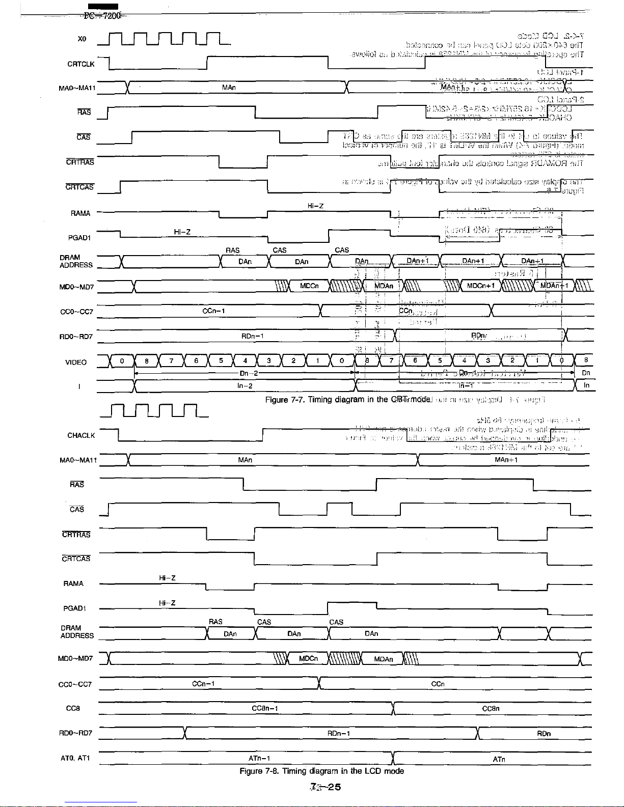
xo
,C)::s~~;
D':lJ
.£:<),D\'
:nl:::::!r:"cn
');j
T;:)
I-l.
::,_~
~
:,;j.1
::.1
j~j
dB
'.J).;:<l
8rl1
CRTCLK
I
L
_______
--'
'~V!OI;'O!
2.,
b )
;-;j~:
):.'-1'
,Yo
',"
I~".-"
.-:..,' , \
""""',' ,--.;
'~'JT~'
]-],-)0 ·xlT
(_~~;j
hn:i'-1- t
CAS
----'
"lSi?
'!Slq;olo
~1'-1
L-
__________
-"'"""'..w,
:::llU!:.lI--;
Hi-Z
RAS
CAS
rC",A",S,---=,-_,r
___
~r
____
...,r-
____
_
~~~~ESS
~--------·X'-"':::D:-A-n-'X,-_.::D:.:An",---,X
~f,i-;-:X
D,An£1
-X
iDAn+'-"'~,j",;~A~i'l
F
MDO-MD7
__
..JX'__
_________
-1ill\\\~'___M_DC_n_~
... ' ..:,;M:::;ciA::::n-+,'i'l0.,'0,\
\\\\~
MDCn+1
~"MbAnt1
~
_______
-=---,--
_____
----.~---',.""'
IL,;,,-+--"!,",,,,'
''''''-'''''.;=1''''''' : __
~
, I
CCO-CC7
_________
-=c=Cn~-~1~
_______
_AX
__
~,~!,~i~_~p~'C2r~:~,,~,-~,4,'------iXL------+'---
] I
RDO-RD?
______________
~R~D~n-_'~
________
..
~
__
o~~---~--~R~;PQr~1
-~,~"~,-~--_t;x=====
VIDEO
CHACLK
B
__
..JXL
_______
~ln~-~2
_____________
__iX~
_____
~_"-
________
".::ln~~T~-
___________
~~
JULJ1SL
,'-------------'
Figure
7-7.
Timing
diagram
in
the ClBlirmdtfa!
').11
nI
'i';,
'f:3:'_F':U
'11';;:'-]
,
'I':i
~
:.;~]!~
dd
'-,~"n:llj:'
1j)
-,r
__
;
'~'-I)l'lll:
jJ'~,-"1
),-"
:'-;c,d.""
[)-1".-;i[;.<)
";
")'
I:
..
: ... ;,
i~l
,:_)f;t,':i~'",.",:,·,
,1,"1
11, ,-,]'
)\/'
~,
:Jill!
'~I"';'-'_'-~
)
J1
i!; ) ;-)
I
'~
;
MAO-MA"=====X~
________________
~M=A~n~
__________________________
~X~
__________
~M~A=n=+='
____________
_
J
'---_-'11'---_-'
L
Hi-Z
RAMA
PGADi
Hi-Z
I
RAS
CAS CAS
DRAM
X X X
X X
ADDRESS
DAn
DAn DAn
MDO-MD7
~
~\'Y-,
MOen
~
MOAn
~\\~
'C
CCO-CC7
CCn-1
X
CCn
cca
CCBn-1
X
CCBn
RDO-RD7
X
RDn-1
X
RDn
ATO,
ATi ATn-1
X
ATn
Figure
7~8.
Timing
diagram
in
the
LCD
mode
,:Z:;~25
Page 75

xo
MEMW
CRTClK
IL
______
---I
CRTCAS
_____
....J
XO
MEMW
CPMES
CRTClK
IL
______
---l
CAS
.IlL
__
_
CATRAS
CRTCAS
_____
-....l
CPURAS
CPUCAS
DRAM
ADDRESS
CPURAS X CPUCAS
XL
___
JlX
L
__
r-
___
~CPU
WRITE DATA
MDO-MD7
~
>----
XACK
Figure
7-9. Video
RAM
access
by
the CPU
in
the
CRT mode (Write)
L--
__
IlL_----.J
DRAM
--y
ADDRESS ---11 CPURAS
X\._C:::!P:..:U~RA~S'-.JXL
__
_
MDO-MD7
___
~lli.I;~\\V.L_~
CPU
READ
DATA
XCACK
Figure 7-10. Video RAM access by the CPU
in
the CRT mode (Read)
7-26
-
PC-720D
Page 76

xo
j...,~~_~,"",-r_-_-_-_~_-_·
__
-_-_·
________
...J'
'mnli,
6PMESu-------,----------------------~
",",
-~-"-.,
...
-~----
•..
--
---_._-
_.'-
,
_~J
CHACLK
RAS
I
----------
--
---_.
.
_LI
_--'-
__
--'-_----1_
L-_---_--~_---'-.
__
--LI.
u.
____
••
_J
CPURAS
-----
----u,r--------------,----;---------,
L___
_ _ i '--_----'
I
xo
,\
j\~'
-,QRAM
,,-;,·,,C-·,-----.,X
CPU
X
-"'uu'AODRESST".
RAS
-I
1
CPUCAS
XL
___
-'X
L
__
_
.
':
-, j _ , ,·s:
)-1.
~
_____
~-'"
CPU WRITE DATA
MEl.OmMO?
:
----'>---<
}---
XACI,{-,"I."
Cigur~
7-11. Yideq RAiI'I_1"'cess by the CPI1 in the,
lCD
mode
(Write)
._'
••
-"
".
,_, " ".,1
,-,,:,
,
',r,)},
I'i,.
r:
'_"-:;"!
_'-\
:"IU'-~
L-
___
~
___________
-_·-_-...JI-
71))""
CPMES~-~--~~----------------~---------------------------------------------------------
CHACLK
1
_______
.1
C¥u
__
h
_ J
.
_,_J
.J
L----'----'nL,---_u-
-'--
__
-=-
____
:---
-L,-I
-+------'
,
-eRTRAS
L-Lr _--_-
---11-
-u
-1'--
__
--+-
__
----'
u CPURAS
------
--+
--
·CPUGAS--n--
-1--
u -f ---,
\
-.
_.-
--,-,0
)1:-
•. -
"
,I
1\.
1,.",-1
;,',_JH
i
I'l,~'
____
ul
,_u
___ . ___ . ___
_
!?~AM.
ADDRESS
-.:,:;-j~:,
ji
~,'\
1;.}
~g~-MD7
XACK
'1,
'I
1
CPURAS
X"---,C,-P::::UC=.A=S_OX
_
_______
..JX'-
____ _
\\\IX
CPU WRITE DATA
Page 77

xo
RESET
CHACLK
CATCLK
PGAD1
AAMA
XO
RESET
~
CHACLK
=
CAS
CRTRAS
CRTCAS
CPUAAS
CPUCAS
PGAD1
RAMA
! i
, ,
j I
I I
j I
I I
I
I
,
,
II
I
, ,
I
I
,
,
I
I
,
j
j
I
1
I
I
I
I
,
I
! I
H
'--_-lnl-_---'
Hi-Z
If
the
CHACLK
falls
in
this
period,
each
signal
outputs
as
above.
Figure 7-13. Reset sequence
in
the
CRT
mode
'--_---'/1'-_-----'
Hi-Z
Hi-Z
If
the
CHACLK
faUs
in
this
period,
each
signal
outputs
as
above.
Figure
7-14.
Reset
sequence
in
the
LCD
mode
7-28
-
PC-7200
'--_---'111-_--',
L
Page 78

'"
"'
~
..
---:---
--,
: i
!
'-----
r
-:c
..
-
----
J
·---l--I·
1-
1
I I
:-~-=-
._--._
..
_1
---J
L .. _
..
,
_J'--~
.1-
----t--;
...
---
.-
--
-,
L
_.
_ ...
__
J
r----
j I '
~+--
·fl
...
----"' 'ItL::lt .
____
~r
;0-:;;'-"""--'
--.=,-
-
..
-.
'1_
..
_
__
~:
i
-"-1-+--:--'"
-'-
w
-
•
iii
-
~-
-
"'-"'ffi¢
-
~2
-
1lIc;il::c9
'"
~r~'
~i
!g'l~:
~~r;:::::::J!",J~'-d"
dJ··
..
-j--~
..
------.
---~~~~'"
._----
',---'
" .
f---
-
"),Yliil
-r
f---
-
-
-
H
·,1'
',c',
,,:<)
':)(B
;-;!f:)IL
;J,:'
h'
j.-"
),!
•
'"
:1:
29
\
~11;
J'.
~
~---~-------l-
..
._-
:
,-
,.1
1
L L
1
___
,
,-"1
.'
-lrl
L
i i
, , ,
I'
lH
+
l
'r
,
:H
Ii
I
N
I)X
w
("'I:
u
1'_:;','
Page 79

....
I
Col
o
A
B c D
7-8. 5C4752
(51-2
1/0 CONTROLLER BLOCK DIAGRAM)
6.
'"
I
co.
,
co,
C
U
I II I I
'----,--
m
..
,
5'
"'
-
I I
IIII
II I
-
0
tt,t
llUU
U1U
-
~
-
,-
Ig~E~
C
{>
f--
8259A
1I25!1A
0765
[PICl [PICI
~
4
~
~
r-
n I
Inlll1
3
II II \ IIII
I
,-
l~b~~!f:
01
PARITT
"
IOCIlCK
CLOCK
SELECT
!IliON
80281
21
~E5El211
,
60512861
•
CDIilROLL
NPC51!
1 1
oUSTN
ERftORH
NIII
PCIOI
IIlCHCKH
eLK
elK
YFO
~
19"
1611
elK
TO/FROM
FD
AND
YfO
tAD-FeZ5:;
A B
c D
I I
II I
11H
112S(
I I I 1
II
I
'[
"
E
F
G
I
II I I
J1,1
1 1 H
11250
I'ARALLEL
STUUS
DECODE
...
'"
COHlfttlLl
lOGICS
-
n 1
IIn1
11111
[ I
II
I
y~1
; 1
DISI'
TlIIE
'"'
DISI'
<CO
E
-
-
-
SERUL
IISo KBClII
CEN1RDN1X
110
INlERFACE
F
l
'"
fRMIE
SIGNAL
GEH.
G
H
H
5 CHIEN
I'
CHIEN
IIHN
HLDA
6818RII
68111AS
681805
RAM
OS
""
6
5
8042
CS
I
14
~
~~~~NI
(SHDHON
CSCOll!
RESH
REFRESH
OREU2
FRMAC
fRHACD
3
2
n
o
Page 80

,",
,qJ
II
::t
6
5
4
3
.2
,Ii
"
A
B
c
PC'7200 INTERCONNECTION DIAGRAM
'I
•
",~,
•
L'
,
e'."
Uf,:
..
"
L~b")'
I.:"
'-Q
L--.J
II
Jc.
>J8[
"
,
KEf:
BQARD
. I
, I
---+--,
"
D
"
P'ANEL
E
.,.
"
7
___
- - ---1--
---
--;-1
, ; 1
'1
I
I
I
!'
LCD
'UNI
I
f
'I'"L"O.
w-
I , I
I , •
, I i
!-i
r
I .
I
~,I
:-L",,-
I
'·"·~j
. ,
---·'---1
i,
--~--~
'";
'~,.
I :
~~~,
_._,
_~J
L.
".
·IL··§f·.·.:.
'l'Ef:
~-""P-"
i .
~
II'
I ;
1'1
1
::-:-
'..
i
;·i
+--->
.
. "
"
....
,
I'
I
E!
,G
o
'HI
:::t:
..
?i;
~I
;{;;:~:;i:;-~
6nll
:l!l
::0
." .
!»
'-Ill
.r--+-"L,I!;:,t,,-1';;"lll-~
j-
~",,,
,n
Q
::0
o
c:
::j,
,
--W--
15,·1.1;;""
j
~
PIS
II(lARD
",
UNIT
,
___ ~ Dlh
~t'
rc
sw
,I:
5»
I
Z·
o
;g
::0
i:E]
I
.'"
..
'.
If
; ,
-II
... " 1-'"
I . '
1$1
""",-I_L
I •
I!
.'
II,
' I
1,-
lin.
'[.it
~
"tI
40
il
en
,~,
"~u
tEO
BOARD
-'i
,
i
.+
, I
I
--
,
'r
._,
'.>.,j~
I'
_
<-',
I
.Jl '
'.
"-,
L'-
[!.-
_'J
U i
~-,,-
r--------,
, I
, I
I I
I I
I I
,I
.__
I
Ii
..
;;\
l,
I
HODEII
l--'
'I
BOARD
I
~
I
Ii
:
__
CE~!Q}I__
-l~
I i
I 'rrTiloHl I I;
I 1 I I I
\_'---_
i
_\~~
illl!
j
.Il .__
.1
Lrt-l-r:iPj_1
-,
-1r-LJ---!:.Fu-
UNE- -··PIIONE-
PC-72~1
FD~l
PC-1Z02
FD-l.
FD-2
~
PC-7221 _ FIl-l •
HD • HD
CON1ROLLER
'"
3~P
'"
-EXPAHSlAL-
t;D~ti:;S6
;:;C0~,?,~
("3~~:)
~\(p
~~~;(\lUJ,H-jcri-
-":'~J
;'::';j
\)
__
,;(
D!~
',-,r!:!
I
A
'
8
c
I1AIN
IIOARD
~IO,
PRINTER
",
D
'"
~.
~
SLDT
((61
E
""'*
! 1-
,
Ii
r
~"
'"
..",._ CDNl!!!.lLER
IP:C-1Z211
,
~
."
SLDT
(81
F
'I'''';;
"""
•.
J
1""""1
1 1
noy
ONLT!
: ,.!,
~!...I
h'
I
J
!;-..
.1
1.1
G
-
H:d)
,
i-'-rC:c~~'~,.
",'
"'"
_f~
D~.!V_~.~I~:,I,",,:
• J _
'\
~"
,--_!
..
~\',
L
,~r-.
:1;.
-T--
-,
'IC,I!
FII
DR1VE
UNn-2
--'(PC-,~;;r':=-:~
~:I
",
HD
DRIVE
UN1'l
(PC-n21)
'fj
~:
Zl
ITO
~
::0
..
,3»
is:
, 2
i
I
Ie
,
,
,
I
Id
'
I
,
,
Page 81

-
-
-
-
w
-
-
u
-
III
« t,)
:::>
II.
t,)
I
."
1
I
I
m
1
N
."
1~!i~!i!i!;!~I~:;c=<~:~~:n~~:~~~~~:;s~~~~~~
~ ~
B
t+1-H'-H-I-I--H_~
~~
r
-
'1
••
•
iii
~:
llHi
!l!
~
*
!!!
~
I
B-2
1
N
1
I~
5
:;
•
•
"
"
1
-
PC-7200
'"
I~
§
;;
•
,
"
"
"
<
3
::c
w
-
-
u
-
f-
«
Page 82

----~~
, '
LL.::
w
Q
u
>'
~
c::
liJ
!¥i
ii
~,
1""
::J
~a;J
~
-
,,¢-,;
.'
i
. '
.
:,'
.
. "
~icL~~o
,; '.,"(;'f
,,-,
1.-
, .
-
•
,\,
Ln:
..
)
i
"'1:
'I
I'
.
----.
cn::-.
,.)
C\r!..:
,;
,-."
--~-!
!,
~
,~;
I,
'"
·'1
1_,.
.....
~"4
H~
:~~
i i
I
j;'
~
:~:--:
••
! :
: ,
I :
'-.J
I.,
Iii,
~I~::'~:'
_,~~i~~
~
t~~~J':~
~
~
~!{~
~~.':~
~:::
~~~:~~},~
~
~
~
-----"::"'j
w
u
Page 83

-
:r:
-
-
-
w
-
-
u
-
I-
:::l
(,)
a::
(,)
:21
c(
""
a::
I
•
1----
•
••
• N
I
~
XOI'
XD6
XCI
~
XDS
XD12
XOII
~P\~
'"'
'"'
'"'
'"'
'"'
'""
I
,
~~
N_
"'g~:;;
~!:;::;
':;l:
;;:1~151~1~
= , , -• " • •
.1'
-1=
I:-l
XDIS
XD?
r-::
:i
~XD14
nXD1~
nXD12
b
N
iil
E-l
X010
r~'=
'" '"
~
.,
<ilL:: "';::: "'.,-=:: "';:
,.l{~
-;
,..
'"
-;;
tv
ell
:;
...
I
i~,-,
1/\
l\IAi/\
..
02
AIAIIAI'\II\C
'j"\,
!!l!!l
I
::!
~
XDI
r-::
~'i9
"''';=
~
~ ~ ~
,
•
I
6-4
I
'"'
'""
'"'
'"'
'"
'"
'"'
••
Nrf
~.~I"'
.~
.-
~~
00
-
PC-7200
,
-r-~'~'~"c-~'r-------------------------i.~
~
~
-
-,
/
~:
"
- _ J
~
~
~
~
~
'"
••
f----------------~
'"
~-
I~:§
~~
•
xo~
_
'"
X02
~ ~
XOI
~ ~
'"'
I
I
-
-
u
-
Page 84

,'D,
_
0):
I:
:
, ,
,
"i
I
1
i!
0.',
w,
'"
-,
--'
(j
'10.
I
"-
«
00
~
'"
Lf)
.N
1"'"':-------,
I I
~<)~;
-
~'~~~~l-'
~"
I
.
_~:.
t~
_~
~
:
I I
L_
_
_I
"
: Ii
••
t-----""""
,-t-f-k
.'.
<
, '
;;:
'-'
~
N
u
OJ
--!
C
::.;]
, '
'_0
.'~-:'
;:.
:.1
«
~.~
llh
";-\
0'-
~,..!
Page 85

-
L'J
-
-
lZ_SAl
la-9AI
12_9111
16-3111.
16-9111
.....
W
(,Z-4111
16-3AI'"
12-'AI 16-9111_
IS-SCI
IB-SCI
16-1DI18-4111
-
=
}f3
-'"
~,
"'"
.'"
'"
19-4111
""
""
""-
[9-5"')
~
IS-SAl
-
'H"
[.
u
""-
§
,
•
,
I",
I",
I"
I",
1m
I",
,
'-"
'-"
"'-
,
, , ,
,
I--
w
.)
+[2-2111
l1-SAI
I--
(1-2AI
I--
Page 86

:r:
=
-
-
d
-
I-
o
!
,
:::.:i
_"L
1
~0
.
'.~';
I,:
"'-+~H
" " :
'.'1
I
I ,
"
,
'"
1
UJ'
1
I
en
['
,!.
Iii:
:tfll=
,c
:~
I"
I"
I"
'
I"
"
'lie
!'~
;,-
"
I'
I-
:r:
I-
(9-IAI
w
19-2AI
,
"
I-
fl-2HI
I-
u
I-
Page 87

-
-
-
w
-
-
u
-
...I
o
0::
I-
-~
t)
)0-
ct
«...I
0-
W
o
•
,
,
;0
•
I
I
;;
~
"
~
0;
~
@
•
~
g
~
~
;
;;
,
=:::c~~:~~~
...
'"
- :::
~I
'"
"'-
~
•
~
;;
•
;
~
5 5
~
•
, ,
I:r
•
E
. -
,
"
"
-
;;
:;;
• •
• •
;;
<D
~
I
I
,
~t
'
,
,
'--
""
""
'""
""'
'"'
""'
""'
""'
""'
""'
~~~~I·IH'·
•
;;
• ;
'l
•
~
5
5 5
"
•
, ,
,
-12:
•
E
- .
'I"
"
,
"
• •
"
;;
;;
"
,
I
I
B-B
m
I
N
3
ij
~
,
~
;;
5
5
5
~
~
"
,
,
,I;
J
U~
-
"'~
-
E
;
.
'1
0 .
,
"
"I
"'-
~.~o
•
• •
,
•
~
•
. ,
"
"
5
"
5
5
I
N
PC-7200
I
r
-
-
,
0::
•
••
1.
~
~
'F-"==~
~
"
~
;;
;
~
•
5
•
, .
-
-
"
•
,
< <
5 5
5
5
oL~1ii
""F..---"i
""~,==::1
"'"~·t==~
DU:l
'"
ou~
..
""'
Po,t====~
Dul~
",r.'t:===t==~_J
CPl
~
~~
, '
'"
•
'"'
,
'"'
•
'"'
,
'"'
•
'"'
•
'"'
,
'"'
~
"
"
,
5
,
§
•
5
I
-
-
u
-
Page 88

____
1.0
.:_
_ ___
__
_
___
_ Ln
--
--~---~--
..
--
-
m'
N-'.
:r:
cd'
w
~
I I
,
~"'i'
'
'.
,-
";:',
"-;
,
, , ,
,
:
,
'.~
,:r.
I
"_,
,-
';'~,
,
'/
:
~,
"'-
,
'_,"
..
"'"'
m
Page 89

(J)
I
~
o
6
5
4
3
2
A B
c
LINE CONNECTION
::~
::~
..
"(II1_C3.(1I2_A,.0I4_A2,0I5_19
SOl SOl
II
CCNl_113.CN2_AII.CN4_BZ,CNS_20
S[)S
SD3
It
'IICN1_A3.CIIZ_A7.CN4_U.CN5_21
504
SD4 ~ CCN1-C2.CN2-A6.CN4-BS.CNS-22
5DS
5DS"
CClll-B2.CII2-AS.CK4-H,CH5-23
SD6
506"
fCN1-A2
.CN2-U
.014-64
.CNS-U
SD7
507
II
.CIII-(1
.CNZ-A3.CN4-AS .CN5-Z5
5011
soo"
CCIII-ot
.tNZ-At
.1:114_05
.015-26
SDlI
509"
«CIII-1:26 ,CMS-CI I .eN5-2.7
sOia
sOia"
fCN1_A27.CN3_CI2.CNS_2S
SOl
I 5011 .. «CIII-BZ7
,eN3-CIS
.(115-29
sm
5012:
~~::=~:!:~::=~:::~::=:~
(I-Sill
;:::
::::
~
~CK1_1!2e.CM3_C16.CNS_SZ
~(I15
~(I1S'
tClll_CZ8.CNJ_Cl,.CNS_33
$U
SAO
~
tCNl_AZ9.CM3_C1B.CII5_~4
SAl
SAl.
IClll-C18.CII2-A31
.CII4-A6
.CII5-9
SA2
H2 ~ 4Clll-B18
.CHZ-ASO
.CII4-B~
.CNS-l0
SA3 SA3
~
~Clll_All!.CN2_A29.CN4_Al.CIIS_l
I
su
SA4:
:~::=~:~:~:~=:~~:~::=:!:::=::
SA5
SA5.
ICN1_AI7.CII2_A26.CN4_BS.CNS_14
SA6
SAG
~:!
::~:
:~::=~:::~:~=~~~:~:~=:::~::=::
SA9
SA!!·
tCN1_AI6.CN2_AZ5.CN4_Al0.CII5_11
~::~
:::~:
:~::=~:~:~::=~:~.CN4-B1Q.CN5-1S
~
CCIII-Cl0
.CII2-A20
11-5111
5A12
5AI2.
IClll-Bl0.CHZ-A19
~A13
5A13
::::
:~:::
:~::=~~:~~:~~~~S
5A16
Sl\6'
tCN1-B9.CN2-A16
SAl'
SAl'"
ICN1-A!!.CN2-A15
•
tClll_CS.CIIZ_AU
5Ale
SAle.
ICN1-BS.CN2-l13
SAl!!
SAl!!.
ICNI-AB.CII2-AI2
•
~CNI-C22.CM3-Cl
[
~~::!
~::!.
tCN1-A2MIIHS
~~:~:
~:~:.
tClll-B22.CNJ-1
(1-3111
£LA21
tA21.
((III-A22.(1I3-1
Elm
lA2Z:
:~::=~::
:~::=~~
CAD-r026'
!~~:3
~:~:
•
ICNH21.CN3-
1
15-4111
Sr1Enii
5nEKR ~ CII3-819.CN2-
12-UI
•
Clll-C6.CH2-B"
12_4Al
~IIW
S~W
•
Clll_BE.CII2_Bll
iJii
~CN1_B1.CN2_1!14,CH4_AI2.CIIS_6
!2-5AI
..
12_5Al_
12-4111_
12-4111-
.CII5_B
16-IEI
16-601
""
Eiii
!1I06
IRQ,
111010
]RQ11
111012
111014
l!1UIS
lila,
......
,
l11U&
.1
lRQ7 C
IRau
.~~1-.2~
.C"3-D~
::::~
:~::=~;::~::=:~'CK5-37
IRQIS
"CN1-A2S.tw3-D5
1R09
fCNI-C4.CN2-04
""'[
12_3111
HEN
AEN ~ CNI_A6.CN2_All.CH4_AII,CNS_5
11-5HI
SOliE
S9HE
..
A
B
C
D
E
D
E
F
G
ORQZ ORQZ
DRQS
ORtiS
[
,~,
'""
IS-6f1
:::
~:~:
:~::=~:~
:~::=::~
ORQl
=
ICN1-A32.CII3-D15
[
rnKf
UACKO"
CH1_C29.CNS_DB
15-4111
16-5111
19-5EI
IS-SEI
(5-SKI
(1-1111
12-~lIl
~~",,--------"'f;;'>
12-9111
12_9HI
IS-&fl
IS-6FI
IS-6f)
14-1111
14-&1lI
1~-6HI
14-11l1
:~=:::
VEE VEE
;
16-lFl
~:~~CO
1\
"
16-6111
ICII~_B16
12-11l1 K60ClK
~
.CII12-1
12-1HI
IIBDOATA
~
ICN12_l
F
H
%
!AA-91
6
5
-611.1:115-'
4
3
2
11
1
g
G
H
Page 90

6
5
A
-I
- B}
c
D
CONNECTOR TABLE 1
;;.-c<
l~,
;.,
,:-<'.
\'
~
L-,Expansion
-YO'
Busl,'
-~l_
,
~J,
...j
'"
'''fI,
riO
N,:_'
,'signal
__
~-iO'
R~
,Ai
"
.>
I/-OCHCK-
<B1 -~ SD7:·
,I
c,
':1
n
"R~D2
Signal
A2
,SDS-
---
-82 -
SD41"'-c!c'"
'C2''-''-
uSD3
'A"5
SD2
,.
'B3--
SDl.----.l,:·"
',C3,-" LS»O
A4
GtiD.
B,4
RESETPRV
_
,C.4;,
Uill9
'AS.
DRIlZ -BS--DWS"
.~.:
'J
::C5
"'.
~I10CHRDY
·'A6
-AEN--
B6-
J
."
'C6: - ,
Y.~
'A7!OW
B7'
TIi'ir
.
.-rJ
-11
'C1'~·"
~'GlID
''';' " ..
"
--~-n
iAIS/"
~..
',C8.~'
·SA17.
Irs
",
"-"
..
"
I,
AID"
SAB -
B10--SAl2
,"
,clih
IISAll
-
Hi
SAlD-
BU
-I' DAm·-
"·en··
~DRQ3
~lZ,
1--DACKr
']1'2 DRlll-'"''
'ca2"~
'Rmmml
11.13
:,
eLK-
B13 -GND'
~'"
CH,,' jRQ7
I
Alt'
'UQ6,
Jll4
IRQ5,
, "
,elk
IRQ4
'""
',M
".
~'''"'_
,
__
,
SA7,' ,
BALE~
" ,I
:~~.",
,Al2'--
(CSl6,·
o
,
GND
'-j"SBHE
,
run
:
\"LAI8
,"IRQ12
t.:>'-,--L
U\IlJ.:>
Dl;;J
,
'GND
-n"l
'SDO
2,
I/O
Slot 1
A2
SD7
J
Signal
GND
RESE
A3
SD6
B,
1"'V
A4
SD5
B4
IRIl9
'5
SD4
BS
SV
6
SD3
B6
DRQ2
7
SD2
B7
12V
8
91
,",
10
l!OCHRDY
••
AEN
L
•
I
SA19
DU
SAl8
B13
n
....
"'.4
lOR
5
DACK3
6
DRIl3
SAH
B17
DAeR!
SA13
Bl8
DRQl
SA1Z
B19 I REFRESH
SAll
B20
eLI
SAIO
B21
IRI
SAg
B22
lRI
SA8
B23
IRl
SA7
B24
lRI
SA6
B25
IRQ3
SA5
B26
DACK2
" "
_SDlO'
,Cli"
.SDH.",
,
'i'e
1'Lt.1
.:1M
~
TiC
SDn,,~:,
C28,' ·,SDM,
B:)
A28
SA3
:828
I
.ALI
·C29·"·
mcxrr··~':
,
..
~
A29
SA2
B29
+SV
u--
DACKS+
'C3iJ"
\J)RQ~""J'~'2';
A30
SAl
B30
'11.1..11.1;1
JSj1
-DRQ6~-'~"
-
-C3r:"
A '
•.
:;~'~
A31
SAO
B31
TURQL
B32~,
,C31",;·,'.tEc'/.'·'.'L:"
ose
,
GND
~_,
i. " :11:-
,'_:
',,,,
- "
'L"
.,
l
"_1
'L"
1_.,'
-[112-
7.
LCD
':,,'CI,--
. " --
~'.
"C~'':''
in N
Signal
I,
N
Signal
~
-~
:
..
·.o·c<-
;1
[" -!:
". -'"
'c':" -;
~
"
1
GND
2 S
3
epl
4
CP2
~:
~.)-~',
•
,,!
".
~
i"
'-,,2
:,
',,"--.,;·u,_c-~.l
;"
,""
' ~ -
0:
I '
5
•
6
GND
7
---
8 +5V
-,--;".'-'-J,"'~'
'~'[c'i-"~-rli:'-~,"
9
GND
10
VEE
;'-'
:.](.
",
·.··f- ',' 'i.,."-:"
11
DUO
12
DUI
_". " "'l'-'
,',,~-~.
13
DU2
14
DU3
"'-",
..
,',<>
J.
15
GND
16
OLD
17
DLI
18
DL2
19
OL3
20
GNO
;'"~
-~-j
~~D-~
"jl:"
P:-\j',;,l;jf;-e
, ',,!,i'
A
B _
c
D
E-
~
'-
-
-,,'
G-
-~
a,
I/O
Slot 2
4, Modem
in N
Signal
in N
Signal
Al
GND
Bl
GNO
A2
SOD
B2
SOl
A3
SD2
B3
SD3
A4
S04
B4
S05
A5
SD6
B5
S07
AD
SAO
B
SAl
A7
SA2
B7
SA3
A8
SA{
R8
SA5
A9
SA6
B9
SA7
AID
SA8
BID
SA9
All
AEN
B11
RESETDRV
All
lOR
B12
lOW
,Al3
IRQ3
Bl3
lRQ4
A14
+5V
B14
+5V
A15
+12V
Bl5
12V
A16
GND
B16
MSPO
-
-6.--Floppy~nisk
_..;:
[>' ~ -
..
I ,
'r":,;
-
'"-t~J)
-..jC'"
'f';
't:.~'
""
E
F G
,
--H-
%
IAA-II0)
L~ \ --~J
~
~
"
]
"I
;6
1
~
'jl'
5
!"
4
3
2
i
I
!
c
I:
I--
I
]0
Page 91

(I)
I
I\)
6
5
4
3
2
A 8
CONNECTOR
TABLE2
tAI)-
A
B
c
8.
RSZ32C
in
N
SigpBl
1
GND
Z
SO
3
'0
•
'TS
5
CTS
,
DSR
,
GND
,
CD
9
---
10
---
11
"
J3
---
c
D
in
N
SigDal
U
15
-=
"
-=
17
-=
"
-=
19
----,
20
DTR
Z1
---
ZZ
er
Z3
---
U
=
Z5
~
12.
'Speaker
in
N~
Signal
5P
2
Vee
14.
Power
2
in
N
Signal
1
+SV
Z
+SV
3
GND
•
GND
,
GND
D
E
F
G
H
lAA-l11
9.
Printer
10.
CRT
6
in N
SigD1I1
in N
Signal
in N
Signal
in
It
Signal
1
STROB
14
AUTFDX
1
GND
,
1
Z
DO
15
ERROR
2
GND
,
VIDEO
3
Dr
!8
IlHT
3
,
a • me
•
DZ
17
SLCTIN
,
G
,
V
me
,
.,
18
ORO
, ,
,
..
19
GND
,
OS
ZO
ORO
a
os
Z1
GND
11.
LED
5
9
D7
ZZ
GND
10
AOK
Z3
ORO
in
N
Sig"al
11
BUSY
"
GND
r IBD
eLK
"
PE
Z5
ORO
2
KBD
DATA
J3
SLCT
3
+SV
•
STAND
BY
,
SELECT
A
13.
Power
1
,
SELECT
B
4
in
N
Signe.i
,
GND
a
LCD
CONT
1
OFF
,
LCD
RV
2
+12V
10
GND
3 +12V
•
l2V
,
5V
,
15V
,
ACL
a
GND
,
ORO
3
2
rl
8
E F G H
Page 92

LL
fi---~~
)
'~
-,
,
"
U
)1
-L
___
-----"__
_
(\J-;
,-
8."..
13
n,
---,,-,
-;=
,
cc
'--'
iLl
1..::_
w
I • I
.~
I
u
I ,
~L"
'",
"CI!
Page 93

PC-7200
MAIN P.W.B.
I
I
M4V02
•
•
ALS245
8-14
Page 94

PC-7200
8-15
.;
~
•
~
.
~
•
"0
~
•
•
•
::
~
•
c
~
0
•
~
~
•
c
::
0
~
•
~
•
· ,
~
,
L ,
.~
~
.
I!
~
•
:
~
•
c
•
...
iii
*
:x:
u.
"-J
u
..J
0
'"
It:
I-
Z
0
0
>-
lU
~
0
0
«
(II
!o-
I
0
Il.
'"
"'
r-----------------------;r-------,
I!
! I
!~~
! Z :
r~
a
5a~Q.
55!
: i X I
_I
'"
~~CQJ
~~
1
~
~
.~
~
I
U r
~
~
~
r I
I I
L_
_______ _ ______
+
______
+_.
__
J
"'
.rs.r
.l.r
JS.!
...
..
~
4
:ro
- - o'
I"
t:;
L _ -
..J~
r-(:'
~.
,,'"
: •
"1,
~~",~~ro~~
I
I
7~7~<t~~7
i~~iiiii
..
•
o
•
,,-"-La.
• N _
.
..
_I
~I
~I
I I
~
________________________________
~
____________________
____
...1
8-16
N
:x:
"-J
5
H-++++-I
Q
u
'"
N
Page 95

en
w
a:
w
en
g
.,..
l-
S
o
a:
(3
~
D..
D..
~
en
a:
w
~
D..
r-------
-
,
5A
125VAC
,
FI
XFI
r--------------1
,
"
on
r"'----1
I
I
_____
Jfl
------------------,
I
L2
I
--...,
I
II
..
I
I:
,I_I
C_6
___
~",--'
r --- - - - - -
---ir:::::l~lti~i
:---1 I I
r-
- -
---
-
---.~
..
--
r
--I-....,I
!
~
0'
I I
I
II
"':::
<D,
I I
,
I
C32A
R24
C33
-IH~tv-+
1-_-'I~,;",3.;.4_t-J:;:
C44
R40
R
L
_________
_
"'+-
"'
"
;.
"
'-
I
:'I!
rJ
~
~I
I I
I,
VRI
,L
J I
II'
Ilr-J
iil~
::
I
:"1
(-.,
ZD3
R:5
I
'~
I
L:J;-----
L!
~
1----1-1=---1--'11
C=O
R23
<31
z
"
n
~
8-27
.
m
'-
,.
'"
r
-,
0'
u"
u.,
,
L
__
-'
Il1l
Clg
+
R14
CISA
C17+
R31
o
~
~n
z
,,,
~
PC-7200
POWR SUPPLY P.W.B. 100V SERIES
Z
'-
0
,
'"
III
D
8-28
Page 96

III
W
it
w
III
~
~
l-
S
o
II:
o
>
...J
11.
11.
:l
III
II:
W
~
11.
r------------,
1
I;:.
I·
,
I
L
_______
.:._
r--------
Rill
,lyJ
..
u
1'"
I
I
I
1
PQWR:,SUPPlV.P;W.B.
20PV
SERIE~
~
, . '-- .
2
L
o
,
.",
m
'"
I'
,
~,I
El
8;-30
;,
,
Page 97

PC7202/7221 PARTS
LIST
1
Exteriors
2
Main
frame unit
3
Packing material
& Accessories· CE720K
4
Key
exteriors • CE720K
5
Keyboard
unit·
CE720K
6
LED
PWB
unit
7
Key
PWB
unit
8
Main
PWB
unit
9
Valiable resistor
PWB
unit
10 Power supply unit - - -
100V
series
11
Power supply unit - - - 200V series
12 Hard disk interface
PWB
unit -- - PC7221 only
DESTINATION TABLE
U
USA
KD
Denmark
y
CANADA
KE
Netherland, Austria
G
EUROPE
KF
France
H
U.
Kingdom
KG
W Germany
a
Australia
Ki
Italy
TJ
Korea,
Venezuela
KN
Norway
T
TSC
Taiwan
KS
Sweden, Finland
EH
Malaysia; Singapore
Ea
New
Zealand
KW
Switzerland
(E)
ESB
Saudi Arabia
KX
Switzerland (F)
Indonesia, Thailand, Philippine
E
ESG
Lebanon, Jorday, W-Africa
Hong
Kong
Pakistan, Argentine
ESGI
Iraq, U.A.E.
Please note
that
some of components were replace
by
new types, which are marked with an asterisk (
*).
While the parts
code
of
the new
type
is
given in Parts List,
the
parts code of the old type
is
not. Since
the
old
types
were used up
to
the
301
st
production unit whose machine serial numbers are listed below,
all
those three
components
marked
with
an asterisk
must be replaced
by
the old types altogether, even if only a component needs
to
be
replaced.
79101263 - 79101353
10
sets
79100013 - 79100203
20
sets
79108395 - 79108845
46 sets
79110405
-79111315
92 sets
79109355 - 79110395
105
sets
79101665 - 79101785
13 sets
79101365
-79101505
15 sets
TTL
301 sets
Parts marked with
".&"
is
important for maintaining the safety
of
the set.
Be
sure
to
replace these parts with specified
ones for maintaining the safety and performance
of
the
set.
Page 98

m::Exteri·Ors·:::;
.:,;,
(,
.-;
,)'j.,
~,'"
..
","
"'."'
.J:J\'J
"-"-,,,
n
"-'
·i;,."
.,,;,
"'-'''
s'].,)i']
OJ
Exteriors
.,,'
-
-,
•
•
*
•
*
*
*
*
*
•
NO:
1
2
3
4
5
6
7
B
9
10
11
12
13
14
15
16
17
IB
19
20
21
22
23
24
25
26
27
28
29
30
31
32
33
34
35
36
37
3B
39
40
41
42
43
44
46
47
51
61
62
63
64
65
66
67
68
69
70
71
,
..••
PARTS
CODE'
.oj.
'CCA'B Ai-o'o'pic
ir':!""
CCABA1047ACll
CCABA1047AC03
CCABA1047AC12
PFi
LWIOO3ACSB
PF i LWI
003ACZZ
PFilWIOO3ACSA
HPNLC2140HCSA
HPNLC2140HCZZ
GLEGG1024CCZZ
lPiNS2032HCZZ
MSPRC2025HCZZ
CPLTP2060HC04
CPLTP2060HC02
JKNBZIB76CCSA
J K N B Z 1 B 7 6
CC
01
XBBSC30P06000
LX
BZ1159GCZZ
ML
E VP
104
4CCSA
MLEVP1044GCOl
MSPRC2029HCZZ
LANGF
15 3 OCCZZ
XCPSD26P06000
MSPRC2030HCZZ
PTME
2001HCZZ
PBAR
2011HCZZ
LSTPP2004HCZZ
JBTN
204BHCSC
JBTN
204BHCSB
PBAR
1001ACZZ
MSPRC2024HCZZ
GCASP1007ACSA
GCASPI007ACZZ
XBBSD30P06000
LPiNS2031HCZZ
GFTAU1040ACZZ
GFTAUI040ACSA
XBBSD30P05000
GLEGG1009HCSA
GLEGGI009HGZZ
G LEG
PI
0 0 9
AG
Z Z
'X'B
PSD
40
PO
B'KS
0
MLEVP2023HCSI
MLEVP2023HCZl
LPiNS2030HCZZ
MLEVP2024HCSl
MLEVP2024HCZl
JHNDP2004HCSA
JHNDP2004HCZZ
CFRM
1005AC02
CFRM
1005ACOI
GFTAZ2030HGZZ
GGOVHI026ACZZ
LBSHC5020BCZZ
LANGTl124ACZZ
GCOVH1032ACZZ
PSPAZ2037HCZZ
PZETZ1026ACZZ
CCABBI041AC40
CCABB1041AC41
CCABB1041AC42
CCABB1041AC50
GFTAZ1034ACZZ
TLABZ1275ACSA
XBTSC40P06000
LX
BZ2058HCZZ
PZETZ1024ACZZ
DUNT
1790ACZZ
DUNT
17B6ACZZ
MLOK
1004ACZZ
LX
BZ2055HCZZ
MSPRC2027HCZZ
MSPRD202BHCZZ
LANGT2302HCZC
XBSSD40P06000
LANGQ2349HCZZ
QSW
M2043HGZZ
QCNW
1219ACZZ
XBPSD20POBOOO
LANGG2301HCZZ
PRieS
NEW
R[lNK
MARK
,
st'
,
'N'
B·Z·,
N-
'
BZ
N
BZ
N
AL
N
AL
N
AL
N
AV
N
AP
AA
AC
AA
AM
N
AH
AB
N
AB
AA
AA
AB
N
AB
AC
AC
AA
AC
AC
AL
AC
AE
N
AG
N
AC
N
AA
AC
N
AC
N
AA
AD
AY
N
AY
N
AA
N
AB
N
AC
AC
N
'iA'A
AF
N
AF
N
AH
AF
N
AF
N
AY
N
AY
AV
N
AW
N
AF
AG
N
AB
AC
N
AD
N
AE
AC
N
BG
N
BE
N
BE
N
BE
N
AL
N
AB
N
AA
AA
AD
N
CV
N
CV
N
AD
N
AB
AA
AA
AQ
AA
AD
AL
AC
N
AA
AD
PART
.'
..
d "
'.,
J.
.
"""D'Es
t~1
PT'I
ON
.RANK
-
__
'I
, '
E Front h6usiil'
uriit"
Nli2:....;;24
26.....:.40
-~
~
,
-
~,.
E
Front housing,
unit
(No.Q;.,;.24,26,--4Q)
-'-
.
'Of,
E Front
housim~
unit (No.2--24
26-40)
E Front housing unit
(No.2
.........
24
26--40l
C
LED
filter
C
LED
filter
C
LED
filter
D
Front panel
D Front panel
C Rubber foot
,
_
L;:_'
':
"
:'
'-'
_J-~-
,
C
Ke-
cable
in
G
Ke
cable s rin
-;
C'
Kev
cable plate
~
.J
".
>
~-
--
"
G.,
Kev cable pIa Ie
,
,
',",'
.. -.'
.. ,:~, .
C"
Cabinet lock button' .
,',;
,
C.
Cabinet lock button·. -
C"
Screw
3X6)
»
> ,
C
Screw
--
c;,'
Cabinet lock lever
' ,
;
<>-'
l
C Cabinet lock
lever.
..
c_
_.\
Cabinet lock...wrin·
_1
C Lock lever
an
Ie
C:,;>
Screw
2_6X6)
,
.'
"
;
".'J.
,
C Cabinet lock
sprin.e!"
2
C
LCD rutch pawl
C,
Push:button
bar,
C Push bar stopper
D
Push button
D Push button
C Push bar
C Push button
sprin&..
G
Button case
C Button case
C
Screw
3X6
G
Push button
pin
C Bottom housine
G
BoUom housinR
G
Screw
3X5
C Rubber foot
C
Rubber
foot
C Rubber foot
C
:Screwl
4X8K"S
i'·'
G Handle fixin lever L
C Handle fixin
le,jer L
C
Pin for handle
C Handle fixin lever R
C Handle fixine lever R
C Handle
C Handle
E Frame B unit
No.934
37)
E
Frame B unit
1fo.9,34
.......
37)
C Connector Cover
C Connector food
C
PWB
uide bushin
C Guide rail
anJlle
0
Blank cover
G Spacer A
C Insulator sheet 2
E Rear housing unit No.4,2742
44
E Rear housing unit
No.4
27
42
44
E
Rear housing unit No.4,27,42--44
E Rear housing unit
No.4,27,42
44
C
Box
cover
G Modem label
C
Screw
4X6)
C
ScreW
G Housine insulator sheet 1
E
LCD
unit
E
LCD unit
C LCD lock
C Screw
C
LCD spring
C LCD s rinK,R
C
LCD
allgle
C Screw
4X8
C Microswitch fixin
an
Ie
B
Microswitch
C Microswitch cable
C
Screw
C
LCD
damper
an!:!"le
-1-
,
! -~ ,
-,:~-
'J -i
.'-'
-[0
;~
-"):)
NO.
",-.
-
,
~
-.
-
- ,
,.~
.
UY
PC'7Z02
72
_ ottiehcauntries)(PC..,
7202
73
(U
Yl(PC
7221
74
(other countries)(PC
7221
75
(U
Y)(PC
7202
76
(Other cQuntries)(PC
7202
PC
7221
n
(U
Y
LOther
countries
78
79
80
(UY
(Other countries
(U
Y
(Other countries
,l,UY
Other countries
(U
Y
(Other countries
UY
Other countries
CUY
(Other countries
(Other countries
U
Y)(PC
7202
U
Y)(PC
7221
.,~
UY
··"tOther 'countries
(U,
(Other countries
(U
Y
(Other countries
(U
Y
lather
countries
U,Y
cr
J anI
(TSC anI
GH
E
CUY
(G
H,
,E)(PC
7221
(U only)
(Other countries
PARTS
CODE
PRICE
NEW
PART
DESCRIPTION
RANK
MARK
RANK
PDMP.,Q,1
00
lACZZ
AE
C
Dam
er
XBPSD20P04000
AA
C
Screw
2x4
CPWBF1115ACOI
AD
N E
LEO
PWB
unit
QCNW
1191ACZZ
AH
N C
LED
cable
XUBSD30POBOOO
AA
C
Screw
(3X8
CPWBFll16AC03
AE
N E
Valiable resistor
PWB
unit·
CPWBF
1116ACO
2
AE
N
E
Valiable resistor PWB
unit'
, j
,
--'<,
CPWBF1116ACOI
AE
N E
Valiable resistor PWB unit
QCNW
1196ACZZ
AE
N
C
INV.
VR
cable
QCNW
1236ACSA
AL
N
C
Key Jnterface cable + Core
QCNW
1197ACZZ
AL
C
Key_cable
LANGT2309HCZA
AC
N
C
Ke
connector
an
Ie
.----
-
--
- -
--
- -
-----------------------
--.
, ,
I
,
I
: I I
L
________
J
r---------=-
-----
______
,
";
':~,~1
,
L
__
-2-
51
- ,
,--,
' '
, .
"
"I
r
,J;':""
....
'.J
.J
,,'
"
-!.
"
"
;;
..
;.
. -
"
"
...
.-
.-.
'j:.I.
,_'.J
"
..
-",.,'.
I
I
,
I
I
,I:
I
)
_(U
onlv)
"J,;'J;].~
'l(y
only)
Other countries
-.
"-
<-,
.,
;,././,
,l,U.Y
Other countries
:""
:
'J
,
"
';
..
)'
"
Page 99

~
ill Main frame u 't
NO
,nl
, PARTS
CODE
1
1 I A I
'R:'ii~
I
~i:K
I
~ffi
, 0
;N
I-
H
II
NI
'CC
13
l-
I-
-
D
.J'
21
22
2
,-
28
~
30
31
32
lP
33
34
-D
35
p
4;
n
43
lPN
44
w-
-
45
q
46
A
4f
A
Jc::
:z
'7\
56
C
37
58
A
AC
A
:-ji
.u.
IHe
!H
I Q
,K
K
A
A
;-0
..
A
A
B N
A
A
N
N
N
[-
I
I
I I
I[ (
I
I
~
I
OV
I
!...!!!
,~i
~
~OV
I
'8)
3
'~
;-:
PC7200
DESCRIFTfON
fIiVi
(G
nM
i
-
-
;-~
(PC
=722l)
-
--j
-
PC7200
[2J
M '
am
frame unit
-
Page 100

...
=.===============~===,PI}Z.200==
..
~====~~"~",=,,,=-
'=-~"'=-'PC7"'20""0"F='""~======================
rn:J
Packing material & Accessories· CE720K
,
...
)
,.'
NO,
PARTS
CODE
I
~
i~ I ~:FfK • ~~~~
5
N
N
N
."
..
..
DESCRIPTION
....
i i
!forkev
Packin.
cushion B fRiehtl
, A (Left!
, case
'ac
n.
case
,
case
'ac ng
case
.
:PU vinvl
bas
CD
fixin.
i
linvl bee rI60X: 60..,
i
'manual
for'
yt
: :
, ,
'manual
for'
~-BASIC
:
cor<
.
'£H
(ExceDt Gl
(U.~
7'1:
on
IA
f-
A
:
F·
N
N-
N
!!.
~~~~~~-+~~~+-~~;~:;'=============--~~
12
:ev
c,
,Ie
J
13
14
15
16
.
17
.
18
19
62
63
64
IIO
-"
203
204
I
205
,-
'=
"-
'-
:P
z
A
B!
,e
A
,W
A
,W
3AC
Z
AW
N '
N
, N
N
N
:ev
"e
,plate·
I
~i
I i
linder
uni
i N.
:-
I Binder unl nclu
es
linder uni
inclue
es
linder' i nclue
es
No-
: cord I.eve
.
sleeve
er case
!er
add
, !
:inder
.ev
cable
manua
manua! for
MS-DOS
manual for
MS-DOS
ey
ten plate
~e
~media
N 'ummev
Dackin
for
inst
book
caSE
'or
'er
uni
i
es
er uni i
es
er un' i
(E,ceD'
,,V.
,,V.
(Exce,
mv.H~
IH(g~
U.ESBI
u:I
IG
onlvl
j j
(I
'Iv)
N
N
N
eN
N
,
:
case
manual for
GW-BASIC
invl
bee,
manual for key
I
disket
'er
case
Inder
'Binder
Binder
add
manua
manua
-5-
(G.i<WI
I onlvl
(EJ
(F./
G./
!
rn:J
Packingmat(3rial &
Accessories
·CE7?OK
''',
/!
5
CE720K
113
-
1~5'
-
13
q
c;J
'19'
( -
, , ,
~/
:
/~"''''''''~'
~-
:
,,/
?"
,
-'
,
-'
,
-'
-'~'GONLY
4
109
I~
112
-6-
101
102
103
 Loading...