

-
PC-4741
SHARP
SERVICE
MANUAL
CODE: OOZPC4741SM-E
PERSONAL COMPUTER
PC-4741
PC-4721
MODEL PC-4702
;------------
CONTENTS
-------------..
CHAPTER
1.
OVERVIEW
.....................................
1
CHAPTER 2. GENERAL
INFORMATION
.........................
3
CHAPTER 3. MAIN
BOARD OPERATION
.........................
7
CHAPTER 4. LCD UNIT
......................................
23
CHAPTER
5.
POWER SUPPLY CIRCUIT
........................
25
CHAPTER
6.
HARD DISK
....................................
27
CHAPTER 7. FLOPPY DISK DRIVE
............................
31
CHAPTER
8.
SERVICE-MAN DIAGNOSTIC . . . . . . . . . . . . . . . . . . . .
..
33
CHAPTER 9. APPENDICES
...................................
47
CHAPTER 10. CIRCUIT DIAGRAM
& PARTS POSITION
............
66
SHARP CORPORATION
This
document
has
been
published
10
be
used
for
after
sales
service
only.
The
contents
are
subject
to
change
without
notice.
CHAPTER 1. OVERVIEW
1. Scope
This manual
is
covered for PC4702, PC4721, PC4741 CPU and hard
diskdriv9.
For
detailed
information
on
other
auxiliary
equipment
and
options
(list
following),
please
refer
to
the
separate
service
manuals
provided
for
each
devices.
CRT adaptor (CE-471A)
MFD unit (CE-452F)
EMS card (CE-471
B)
SID card (CE-451
B)
2.
Service method
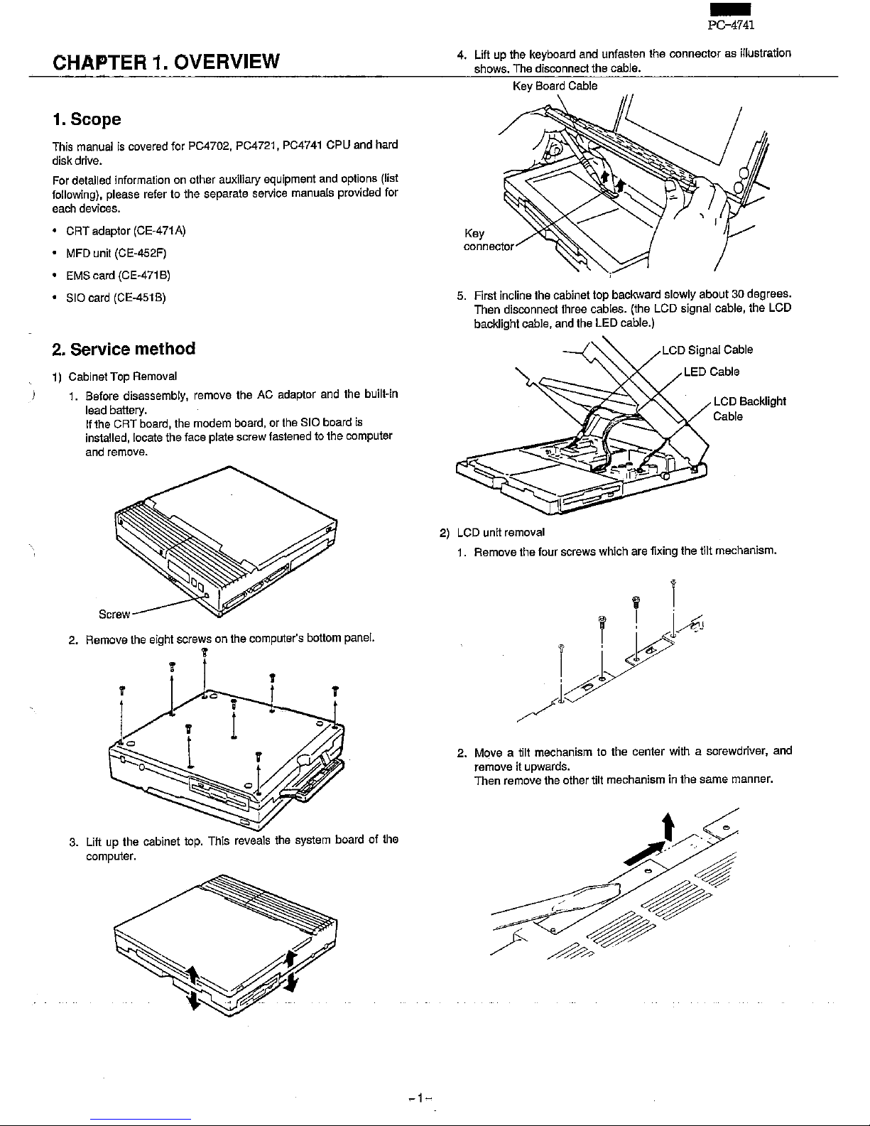
1)
Cabinet
Top
Removal
1.
Before
disassembly,
remove
the
AC
adaptor
and
the
built~in
lead battery.
If
the
CRT
board,
the
modem
board,
or
the
SIO
board
is
installed,
locate
the
face
plate
screw
fastened
to
the
computer
and
remove.
2.
Remove
the
eight
screws
on
the
computer's
bottom
panel.
'f
'"
3.
Lift
up
the
cabinet
top.
This
reveals
the
system
board
of
the
computer.
_1-
-
PC-4741
4.
Lift
up
the
keyboard
and
unfasten
the
connector
as
illustration
shows.
The
disconnect
the
cable.
Key Board Cable
Key
5.
First
incline
the
cabinet
top
backward
slowly
about
30
degrees.
Then disconnect three cables. (the LCD signal cable, the LCD
backlight cable, and the LED cable.)
2)
LCD
unit
removal
LCD Signal Cable
LED Cable
LCD Backlight
Cable
1.
Remove
the
four
screws
which
are
fixing
the
tilt
mechanism.
2.
Move a tilt
mechanism
to
the
center
with a screwdriver,
and
remove
it
upwards.
Then
remove
the
other
tilt
mechanism
in
the
same
manner.

-
PC=lfT4F
s
..
Operate th·" tCD.
r"leas~'leite"
'unfix;tns
;upper
cabinet and the
LCD section, and separate,
the upp-et:cafjinef:from';the LCD
section.
-~'.)
,,--
.'J
In
this
case,
be
careful naHa damage
tw~
LCD
cables.
Installation
1
..
,
Inst~1I
the upper,cabhlet
9n:d-1h~-lCD-,$e6ti,on
by
reversing the
.
,di5ass~mbly
proceq.LJre~:
'_,
_ :
_._~_
_ "
'When
installi~g
the)l~.mechanisrill·
~!3itl:1e_
-Shi~,tt
horizontally
in
. parallel
t?-
th~
ang~e
bott~m
and insert into the, LCD section.
2. Attach,
t~7'
l:Ipper and lower cabinets to the set.
3) LCD section
Disasse'mbly
<Caution>
For disassembly of
the
LCD
u,nit
j
1;18
su're-
to
.follow
the
procedure
below. If not, the cabinli:!lmay be damaged.
1. Remove the' keyboajd.
2. Separate the upper-cabinet
!rom
the lower cabinet.
3. Remove the upper cabinet.
4. Remove the four rubber cushions fixed with duplex tape on the
LCD. seqtion, and remove the four screws which were covered
by
the four rubbe(cushions.
-2-
5. Remove the fronfanci"r'ear-c.abihets
6f.the~LCD€fedti911.
-,
._
6. Remove the fixture which fixes the LCD section and the body.
7. Remove the reflection plate of the backlight.
S.
Remove the fixing screws and the connectors
otthe,
'.ilh)mil}~
tion control PWB and the backlight convertor PWB, and
. remoV" the PWB·s .
Assembly
1. Assemble the'
Lbb
urilt-
by
reversing
.the:
disa5's~mbly'
proce-
dure': ' .
..,
1 __ .
__
.",
Carefully check that there is no fingerprint on the LCD'secllon.
If there is, clean with a cloth and
a1cohQI.
:111e
cloth must,be
fine and smooth, such as glass wiper
dOt·~.
.. . '-,
...
2. Attach the upper cabinet to the set.
3. Attach the lower cabinet to the set.
4. Attach the keyboard to the set.
s.
HD
INTERFACE AND
HD
DRIVE
The HD drive unit can be replaced only in whole unit, but not
in
part. When they are diagnosed to
be~A~fe9ijve
bytfrediagi1qs-
tic program, replace the whole unit
of
them.
4) Cautions
1. Although the CE-471A CRT adaptor board is an
aption!ar
the
PC-4700,
it
pomes
standard for
the.
US version
pC4ipo.
For
more information about the
Wiring"
schematics and parts layout.
",ferto
th,,·CE471A
Service ManUal. '
2. Cosmetic sheet
Do not use the cosmetic sheet once removed.
Be
sure to use
the new one.
3. Deposit
of-
a paint dust on the back
of,
the
cabine~
may
fallon
the
P;WB
when the machine is disassembled' and re-as-
sembled for servicing and it
may
then cause a machine mal-
function.
To·avoidthis,the
machine internal must be cleaned
whenever
the machine is
disassembled~
CHAPTER2.GENERAL
INFORMATION
1. General information
PC-4700 series
are
compact and lightweight laptop computers. They
pack
the
power
and
sophistication
of
desk-top
models
into
the
laptop
size.
In
order
to
attain
the
high
performance,
this
computer
accommodates
large
and
high contrast paper white
LCD
with
the
CCFT backlight,
3-1/2"
floppy
disk
drive,
3-1/2"
hard
disk
drive,
and
well-packed
79-
key
full
keyboard.
The
display
provides
clear
text
and
graphics
in
640
by
400
dots
especially
by
supporting
4-shades
of
gray
(tiling)
and
8 x
16
dots
(character
box)
characters.
Further,
PC-4741
or
PC-4721
incorporates
a 40MB
or
20MB
hard
disk
drive
in
its
unit
and
accomplish
battery
operation.
The
full-siza
step
keyboard
provides
79
keys,
enhancing
the
ease
of
use
with
separate
function
and
cursor
keys.
The
main
unit
includes
iB0188
compatible
CPU
running
at
10MHz,
socket
for
coprocessor,
640KB
RAM
standard
expandable
to
1.6MB,
a
serial
interface, a parallel
printer
interface,
an
external
FDD
inter-
face.
The
internal
options
include
modem
card
with a serial
interface
(for US/Canada only), color/monochrome
CRT
adaptor, and t
MB
EMS
memory
card.
The
external
expansions
include
5-1/4"
360KB
floppy
disk
drive
unit.
The
newly
revised
original
BIOS
assures
the
execution
of
numerous
applications
with
the
combination
of
MS-DOS
3.3
operating
system.
PC-4700
series
consists
of
the
following 3 models:
~PC-4702:
640KB
RAM;
two 3-1/2" t .44MB FDDs; display w/ back-
light;
79-key
keyboard;
serial
interface;
parallel
interface;
external 5-t/4"
FDD
(360KB) interface; MS-DOS
3.30/GW-BASIC 3.22
~PC-4721:
640KB RAM; a 3-1/2" 1.44MB
FDD;
a 20MB HDD; dis-
play
wI
backlight;
79-key
keyboard;
serial
interface;
paral-
lel interface; external 5-1/4"
FDD
(360KB) interface;
MS-
DOS
3.30/GW-BASIC 3.22
~PC-4741:
640KB RAM; a 3-1/2" 1.44MB
FDD;
a 40MB HDD; dis-
play
wI
backlight;
79-key
keyboard;
serial
interface;
paral-
lel interface; external 5-1/4"
FDD
(360KB) interface; MS-
DOS
3.30/GW-BASIC 3.22
-
PC-4741
-3-
--------~¥f~4¥~~c~=.---------------------------------------------------------------------------
2.
System Configuration
2-1.
System
block
diagram
2-1-1. PC-4702
2-1-2. PC-4721/4741
1
1
ROM (64KB)
ROM (64KB)
RAM (640KB)
CE-452F
'I
5-1/4" . 360KS FOD
,-------,
Keyboard
LCD (640 X 400)
wlbackUght
t'C~:';7'1S'-'"
: MS-DOS ,
i_~~:~~~~~j
M,anuaJ
:
IndIcates
options
;
CE-471S
:
MS-DOS
•
i
_~~:~~_~I.~.:
Manual
Parallell/F : Printer :
(Centronics) ,
----~-._
••••
-.-
•• ,
1
.t~~<?!'1.~~~~
_~~Iy!
~.
__
:.:.
..
_____
>
Telephone
line
:CE-462M Modem:
","
---~----:card
W/SIO
~---:-'.---.-:o-
RS-232C peripheral
I/O
iSlot;:::::::::::::::::
_:'
:
or:
CE4518
~---/;'--">RS-232cperipheral
----·i
....
~!<?_~~~~_
..
: T
.....
>
RS-232C
peripheral
.;;;
;,~;-i::
~~t~~~~;:;::,
--
-
~IT::·ttt;t:~;::
".
CAT :
jMDA
.............
.
1
i
or
:"CE471ii
........ : EMS
4.0
card
, ................ .
(1MB)
--.-.-.-.-------.-.---~
Indicates
options
-4-
!.
-
~--.'
;'.,.
-
PC-4741
External 5-1/4" FDD (360KB) x 1 port (D-SUB 25
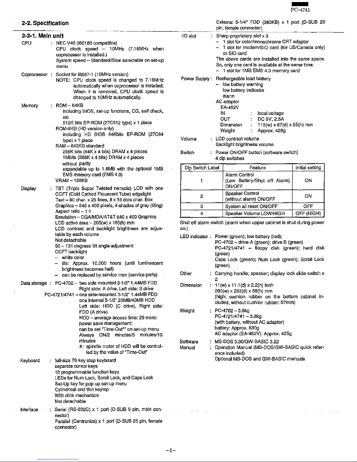
2-2. Specification
2-2-1. Main unit
.~
__________
pin,
female
connecter)
CPU
NEC V40 (i80188 compatible)
CPU
clock speed - 10MHz
(7_16MHz
when
coprocessor
is
installed.)
System
speed -Standard/Slow
selectable
on
set-up
menu
Coprocessor Socket for i8087-1
(1
OM
Hz version)
NOTE: CPU clock speed
is
changed
to
7.16MHz
automatically
when
coprocessor
is
installed.
When
it
is
removed,
CPU
clock
speed
is
changed
to 1 OMHz
automatically.
Memory
ROM
- 64KB
including
BIOS,
set-up
functions,
eG,
self
check,
etc
512K bits EP-ROM (27C512 type) x 1 piece
ROM-8KB (HD
version only)
including
HD
BIOS 64Kbits EP-ROM (27C64
type) x 1 piece
RAM
- 640KB standard
256K bits (64K x 4 bits)
DRAM
x 4 pieces
1 Mbits (256K x 4 bits)
DRAM
x 4 pieces
without
parity
expandable up to 1.6MB with the optional 1
MB
EMS
memory card (EMS
4.0)
VRAM-128KB
Display TST (Triple Super Twisted nematic)
LCD
with one
CCFT (Cold Cathod Flouecent Tube) edgelight
Text -80
char. x 25
lines,
8 x
16
dots
char.
Box
Graphics - 640 x 400 pixels, 4-shades of gray (tiling)
Aspect
ratio
-1:1
Emulation - CGAlMDAlAT&T 640 x 400 Graphics
LCD active area - 205(w) x 155(h)
mm
LCD contrast and backlight brightness are adjustable by each volume
Not detachable
90
-131
degrees tilt angle adjustment
CCFT backlight
-
white
color
- life: Approx. 10,000 hours (until luminescent
brightness becomes
halD
can
be
replaced
by
service
man
(service
parts)
Data
storage
: PC-4702-
two
side-mounted
3-1/2"
1.44MB
FDD
Right
side: A drive,
Left
side: B drive
Keyboard
-Interface
PC-4721/4741 - one side-mounted 3-1/2"
1_44MB
FDD
one internal 3-1/2" 20MB/40MB
HOD
Left side:
HOD
(C
drive),
Right side:
FDD (A
drive)
HDD
-
average
access
time:
29
msec
power
save
management:
can
be
set
"Time-Out*"
on
set-up
menu
Always
ON/2
minutes/5
minutes/10
minutes
:1::
spindle motor of
HOD
will be control-
led by the value of "Time-Out"
full-size 79-key step keyboard
separate
cursor
keys
10
programmable
function
keys
LEDs for Num Lock, Scroll Lock, and Caps Lock
Set-Up
key
for
pop-up
set-up
menu
Cylindrical and thin keytop
With
click
mechanizm
Not detachable
Serial (RS-232C) x 1 port (D-SUB 9 pin,
maleJX>D,
nector)
Parallel (Centronics) x 1 port (D-SUB 25 pin, female
connector)
-5-
lIO
slot
Sharp
proprietary
slot
x 3
- 1
slot
for
color/monochrome
CRT
adaptor
- 1 slot for modem/SIO card (for US/Canada only)
or
SID
card
The
above
cards
are
installed
into
the
same
space.
So,
only
one
card
is
available
at
the
same
time.
- 1
slot
for 1 MB
EMS
4.0
memory
card
Power Supply: Rechargeable lead battery
-
low
battery
warning
low
battery
indicator
alarm
AC adaptor
EA-452V
IN
local voltage
OUT
DC
9V, 2.5A
Dimension 115(w) x 67(d) x 55(h)
mm
Weight Approx. 425g
Volume
LCD
contrast
volume
Backlight
brightness
volume
Switch
Power
ON/OFF
button'
(software
switch)
4
dip
switches
Dip Switch Label
Feature
Initial
setting
Alarm
Control
1
(Low BatterylShut off Alarm) ON
ON/OFF
2
Speaker
Control
ON
(without alarm) ON/OFF
3
System all reset ON/OFF OFF
4 Speaker Volume LOW/HIGH
OFF (HIGH)
Shut
off
alarm
switch
(alarm
when
upper
cabinet
is
shut
during
power
on.)
LED
indicator
:
Other
Dimension
Weight
Software
Manual
Power (green); low battery (red);
PC-4702 -
drive
A (green); drive B (green)
PC-4721
14741
- floppy disk (green); hard disk
(green)
Caps Lock (green); Num Lock (green); Scroll Lock
(green)
Carrying handle; speaker; display lock slide-switch x
2
11
(w) x 11.1
(d) x
2_2(h)
inch
280(w) x 282(d) x 58(h) mm
(high:
cushion
rubber
on
the
bottom
cabinet
in-
cluded,
without
cushion
rubber:
57mm)
PC-4702 - 3.6kg
PC-47?1/4741
-3_8kg
(with battery, without AC adaptor)
battery: Approx. 830g
AC adaptor (EA-452V): Approx. 425g
MS-DOS 3_30/GW-BASIC
3_22
Operation Manual (MS-DOS/GW-BASIC quick refer-
ence
included)
Optional MS-DOS and GW-BASIC manuals
-
--------=~~~~4M~~-----------------------------------------------------------------
Internal
Options:
~.
CE·471
A
color/monochrameCRTad~ptor.
-
color/l1)~mC?_chrC!ITIe
2
m~~~~-.$,uppo~ed:
"
colo(:CGA(640,~209pi~els).
;,
monochrome:
MDA
(720
x
350'pix~ls)
, .
C?P'9~!~or'}02h,rom.~
l!Iode
j~
~f1!~¢e~
by:
~e~-up
functions.
-
2:,sh~racter
sets
(CG1!9<;3,,)
supported
CG1:gen
era
k:,
,
."
CG2:
Denmark/Norway
.'
,.
, .
CG1/CG2
is
selected
bYShort'pin
switch
on
ihecarci: '
dealer
option
...
:_'---"...-
..
.:..
--
-'
J:
',.
~
CE·451 B SIO
card
-
Serial
(RS·232C)
x 1 port
(D·SUB
?§piQ"
1)1~'e
connector)
-
dealer
option
'-i>
'.
NOTE:
Max.
SI02
po~rts.ay.ailable
when
CE:451 B installed.
1.
Stanc!ar~SIQ(/)·SUB
9pin,
mal~,qonnector)
,2.,.SIO,p.nJhe,pptionai
CE'~5~B
SIO
card
(D·SUB
25pin,
mal~,.c\:mne.ctorL
CE-471 B EMS
memory
card
, ,
-
1MB
EMS
4.0
memQryeard
and.EMS4.P,soitware
-
with
OP€!f~~onmcln~_al,
_"
-
dealer
option'
.
CE·462M
modem
card (for
US/Canada
only)
~
ri'lIjci~/S_IO
2.
functions
~lip'Rorted
mode:
300/1200/2400
BPS;
Bell
103l212A;
CCITT
V.21 , V22
and
V.22,
bis
Hayes
compatible
command
set
SlO:-RS·232C x 1 port
(D·SI,I~25
pin,
male
connector)
modem/SIO
function
is
se1ectE!9,QY
set~up
functions
-
;dealer
option
-
'with
installation
instrudions
NOJE:.M'IlUl{C;l',2
porj~avaliabJ$:When
CE·462M
i$
installed
,and,us~d:
asa
510,
' " . ,
1.
Standard
SIO
(D·SUB 9 pin,
male
connector)
2,
SIO
on
the
optional
CE·462M
modem
card
(D·SUB
25
pin,
male
·c?nnectorj· ,
Extem,aJ,ppti,?ns:
;
,I.
,
CE·452F
5·1W
FDD
unil
(without
SEEG)
- 5,114"
~DD
(360KB)
x 1
- ACpower
-
with
I/F
cable
Manual:
CE·470KElFIWIMIS
key.fdp
kit -
-
key
top
(E:
18,
F:
21;
W:
19,
M:
19,
S:
24
pieces)
-iodlforpullirig
up
the
key
t6p
CE-470SElF/Gil·dp~ration·n\8J1Jal
-
operation
manual
for
PC4700
series
(E:
English,
F:
French,
G:
G~rman;
I:
italian)
NOTE:
PC·4700
for SEES doesr't
indludeiheop~ration
manual.
.
\;.'
"!):'ij
; )
oj,
)
,
J"
,,;- ,
'"
1)1"
'~',
'
-6-
.....
I
'2
r·····
-:
HID
: ROM
.2
'------
RS22C
I/F
I
9pin
I
SLOT
(AI
I I
ocv,
\0,
~
20,~~z
14.3,);',MHz
I CE-471A I I CE-451B 1,.8432
~
rD'J
riDh
I . .
CE-462M
I
MHz
ADO-7F I
II
• -
~-
---'
INSS2C50A
X1~~::::::~~~~~~~~~~.§!~~~50;P,"~I~I~
~~~1'34~p;~n~i
~~D~~~UA;R~Tl;;~~;j
AS-19 A ILIl=f I
1m
D
---'
(JPD7020B-10
_______________
: ('21
~
~
~
~------
~
=
:~
Opt;onal
i-.-
I-
I
'------'
HD
Co-Pm,e.,o,:
LZ95H12
-----,
8071-1
~
(Gale
array)
---
...........
:
Video
BIOS
ROM
I--
DRAM
- LZ93J21 FDC
(64KB)
1=
(12BKS)
(Gale array)
,......
_____
. 27C512
I+-
16MHz
~
.S
.
256Kbn
X 4
~
TCS566F
~.
I
____
, l
System
I--
f--
L~M~U:XJ------I
DRAM
F=
(640KBI
[+-j
Hf--I--~
~
1MbilX4
r-
256Kbit
X 4
,
______
. I
Dd,e'
i
f=='
I
('11
"d
disk
with
interface
i SLOT
(CI
i-----J 3.S4MHz
~
-System/Key bo",d
~
3.5 ;n,h
! CE-471B
~
-RTC
~
floppy disk drive
I 32.76SKHz g I
1.44MB
. 34p;n L Conlmlle,
'7
L D .
.---'---
1.
______
,..;
LU57S44P
/
AMP
,,,e,
l Driver 1
,
----r~Wh1
VCC
L 25p;n
'\
r--:
~
_
VGG
r:::L-----c
r:::::::,
Pr;nte,IIF
Power
supply
VCRT
r--~
LCD
unit
f--
Keyboard
SPEAKER
640
X 400
GND
_
'-
______
----1.,2V
(~1)
PC-4702: 2
drives
PC-4721/4741 : 1
drives
(·2) PC-4721/4741 only
mlo
rl::E:
OIl>
o "tI
'"
-I
t:I
m
;;: :xl
G>
(,0)
JJ
I •
>3:
21:l>
1-
Z
III
o
l>
:xl
C
o
"tI
m
:xl
~
o
z
21
;;;:!
>"

-
3-1. Memory and I/O map
3-1-1. Memory
map
for
the PC-4700 system
FFFFFh
r------,
ROM-BIOS
FOOOOh
\-----\
E7FFFh
EOOOOh
DOOOOh
C9FFFh
CeaaOh
BFFFFh
BBFFfh
88000h
BOFFFh
BOOOOh
9FFFFh
ooaDah
EMS
window
HD
ROM
BIOS
System
Rsvd
eGA
Video
Memory
System
Asvd
~QA
Video
Memory
Standard
Main
Memory
: 640KB
20000h
Fig.
3-1
Overall memory
map
3-1-2.10/MAP
Register,
Emulate~
DMA
Controller
V40DMA Controller
Interrupt Controller
System Timer
PPI
NMI
Mask
Asynchronous Communication (Secondary)
Hard Disk
Parallel Port
Parallel Port
VIDEO
10
VIDEO
10
VIDEO
10
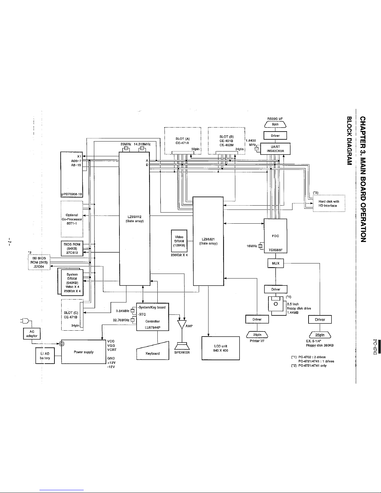
VIDEO
10
FLOPPY DISK
10
Asynchronous Communication
(Primary)
V40
System
10
3-2.
Clock
generator
:
maximum
768KB
EMS
Memory
(1MB)
10
Address.
OOHnOFH
10HnlFH
20Hn3FH
40H
..
5FH
60H
..
62H
AOHnBFH
2FBHn2FFH
320Hn323H
37BH
..
37FH
3BCH
..
3BEH
3BOH
..
3BBH
3BFH
3COH
..
3CFH
3DOH
..
3DFH
3FOH
..
3F7H
3FBH
..
3FFH
FFFOH
..
FFFFH
The
cloc)~
generator
is
includetfin~bZ95H-1·2.-·and-~nnecte'd
with-tWo"~--~
crystal oscillators of
14.3181
BMHz
and
20MHz.
The
two
clocks pass through
the
clock select drcuil
in
LZ95H12,
and
one of them is outputted from
Xl
terminal to
V40·
Xl
termi,liar.
,The
details are
shoWn
in
Fig.
3-2.
~Ji-
20MHz
CEoseD._
-
"-
~ ~ ~
-
=
CPOSC1
Clock
- X1·
.
X1
14.3181BMHz
select
NC'X2'
V",
OSCD
circuit
=
aSC1
Bus
cycle
CPUCLK
CLKOUT
LZ95H12
generator
SYSCLK
Fig.
3-2 Overall clock generate circuit
The frequency
\If
,he
clo¢k
~ypplied
from
LZ95H12
Xl
terminal
to
V40
is
determined according
to
the
states of bit 3
(OSCSPD1)
and
bit 2
(OSCSPDO)
of the
10
port
(7BH)
in
LZ95H12
as
shown
below.
7654320
X X X X \x\x 107BH(RIW)
a
20MHz
Assertion of
the
RESET signal will reset
OSCSPD
[0
..
1]. IF
BOB7
is
not installed, ROM·BIOS sets
OSCSPOO.
When
setting
OSCSPDO,
the shift to frequency of
10MHz
is
made
wtth
no
!;Ittches, thus avoiding
the
need
to
reset the
system.
3-3.
~eset
circuit
SCM
(LU57844)
R
ET
LZ95H12
l.Z93J21
RES
TCS566F
OUT
'
B2C5OA
V
CN7-28{34-pin
slot)
CN8-49{CRT
connector)
eNS·1
(HOD
connector)
Fig.
3-3 Reset control circuit
The
SCM
can
be
reset
in
one of the following two
ways.
1.
When
VGG
turns on, a high state
of
signal is sent
to
the
line
ACL
of
the
SCM
from the differentiation circuitry
composed
of a
capacitor
and
resistor.
2.
When
the
dip switch-1.located at the lower
side
of
the
machine,
set
ON,
it causes the
ACL
input
high
to
reset
the
SCM.
Operation
starts
when
it turned off.
With
depression of the ON/OFF switch while
1he
machine
is off or a
hardware reset is given (simultaneous
depres'sion
of
CTRL,
AL
T,
SETUP
keys),
VCC is turned active
and
RESET is
forced
high.
The
V40
synchronizes
an
async signal RESET
with
the internal clock
and
sends it out
as
an
active high signal.
The fdrmer (RESET) is sent
to
the
V40,
and
the
latter
(RESET)
to
the
LZ95H12,
LZ93J21,
TCB566F,
B2C50AV,
34'pin slot,
CRT
connector.
The
RESET
signal is inverted
and
sent
to
HDD
connector.
3-4. Interrupt control
Eight maskable interrupts
and
one non-maskable interrupt
are
provided. .
NMI
is
set high by the LZ95"'12 when a
sp~cific
VO
is accessed.
• Maskable interrupt
may
be
caused
in
one
of
the
following:
Numbe:r
Usage
Originating device
1
KeyboarQ
LZ95H12
3
Asynchronous communication
(Secondary)
INSB2C50A
4
Asynchronous communication
(Primary)
5 Hard disk
Hard
disk controller
6 Floppy disk
TCB566F
7 Parallel printer
LZ93J21
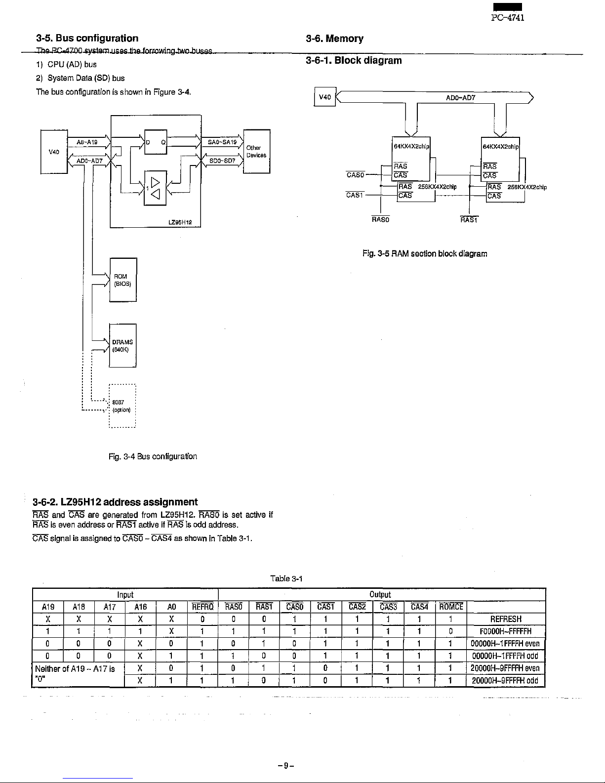
3-5.
Bus
configuration 3-6. Memory
-
PC-4741
~~~D~~.~orDlWmgJwnbul's.~s~
________________
~~~~~~~
____________________________________
__
1)
CPU
(AD)
bus
3-6-1. Block diagram
2)
System
Data
(SO)
bus
The
bus
configuration
is
shown
in
Figure
3-4.
V40
ADO-A;e0c-'
-.II\~
ROM
(BIOS)
DRAMS
(640K)
--"-':; 808:
"'--"1':
(optIOn)
1-_-;l'I-'S",AO:.-=SA.:.:':,'
II
Other
,--,\It'-;==:;"\J
Devices
500-507
LZ95H12
Fig.
3-4
Bus
configuration
3-6-2.
LZ95H12
address assignment
RAS
and
CAS
are
generated
from
LZ95H12.
RASO
is
set
active
if
RAS
is
even
address
or
RAS1
active
if
RAS
is
odd
address.
CPS
signal
is
assigned
to
C'ASl5
-
CAS4
as
shown
in
Table
3-1.
Table
3-1
Input
A19
A1B
A1l
A1B
AO
mAll
RASO
RAS1
CASO
X
X
X X
X
0
0 0
1
,
1 1
1
X
1 1
1
1
0
0 0
X 0 1 0 1 0
0 0
0
X 1
,
1
0
0
Neither
of
A19
-A17
is
X
0
,
0
1
,
"0"
X 1 1 1 0 1
-9-
v401'--
________
,
ADO-AD7
64KX4X2chlp
64KX4X2chip
Fig.
3·5
RAM
section
block
diagram
Output
GAS'
GAS2
CAS3
i;AS4
ROMCt
1 1
1 1
1
REFRESH
,
1
1 1 0
FOOOOH-FFFFFH
,
1 1
,
1
OOOOOH-1
FFFFH
even
, ,
1
, ,
OOOOOH-1
FFFFH
odd
0
,
1 1
1
20000H-9FFFFH
even
0
1
1 1 1
20000H-9FFFFH
odd

-
--------~~:'!74~t~'
--------------------------------------------~--------------------~------
3·6·3
Memory
access
timing
<D
Normal DRAM access
T2
CLKOUT
. 1
'.,
30-40
30-40
MA;
ROW
Address
,:.Co!umn
Address
r~-
-',-,
'
'-,
C \
--30--40:'
flg::H
DRArvr~q"esj!timi[lg
(normal)
@ At DMA memory write
CLKOUT
- 0''-'
BS
10-55
10-55
10-20
30-50
Same as
<D
for the timing
of
OE, WE, RAS, and MA.
Fig. 3-7 DRAM access timing (DMA memory write)
® ROM access
CLKQUT
A1B-A19
_I-Ij\...::::!:::.::~'+
_____
+-----
10-20
20-40
20-40
Fig.
3-8
ROM
access
timing
3·7_
8087
interface
The
interface
log
of
8087
is
stored
in
LZ95H12.
The
signal
connection
is
shown
in
Fig.
3-9.
r;:::==1
aso
-aS1
V4O"
.
'.
8087
ADO-AD7
A8-A19
NMI~"++
~
ADO-AD7
A8-A19
READy'I-----------
__
--.J
Fig.
3~9
8087
interface
signal
connection
3·8.
READY
control
circuit
The signal
READY(RDYll40):Jor
WOis
.contralled bY.LZ95Ht2.
LZ95H12 and LZ95J21 control EXTM, EXTIO, SLOCYC, and
~EADY
signals
for
the
devices
accessed.
LZ95H12
determines
'tne
bus
cycle
according
to
these
signals,
to
control
RDYV4d.
The
bkick
diagram
is
shown in Fig. 3-10. ;
...
c:
.:
:1
•
AOO-AOZ
SOO-S07
:
SAO-SA19
vila
Fig.
~-1
0 Overall ready control signals
3·9.
DMA
control
!293J21
Although the V40
haS
faurDMA channels, two i:hannels are used.
DRQ2 and DACK2 are used for controlling the floppy.
DRQ2
"-
DACK2
V40
DATA
BUS
TCS566F
(~PD70208G)
H
(FDC)
Memol}'
Fig.
3-11
Overall DMA control
~ignals
. ,
When the V40 starts to DMA after setting 'the TC8566F register, the
TC8566F sets DRQ2 high. After the V40 receives this signal, DACK2
is
set
low
to
perform
DMA
transfer
between
the
TC8566F
and
the
memory.
DRQ3 and DACK3 are used for controlling the hard disk. DRQ3
is
supplied from the LSI in the hard disk controller. When DRQ3 be-
comes
high,
V40
makes
DACK3
low
to
perform
DMA
transfer
be-
tween
with
the
controller.
,
3·10.
Bus
cycle generator (including
LZ95H12)
3·10·1.
General
The LZ95H12 bus cycle generator produceslhe SYSCLK,"
ALE,"
STC,
SMRD, SMWR, SIORD and SIOWRsignals:
11
inte.preisflie READY
signal
and
drives
thf;)
RDYV40~s_ignal
to'_controI
th'~
number"c,f
wait
states.
The
LZ95H12
det~rmines
the'speEtd'of
the
devices
involved
in
the
transfer.
Deviees,
are
group-eo
intoJhree
speed
categories:
1.
fast
AD
bus
devices;
2.
fast
SD
bus
devices;
and
3.
slow
SO
bus
devices.
i=ast.AD devices are the V40, the
SOS7,_the
LZ9.5H12,
the system
ROM, the system DRAM. Fast
SO
bus devices are those devices
Wniphare qqQtrbli!fdi;fy the LZ93J21!ar which the
SL0CYC
signal
is
nat asserted. This signai is sampled
altha
start
of
first T-cycle fallow-
ing
,the
assertion·
01
th&SMRD,
SMWR, $IORD or SIOWR. At
7.16MHz, this occurs at the start
of
T:3.
Ai
10 MHz this occurs at the
S!~rt
of
the'first
TW~_'~IJ
othe(ce~ices
~re
slow
SO
bus
devices.
Th~rl?
are
ti1r~e
SPE;!~c:f~,-of
11.~"n-r~fr~sh~cyqiE;!s:
la~t,
medium
~lI:u;f
slow.
Fast
speed
cycle
execute
with
no
wait
states,
.9xcE!pt"for
;IQ,NMI
trapping
cycles;-whicfi"take
'nine
T-cycles.
'Medium
speed
cycles
may
--
aiso"insert
wait
states
in
resp·onse
to
a.'-reset
READY
signal. A special
extended medium speed cycle that drives SYSCLK fram CPUCLK
is
also implemented. At 7.16 MHz, the minimum medium speed cycle
takes 5 T-cycles. At 10 MHz, the minimum medium speed cycle takes
6 T-cycles. Medium and slow speed cycles have the same timing until
SLOCYC
is
sampled.
-10-
If the CPUSPD (107BH bit 1) bit is set, the bus cycle generator will
only
generate
slow
speed
memory
cycles.
This
is
done
to
accorn-
-
mod
ate
programs -uSing
softWare
timing
loops.
Assertion
of
the
RESET signal will reset CPUSPD. If CPOSPD is reset, then speed
of
the
cycle
is
dependent
on
the
slowest
device
involved.
If
the
slowest
device
is a fast
AD
QY§
device
then a fast
speed
cycle
is
generated.
If
the
slowest
device
is a fast
SO
bus
device.
then a medium
speed
cycle
is
generated. Otherwise, a
slow
speed
cycle
is
generated.
When
"speed:
slow"
is
selected
in
the
set
up
menu,
CPOSPD
_ 1
(High)
There are two speeds for refresh cycle-fast and slow. If the EXTREF
(107BH bit
6)
bit
is
set, the bus cycle generator will generate a slow
speed cycle. Thus DRAM on the SD bus may be refreshed. If EXTREF and CPUSPD are reset, then the bus cycle generator wili
generate a fast speed cycle. Thus any DRAM on the SD bus must
provide
its
own
refresh.
Resetting
EXTREF
may
result
in
as
much
as
a
5%
increase
in
system
throughput.
Assertion
of
the
RESET
signal
will reset EXTREF. When the optional EMS card (CE-453B) is in-
stalied, EXTREF
= 1 (High).
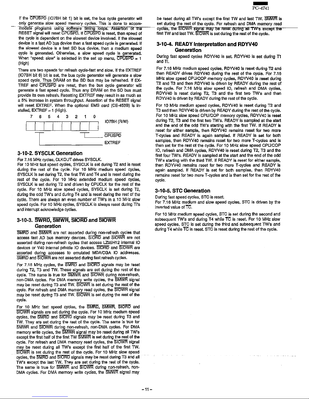
7654320
I I
T
T
3-10-2.
SYSCLK
Generation
For 7.16 MHz cycles, CLKOUT drives SYSCLK.
107BH
(R/W)
CPUSPD
EXTREF
For 10 MHz fast speed cycles, SYSCLK is set during T2 and is reset
during the rest of the cycle. For 10 MHz medium speed cycles,
SYSCLK is set during T2, the first TW and T 4 and is reset during the
rest
of
the
cycle.
For
10
MHz
extended
medium
speed
cycles,
SYSCLK
is
set during T2 and driven by CPUCLK for the rest of the
cycle. For
10
MHz slow speed cycles, SYSCLK
is
set during T2,
during the odd TW's and during T4 and is reset during the rest of the
cycle.
There
are
always
an
even
number
of
TW's
in a 10
MHz
slow
speed cycle. For 10 MHz cycles, SYSCLK
is
always reset during TI's
and
interrupt
acknowledge
cycles.
3-10-3.
SWRD,
SMWR,
SIORD
and
SIOWR
Generation
'S'MR15
and
~
are
not
asserted
during
non-refresh
cycles
that
access
fast
AD
bus
memory
devices.
SIORD
and
SIOWR
are
not
asserted
during
non-refresh
cycles
that
access
LZ95H12
internal
10
devices
or
V40
internal
private
10
devices.
'STOFfi)
and
SIOWR
are
asserted dUring accesses
to
emulated
MDNCGA
10
addresses.
SMRD and SIOWR are not asserted during fast refresh cycles.
For 7.16 MHz cycles, the
SMRD
and S1OR5 signals may be reset
during
T2,
T3
and
TW.
These
signals
are
set
during
the
rest
of
the
cycle.
The
same
is
true
for
SMWR
and
SIOWR
during
non-refresh,
non-DMA
cycles.
For
DMA
memory
write
cycles,
the
SMWR
signal
may
be
reset
during
T3
and
TW.
'Si'OWR'
is
set
during
the
rest
of
the
cycle.
For
refresh
and
DMA
memory
read
cycles,
the
~
signal
may
be
reset
during
T3
and
TW.
SIOWR
is
set
during
the
rest
of
the
cycle.
For 10 MHz fast speed cycles, the
ll1iiIFID,
~,
SR5lm
and
SIOWR signals are set during the cycle. For 10 MHz medium speed
cycles, the
ll1iiIFID
and
S1OR5 signals may be reset during T3 and
TW.
They
are
set
during
the
rest
of
the
cycle.
The
same
is
true
for
~
and
"SlOWR
during non-refresh, non-DMA cycles. For DMA
memory write cycles, the SMWR signal may be reset during ali TW's
except the first half of the first
TW
$Ii;1WI'i
Is
set during the rest of the
cycle. For refresh and DMA memory read cycles, the
"SlOWR
signal
may be reset during ali TW's except the first half
of
the first TW.
SIOWR is set during the rest
of
the cycle. For 10 MHz slow speed
cycles, the
ll1iiIFID
and
SR5lm
signals may be reset during T3 and ali
TW's except the last TW. They are set during the rest
of
the cycle.
The
same
is
true
for
S'KifWF1
and
'S1OWR'
during
non-refresh,
non-
DMA cycles. For DMA memory write cycles, the
~
signal may
-11-
-
PC-4741
be reset during all TW's except the first
TW
and last
TW.
SMWI'!
is
set
during
the
rest
of
the
cycle.
For
refresh
and
DMA
memory
read
cycles;t11e
SIOWRSIgfiliImayOe
reset
darlng-1!ll1"W'ln!"i<Cl!l1ptrttl1l
,01.---
first
TW
and
last
TW.
Sf'OWR
is
set
during
the
rest
of
the
cycle.
3-10-4.
READY
Interpretation
and
RDYV40
Generation
During fast speed cycles RDYV40
Is
set. RDYV40 Is set during
T1
andT!.
For 7.16 MHz medium speed cycles, RDYV40 Is reset during T2 and
then READY drives RDYV40 during the rest
of
the cycle. For 7.16
MHz slow <peed CPU/COP memory cycles, RDYV40
is
reset during
T2 and T3 and then RDYV40 Is driven by READY during the rest
of
the cycle. For 7.16 MHz slow speed
10,
refresh and DMA cycles,
RDYV40 Is reset during
T2,
T3 and the first two
TW's
and then
RDYV40
is
driven by READY during the rest
of
the cycle.
For
10
MHz
medium
speed
cycles,
RDYV40
is
reset
during
T2
and
T3 and then RDYV40
is
driven by READY during the rest
of
the cycle.
For 10 MHz slow speed CPU/COP memory cycles, RDYV40 Is reset
during T2, T3 and the first two TW's. READY is sampled
at
the start
and the end
of
the odd TW's starting with the first TW.
If
READY
Is
reset for either sample, then RDYV40 remains reset
for
two
mar.
T-cycles and READY is again sampled. If READY
is
set
for both
samples,
then
RDYV40
remains
reset
for
two
more T --cycles
and
is
then set for the rest
of
the cycle. For 10
MHz
slow speed CPU/COP
10, refresh and DMA cycles, RDYV40 is reset during T2. T3 and the
first four TW's. READY
is
sampled at the start and the
end
of
the odd
TW's
starting
with
the
third
TW.
If
READY
is
reset
for
either
sample,
then
RDYV40
remains
reset
for
two
more
T-cycles
and
READY
is
again sampled. If READY is set for both samples, then RDYV40
remains
reset
for
two
more T -cycles
and
is
then
set
for
the
rest
of
the
cycle.
3-10-5_
STC
Generation
During
fast
speed
cycles,
STe
is
reset.
For
7.16
MHz
medium
and
slow
speed
cycles,
STe
is
driven
by
the
inverted
value
of
Te.
For 10 MHz medium speed cycles, STC
is
set during the second and
subsequent TW's and during T4 while
m is reset. For
10
MHz slow
speed cycles, STC is set during the third and subsequent
TWs
and
during
T 4
while
Te
is
reset.
STe
Is
reset
during
the
rest
of
the
cycle.
3-'0-6;
Timing chart
$7.1.6:MHzMEElIUM
cyCle
~I
,
SVlD,~
SMWR
SIOWR-DMACYCI:.ES
.
,~'-,
,
Ti'
"JI
I
",
T~
1
I
-
>',
,J
t:i
TW
T4
I
I.'
•
I
, :
-(
I~::
I;
'
••
!---'-!
--II
'.
i
STC
---------------------;-,,-'---,-'---li:.:
···~~;i~~;~~,:··.-·:·l::
SVLD
IS
HIGH
AT
•
FALLIMG
EDGES
:
,OFCPUCU(
,I
RDYV40, -•• -•• -•• -•• -••
-:.P::;.R::;,!V"'"E""N"",,"~"''f.7.1,Z'''
..
9:::,5::-,H:':',1,2::-
..
-:.-".;.
•. -..
,...,,,t,'''
.....
''''
....
,,,
...
I
...
,.,''~
..
!
....
''''"
....
!?fllY.~!'!,~Y..I)~[';[)'f....
.............. ,
......
.
@7.16
MHz
SLOW
cycle
(CPU-MEMORY
cycle)
T1
CPUClK
LJ
SVlD
SYSClK
LJ
ALE
SMWR
SIOWR-DMA
CYCLES
T2
, ,
, ,
READY=l
SlOClY=O
T3
TW
T4
LJ
1
r·~~;~~~~~lb~,···-.·-1-
:
REPEATED
WHILE
:
!
SVlDIS~IIGHAT
':
•
FALLlMG
EDGES'
;,
:
OFCPu(:LK" -..
:
RDYV40
"",
........
!?~!y'~.N,
~'f.
,1,Z,~?~.1.?",
,I
..................
',.
i
.... " ......
,,,,_,,,,
1 en,' :
•.
) .•
en!?~!y.~!'!.~Y
..
I),~[';[)y
•••
'en
:"'.m.en,
..
u
READY=1
SlDClY=O
-12-
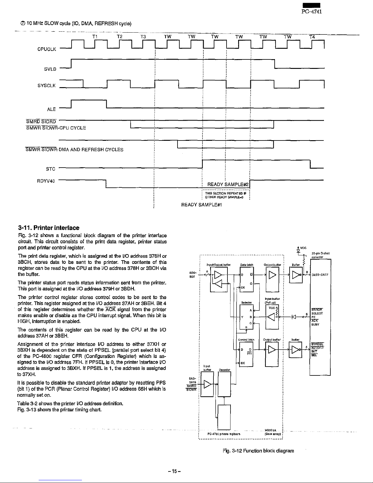
® 7.16
MHz
SLOW cycle
(10,
DMA,
REFRESH cycle)
CPUCLK
SVLD
~
SYSCLK
ALE
-
PC-4741
SMRDSIORD
----------------,-------~----------------------------~--~------+--------
SMWR
SIOWR·CPU
CYCLES
SMWR
SIOWR·DMA
AND
REFRESH
CYCLES
iTHisf;EcnON--·
j
~~~~~~~~G~H!~:
L
STC
______________________
~---J
:
FALLlMG
EDGES
:
OF
CPUClK
RDYV40
.................................
l
............... , .............
O'R.I.~~~.B.Y.~9.~~1~
.........
1
......
T
.........
~.I:'I!!!!'t>I.~:-!.f!IO!I.D:-!
......
.
READY=1
SLOCYC=1
® 10 MHz MEDIUM cycle
T1
T2 T3
TW
TW
T4
CPUCLK
n n n n
n
I
I
SVLD
----'
SYSCLK
________
~
______
-J
ALE
-----'
SMRDSIORD-------------------------------.----------~--~----~---------+--------
SMWR
SIOWR·CPU
CYCLES
SMWR
SIOWR·DMA
CYCLES
'·"THis·sECTioN"'--
i
STC
-----------------------------------------;----+---~i
~e~~~~G~H1~E
l
, • :
FALlIMG
EOGES
:
L
, : .
ww®w
.
. .
Ro.y'l~O
·····
...
···
.............
·····•··
..
··
..
·····f········gB!Y~ft~XH~].~.1L
•.•
I.··.·R:~t~~:[lR.I.\I!'t>I.~:-!.f!!'''I?:-!
.•.•..•...••. : ... : ...
::
.
SLOCYC=O
-13-
@
10
MHz
EX1ended
MEDIUM
cycle
'"
T-,"1-..",="').
T-=-2
."....;.'" T3
.•
':
r
U-
,,--I
-<--J:-~n
;T:W
·----1
r
TW
T4
r:==J""""..,.,-J1l
-
..
"-_.
----,--
.
.-
~
$VUL-.----'
SYSC1K
1
:
..-1
-+--,n!--,-.
--Ii
ALE
, ,
,
,
-~
~~~-<'"~--~---~
.-~
-
.J
, ,
, ,
,
,
, ,
SMRD SIORD
SMWR
SIOWR-CPU CYCLES
-
'---L-I
----7"------:---+--'--,.--
..
--.
~
r"
)
I]
J
, ,
RDYV40
.''''
'Uo.",,' ",uuuun' '''''.UUn''' I
......
u:~.R:il[!;N
.~:!.l.,i~~fj1
g~
..
U ! . U
.. ' u.
i
.........
u ....
uD.I'IIIJ!;N
.~.Y.
flE,.I\.[)L.
u.····u
@ 10
MHz
SLOW
cycle
(CPU-MEMORY
cycl~)
CPUCLK
SVLD
SYSCLK
__
L-----',
ALE
SMRD
SMWR-CPU CYCLES
RDYV40
1
READY=1
SLQCYC=O
REDY SAMPLE
#2
-i·'THls·s-ecrlo;'-REPEATEi)iF··
:
EITHER
READY
SAMPlE=O
SLOCYC=1
READY SAMPLE
#1
-14-
I
<1J
10
MHz
SLOW
cycle
(10,
DMA,
REFRESH
cycle)
CPUCLK
SVLD
SYSCLK
ALE
-
PC--4741
SMRDSIORD
--------------------~----~------------~-----+------+-----_r--------------
SMWR
SIOWR-CPU
CYCLE
SMWR
SIOWR-DMA
AND
REFRESH
CYCLES
STC
RDYV40
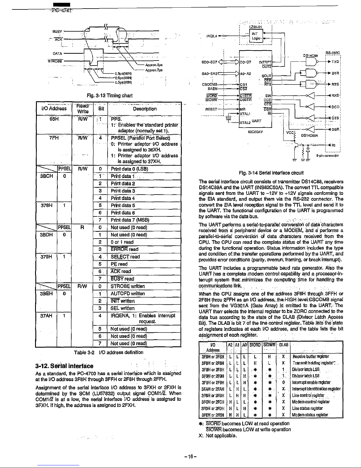
3-11. Printer interface
Fig,
3-12
shows a func1ional
block diagram of the printer interface
circuit. This circuit consists of the print data register, printer status
port
and
printer
control
register.
The
print data register, which
is
assigned
at
the
110
address
378H
or
3BCH,
stores data
to
be
sent
to
the printer.
The
contents of this
register
can
be
read
by the
CPU
at the
va
address
37BH
or 3BCH via
the buffer.
The
printer
status
port
reads
status information sent
from
the printer.
This
port
is
assigned at the
110
address
379H
or
3BDH.
The
printer control register stores control
codes
to
be
sent
to
the
printer. This register assigned at the
110
address 37AH or 3BEH. Bit 4
of this register determines whether the ACK signal from the printer
makes
enable or disable
as
the
CPU
interrupt signal. When this bit is
HIGH,
interruption
is
enabled.
The
contents of this register can
be
read
by
the
CPU
at the
110
address
37AH
or
3BEH.
Assignment of the printer interface
110
address
to
either 37XH or
3BXH
is dependent
on
the state of PPSEL (parallel port select bit
4)
of the
PC-4600
register
CFR
(Conffguration
Register)
which
is
as-
signed
to
the
1/0
address 7FH.
If
PPSEL
is
0,
the
printer interface
110
address
is
assigned
to
3BXH. If PPSEL
Is
1.
the address
Is
assigned
to
37XH.
It
is
possible
to
disable the standard printer adaptor by resetting
PPS
(bit 1) of the
PCR
(Planar Control Register)
110
address
65H
which is
normally set
on.
Table 3-2 shows the printer
110
address definition.
Fig.
3-13 shows the printer timing chart.
-15-
READY
SAMPLE#2
THIS
SECTION
REPEATED
IF
EITHER
READY
SAM
PLE
.. O
L
READY
SAMPLE#1
SDO~
'"
SAO~
SA15
""'"
"""'"
Inp~VOulpU!
buHer Dala latch Bufler
a
Selec!or
YOO
25-pln
D-she!1
conector
DATO~DAT7
A
."",.,..
y ,
I<----1K
flI<c..;...--1<J--~';'"-I
;~LECT
-
C BUSY
Confrulla1ch
OU1pU!
buffar
B~ffer
InpUL
buHer Deceder
_VG301A
PC
..
HOO
privale
reglSLers
(GaLe
anay)
Fig.
3-12 Function block diagram
BUSY·_~='1_4··~..
i
...........
__
_
.~--ACK
~
.
-~--
;
..
,."
.
DATA
--_~\-L--=3;S~
___
-
STROBE
---+-,)
Appro)(.511S
Approx.7ll
s
Fig.
3-13
TIming
chart
___
~~
__
,_,T'
_"~
-ReaClr-
~--
-"
~-"
110
Address
Write
Bit
Description
sSi-!
"PJW
i 1
PPS:
_0
- .
1,.. Enables-tho"standard-printer
adaptor (normally set
1).
7FH
-FfNl
o
4
0-
- PPSEL
O
(Paraller1'6ri
Select)
...
-O;Printeradaptor-I/O
address
is
assigned
to
36XH.
..
-
1; Printer adaptor 1/0
address
is
assigned
to
37XH.
-----
PPSEL
RNI
0
Print data 0
(LSB)
3BCH
0
1 Print data 1 .
2 Print data 2
3 Print
daia3
4 Print data 4
378H 1 5 Print data 5
6
Print data 6
7
Print data 7
(MSB)
-----
PPSEL
R 0 Not
used
(0
read)
3BDH
0
1
Not
used
(0
read)
2 o
or
1
read
3
Ei'iFiOR
read
379H
1
4
Sl;bECT
read
5
PE.read
6
AeRread
7
.liUSYread
~
PPSEL
RIW
0
STROBE
written
3BEH
0
1
AUTOFD
written
2
mwritlen
3
SEL
wriften
37AH
1 4
IRdENA, 1;
Enables
interrupt
request.
5 Not
used
(0
read)
6 ° Not
used
(0
read)
7 Not
used
(0
read)
Table 3·2
1/0
address
definition
3-12.
Serial
interface
As
a standard, the PC-4700
has
a serial interface
wt1ich
is
assigned
at the
110
address 3F8H
through
3FFH
or
2F8H
through 2FFH.
Assignment of the serial interface
1/0
address
to
3FXH
or
2FXH
is
determined by the
scM
(LU57832)
output signal COMl/2.
When
COMlt2
is
at a
low,
the
serial
interface
1/0
addres,:
is
assigned
to
3FXH. If high, the address
is
assigned
to
2FXH.
-16-
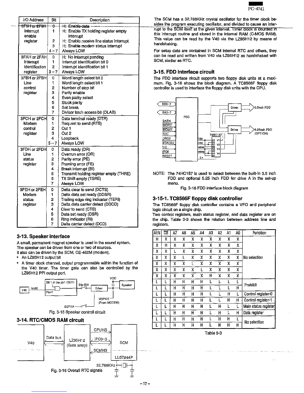
IRQSA
-~--7--'4
SDo--SD7
SAO-SA2
CSCOMB.=~
SAEN
SJOAD
SIOy.'R
i "
RESET
--
...
-----
....
=
---_!_-
••
_------
••••
DS14CB8
f!~:?~?~.
DO~D7
INTRPT
TXO:
aUT2
AO-A2
SOUT
OTR':
DTR
CS1
R'FS
RIS:
CS2
01STR
SIN
!;lOBTA
DCD
CTS
'~~~==~l-::
f--.;-oRXD:
'&-
oeD:
MR
DSR
XTAL1
RI
XTA12 UART
82C50AV
L.."-'-/
jC~+:
:c,j'
-·'GTS
i
_~~~<:~~-.DSR:
DS14C89A
.:1-",",t""'--+-"
RI
'-----.... '
9-pin
connector
Fig.
3-14 Serial interface circuit
The
serial
interface circuit consists of transmitter 0814C88, receivers
DS14C89A
and
the UART
(INS82C50A).
The
convert
TTL
compatible
signals sent from the UART to
-12V
to
+ 12V signals conforming to
the
EIA
standard,
and
output
them
via
the
RS·232
connector.
The
convert
the
ErA
level reception
Signal
to
the
TTL
level
and
send
it
to
the
UART.
The
functional configuration
of
the
UART
is
programmed
by
software via the data bus.
The
UART
p~rforms.
a
serial-to~parallel
conversion
of
dat~d:haracters
receI~ed
fr0
rTl
'
a;
peripherar
device
or
a,
MotiEM.
and
~
,performs
a
pa'ralfel-t6-seriaI
conversidn
of
data
characters
reCeived
from
the
CPU.
The
CPU
can
read
the
complete
St~tus
of the
UART
any time
during the functional
operation~'
Status, information includes the type
and condition oUhe, transfer. operations performed
by,th.8
UART,'
and
provides error conditions
(pari't)',
overrun;
framing,
or
break
interrupt).
The
UART
includes a programmable
baud
rate
generator.
Also
the
UARl'
ras
a complete
.modem
control·.capability
and
a processqr-in-
terrupt
system
that: minimizes.
the·
computing· time
for
handling the
co,rpmu~ic~tions
lin~.
When
.the
CPU
assigns
one
of
the:
address
3FSH
thrQugh
.3FFH
or
2F8H
throu
2FFH
as
an
1/0.address,the,oHIGH
leve~CSC0MB
signal
senUram
the.·VG301
A (Gate
Array)
.is.
emitted
to
the.
UART.
The
UART therr selects the internal register
to..
b.
ZORC
.con.nected
to
the
data
bus
according.
to..
the state of
the
DLAB (Oiviso(
Latch
Aqcess
Sit).
The
DLABis bit 7 of
the
line control register
..
Table lists the'state
of registers indicates at
.each
1/0
address,
and the table lists the
bH
assignment of
each
reglstei'.
.
I/O
.
A2
Al
AD
.
mmm
lmlWI!
·O.LAB
Add"rE!~s,
.
, .
:
3F.8H.or2F8H.
L L
L
L
H
X
3F8H
or
2F8H
L
L L
H L
X
3F8H
or
2F8H
L ~ L
.*
*
1 .
3~9H
or2f9H
L L
H
*
!I'.
1.
3F9H
or
2F9H
L L H
*
*
D
3FAH
or2FAH
L H
L.
,
*
*-
X.
3FBH
or2FBH
L H H
*
.*
X
3FCH
or2FGH
H L
L
*
*
X
3FOH
or2FOH
H L H
*
*
X
3FEH
or2FEH
H H
L
* *
X
*;
SJWiiJ
becomes
LOW
at
read
operation
§ClWR
becomes
LOW
at write
operation
X;
Not applicable.
..
Receive
buffer
register
Transmltholding
re"gismt-:",
Divisor
latch
LSB;
Divisor
ia~~h
L~B
Interrupt
en~ble
register
Interruptidentificatioll
reg!ster
Line
control'
register
"
Modem
control
regi~r
Line
status
register
Modem
status
register
110
Address
Bit
Description
-eF9H~H
-9-
~,
Blable-<iata~
Interrupt 1 H: Enable TX holding register empty
enable
interrupt
register
2
H:
Enable
receive
line
status
interrupt
3
H: Enable modem status interrupt
4-7
Always LOW
3FAH or 2FAH
0
H: No interrupt pending
Interrupt 1
Interrupt identification bit
0
identification
2 Interrupt identification bit 1
register
3-7
Always LOW
3FBH or 2FBH 0 Word length select bit
0
Line
1
Word length select bit 1
control
2
Number
of
stop
bit
register
3 Parity enable
4
Even
parity
select
5 Stuck parity
6 Set break
7 Divisor latch access bit (DLAB)
3FCHor2FCH
0 Data terminal ready (DTR)
Modem
1 Request to send (RTS)
control
2 Out 1
register
3
Out2
4 Loopback
5-7
Always LOW
3FDH
or2FDH
0
Data ready (DR)
Line
1 Overrun error (OR)
status
2 Parity error (PE)
register
3 Framing error (FE)
4 Break interrupt (BI)
5
Transmit holding register empty (THRE)
6 TX Shift empty (TSRE)
7
A'rways
LOW
3FEH or 2FEH
0
Delta clear to send (DCTS)
Modem
1 Delta data set ready (DDSR)
status
2
Trailing edge ring indicator (TERI)
register
3
Delta dala carrier detect (DDCD)
4 Clear
10 send (CTS)
5
Data set ready (DSR)
6
Ring indicator (RI)
7 Delta carrier detect (DCD)
3-13. Speaker interface
A
small,
permanent
magnet
speaker
is
used
in
the
sound
system.
The
speaker
can
be
driven
from
one
or
two
of
sources.
It
also can be driven by Ihe SCM, CE-462M (modem).
An
LZ95H12 output bit
• A
timer
clock
channel.
output
programmable
within
the
function
of
the
V40
timer.
The
timer
gate
can
also
be
controlled
by
the
LZ95H12
PPI
output port.
vee
8111
of
the
port
I061H
Dlp-SW
V40
tout2
Drlver
Pin41
MSPKR
(From
MODEM)
SSPKA
-----0--0
Fig.
3~15
Speaker
controll
circuit
3-14. RTC/CMOS RAM circuit
CPUHS
Data
bus
LZ95H12
IPCQ-3
V4Q
(Gate
array)
,
SCM
-
SCMHS
LU57B44P
32.768KHZJ:--1
m-i
Fig. 3-16 Overall RTC signals
-17-
-
PC-4741
The SCM has a 32.768KHz crystal oscillator for tho limor clock be-
sides
the
program
executing
oscillator,
and
divided
to
cause
an
inter-
rupt
to
the
SCM
Itself
at
the
given
Interval.
11mer
clock
IS
counted
ih
this
interrupt
routine
and
stored
in
the
internal
RAM
(C-MOS
RAM).
This value can be read by the V40 via the LZ95H12 by means of
handshaking.
For
setup
data
are
contained
in
SCM
internal
RTe
and
others,
they
can
be
read
and
written
from
V40
via
LZ95H12
as
handshaked
with
SCM, similar as RTC.
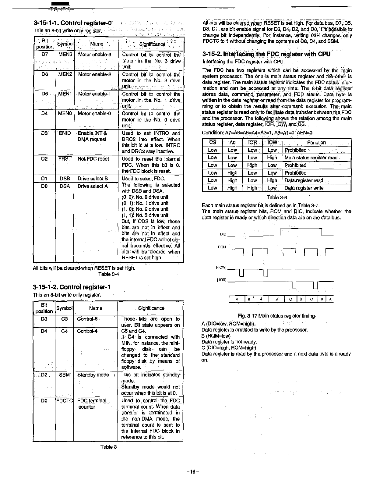
3-15. FDD interface circuit
Tho FDD intorface circuit supports two floppy disk units at a maximum. Fig. 3-16 shows the block diagram. A TC8566F floppy disk
controller
is
used
to
interface
the
floppy
disk
units
with
the
CPU.
FDC
NOTE: The 74HC157 is used to select between the built-in 3.5 inch
FDD and optional 5.25 inch FDD for drive A in the set-up
menu.
Fig. 3-16 FDD interface block diagram
3-15-1. TC8566F floppy disk controller
The TC8566F floppy disk controller contains a VFO and peripheral
logic
circuit
on a single
chip.
Two
control
registers,
main
status
register,
and
data
register
are
on
the
chip.
Table 3-3
shows
the
relation
between
address
line
and
registers.
AEN
~
A7
A6
A5
A4
A3 A2
A1
AO
Function
H
X
X X X X
X
X
X
X
X
H
X X X X
X
X X X
X
X
L X X X
X
X X X
X
X
X
L
X X
X
X
X
X
No
selection
X X
X
X
L
X X X X
X
X X
X
X
X
L X X X X
X X X X X X H X X X
L
L
H
H
H
H L
L L
L
L
L H
H
H L L L H
Prohibit
H
L
L
H
H
H
H
L
L H L
Conlrol
regisler-O
L
L
H
H
H
H L
L H
H
Control
register-1
L
L
H
H
H
H L H L L
Main
status
register
L L H H H H
L
H
L
H
Data
register
L
L
H
H
H
H L H H L
No
selection
L L H H H H
L
H
H
H
Table 3-3
-,
~--~------------------~~-------------------
3·15.1~1.
Confrorregister-O
This
an
8~bit
write onl)ilegisfer .
.:
.'
,
-r'
iSit
",.
,.
" _
Si9fl'ific~lIice~
: position
Syinpol
:
Name
.
.""
.
07
MEN3
Motor enable-3
Control
bit
to
control
the'
"'.
-~
-
lJ'lotqr
in:
the
NO. 3 ..
<lrive
,
.'
,
vnit.
':
,
06
MEN2
Motor enable-2
Control
bif
io
""nttol the
motor
in
the
No.2
drive
.::.
:unit.:~:
-
,>
-
,
..
. OS.
. ,
MEN1
Motor
ena~l.e-1
C_ontrol
bit
to
contr91-
the
.~~9.~r~j~~.~~e:...
N~.
,1
___
~ri.,,~.
unit - :
:
04
MENO
Motor
enable-O
Control bit to
control
the
motor
in
the
No. o
drive
- . ,
unit
03
ENIO
EnablelNT &
Used
to
set
INTRO
and
OMA
request
CRGl2
into effect
When
this bit
is
ai a
low.
INTRO
and
ORQ2
stay
inaCtive.
02
FRS!
Not
FOC
reset
User::!
to
reset
trie
internal
FOC.
When
this
bit
is
0,
the
foe
block
is:
reset.
01
OSS
Drive
select
B
Used
to select
FOC.
00
OSA
Drive
select
A
~~~;6~~::
O~A~elected
(0,0):
No. 0 drive
unit
(0,1): No.1
drive
unit
(1,
0):
No.2
drive
unit
(1, 1): No.3
drive
unit
Sut,
if
COS
is
low,
those
bits
are
,not
in
'effect
and
bits
a'ra
'riot
-in
effect
and
the
.internal.
FOC
select
sig-
nal
becomes
effective:
All
bits'
will
be
'Cleared
when
RESET
is set
high.
All
bits will
be
cleared when
RESET
is
set
high.
Table
3-4
3-15-1-2.
Control
register-1
This
an
a-bit
write
only
regi$t~r.
Sit
Symbol
Name
position
03
63
Control-5
04
C4
Control-4
.
:02·.'
SSM
Standby
mode
PO
FOCTC
POC
letlllin,!! .
Sighificance
These -bits
are
open
to
u&er
•.
Bit
stat!3
appears
on
CS
and
C4
..
If
C4
is
connected
with
MIN,
for
instance,
the
mini-
floppy disk
can
be
changed
to'
the
standard
floppy ·disk by
ineans
of
sqftware.
This
bit
indicat~s
standby
mode~
'I.
-Standby mode.
would
not
oCc_ur
Wht;ln
thi~
bit
is
at
o.
Used
to.
con.trol
tl\~:'FOC
counter
!
terminal
count.
When
data
transfer
is
terminated
in
the
non-OMA
mode,
the
terminal
count
is
sent
to
the internal
FOC
black
in
reference
to
this
bit.
Table 3
,
-18-
Ailbitswijjbeclear~d
whenRESETis set high.'
FQrodaiabLis~
oI:Os,
D3,
01,
are
bit."able
signallarOl!,
D4;;
OZ,
ana
OO;ifispCissioleto'
change
bit
independeNly.,
For
instanc$,
V(riting,'
03H
changes,
only
FOCTC
to
1 without changing thecantents of
C6,
C4;
and
SSM
..
3-15-2.
Interiflci~gthe
!"pC
register
with
CPU
Interfacing the
FOC
register witli
CPU:
The
FOC
has
two
registers
which
can
be
aoCes~ed'
by
the
main
system
processor.--
The
one
is
main
status,
register
and
the
oth~r
is
data
register.
The
main
status
register
indicates
the
FDC,status-i-nfor-'
mation
and
can
be
_accessed
'at-'any·-'tiltfet.
The-
a-oit
data:-regfster
stores
data,
command;,
:pa-rameter~
-and
-:
FDO
s~atus;-
O~ta,
byte'
is
written
in
the
data
rsgi~t~r-or
re.ad
fr9mths_data
~egister
for
prQg,r~m
'11ing
or
to
obtain
the
re~u!~
after
-command
exec'ulion.
rJl~,
main'
status
register
is
read
only
to
faciJi~~te
d~~
transfer
jjetweeo.UJ,e,
F.OG
and
the
processor.
The
foll9,Wh'J9
shows
the
relation
,among
the
main
status
register,
data register, IOR,J9W
..
and.CS.
Condition:
A7=A6=A5=A4=A2=1,
A3~A1
=0,'
AEN=O
CS
AO
1Ol'f
i5W
_
Function.
Low
Low
LaW
.L,ow
Prohil;>ited
. .
.'.
Low
Low
Low
High
Main
status
register
read
Low
Low
High
Low
prohibited
Low
High
Low
Lqw
Prohibited
Low
High
Low . High
Data.register
read
Low
High
High:
L,o,w
,
D~.ta
register
write
Table
3-6
Each
main
status
register
bit
is
defined
as
in
Table
3-7.
The
main
staJusregister
bits,
ROM
and
010,
indicate
whether the
data
register
is
ready
or.Yihich
direction
data
are
on
the
data
bus.
DIO
__
-'-
____
-'
ROM
[oIOWJ-u
u
[.IOR]
________
,
r---,
Fig.
3-17
Main
status
register timing
A (0I0=low,
ROM=high):
Data
register
is
enabled
to
write
by
the
processor.
S
(ROM=low)
Data
register
is
not
ready.
C
(OIO=high,
ROM=high)
L
Data
register
is
read
by
the.
processor
and a next
data
byte
is
already
on .
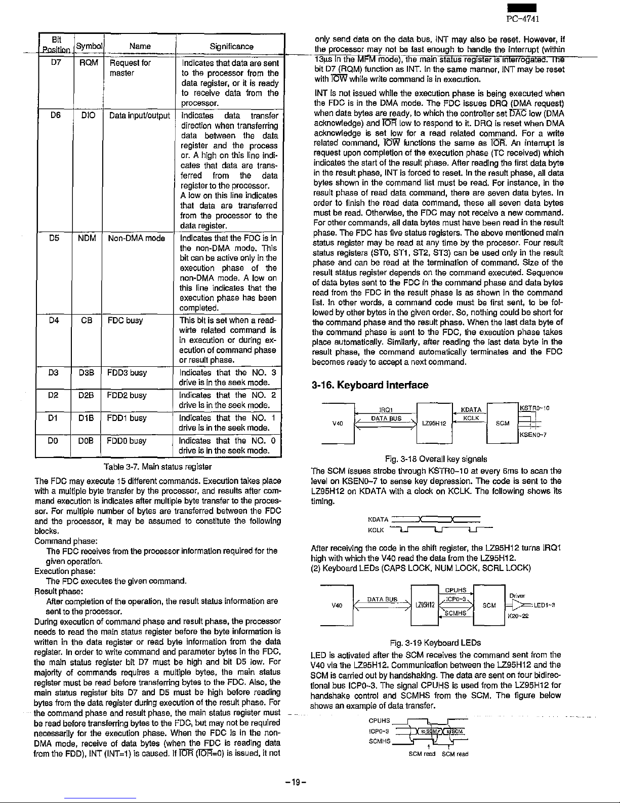
Bit
I Position
Symbol Name
Significance
D7
ROM
Request
for
Indicates that data
are
sent
master
to the processor from the
data register,
or
it is ready
to
receive
data
from
the
processor.
D6
DIO Data inpuVoutput
Indicates
data transfer
direction
when
transferring
data
between
the
data
register
and
the
process
or.
A
high
on
this
line
indi-
cates that data are transferred
from
the data
register
to
the processor.
A
Iowan
this line indicates
that
data
are
transferred
from the processor to the
data register.
DS
NDM Non-DMA mode Indicates that the
FOC
is
in
the
non-DMA mode. This
bit
can
be
active
only
in
the
execution
phase
of
the
non-DMA
mode. A Iowan
this line indicates that the
execution phase has been
completed.
D4 CB FDC busy
This bit is set
when a read-
wirte related command is
in
execution or during ex-
ecution
of
command phase
or
result phase.
D3 D3B
FDD3 busy Indicates that the NO. 3
drive is
in
the seek mode.
D2 D2B
FDD2 busy Indicates that the NO. 2
drive is in the seek mode.
D1
D1B
FDD1
busy
Indicates that the NO. 1
drive is in the seek mode.
DO
DOB
FDDO
busy Indicates that the NO. 0
drive is in the seek mode.
Table 3
R
7.
Main status register
The FOC may execute 15 different commands. Execution takes place
with a multiple byte transfer by the processor, and results after com
R
mand execution is indicates after multiple byte transfer to the proces
R
sor. For multiple number of bytes are transferred between the
FOG
and the processor, it may be assumed to constitute the following
blocks.
Command phase:
The FOC receives from the processor information required for the
given operation.
Execution phase:
The
FOG
executes the given command.
Result phase:
After completion of the operation, the result status information are
sent to the processor.
During execution
of
command phase and result phase, the processor
needs to read the main status register before the byte information is
written in the data register or read byte information from the data
register.
In
order to write command and parameter bytes in the FOC,
the main status register bit
07
must be high and bit
05
low. For
majority
of
commands requires a multiple bytes, the main status
register must
be
read before transferring bytes to the
FOG.
Also, the
main status register bits
07
and
05
must be high before reading
bytes from the data register during execution of the result phase. For
the command phase and result phase, the main status register must
be read before transferring bytes to the FOC, but may not be required
necessarily for the execution phase. When the
FOe
is in the non-
OMA mode, receive of data bytes (when the
FOe
is reading data
from the
FDD),INT
(INT=1) is caused.lfTOl'i (lOR=O) is issued,
it
not
-19-
-
PC-4741
only send data on the data bus, tNT may also be reset. However,
if
the processor may not
be
fast enough
to
handle the interrupt (within
13J.lS
in
the MFM
m6C9}~e
main status register IS Interrogated. I
he
bit
07
(RQM) function as INT.
In
the same manner, tNT
may
be reset
with
iOW
while write command is in execution.
INT is
not
issued while the execution phase is being executed when
the FDC is
in
the DMA mode. The FDC issues DRO (DMA request)
when data bytes are ready, to which the controller set
Ii7iC
low (DMA
acknowledge) and
TOR'
low to respond to it. ORQ is reset when OMA
acknowledge is set low for a read related command. For a write
related command,
TOW
functions the same as
~.
An
interrupt is
request upon completion
of
the execution phase
(Te
received) which
indicates the start of the result phase. After reading the first data byte
in
the result phase, INT is forced to reset. In the result phase, all data
bytes shown
in
the command list must be read. For instance, in the
result phase of read data command, there are seven data bytes. In
order to finish the read data command, these all seven data bytes
must be read. Otherwise, the FOC
may
not receive a new command.
For other commands, all data bytes must have been read in the result
phase. The FOC has five status registers. The above mentioned main
status register may be read at any time
by
the procesor. Four result
status registers
(STO,
8T1, ST2, ST3) can be used only in the result
phase and can be read at the termination
of
command. Size of the
result status register depends on the command executed. Sequence
of
data bytes sent to the FDG
in
the command phase and data bytes
read from the FOC
in
the result phase is as shown in the command
list. In other words, a command code must be first sent,
to
be fol-
lowed
by
other bytes
in
the given order. So, nothing could
be
short for
the command phase and the result phase. When the last data byte
of
the command phase is sent to the FDG, the execution phase takes
place automatically. Similarly, after reading the last data byte in the
result phase, the command automatically terminates and the FOC
becomes ready to accept a next command.
3-16.
Keyboard i nleriace
IRQl
KDATA
~
DATA
BUS
KCLK
V40
LZ95H12 SCM
KSENO~
10
Fig. 3-18 Overall key signals
The SCM issues strobe through KSTRO-1 0 at every 6ms to scan the
level on KSENO-7 to sense key depression. The code is sent to the
LZ9SH12 on KDATA with a clock on KCLK. The following shows its
timing.
KDATA
:=:::=::x::==x=
KCLK~
After receiving the code
in
the shift register, the LZ95H12 turns IRQ1
high with which the V40 read the data from the LZ9SH12.
(2)
Keyboard LEDs (CAPS LOCK, NUM LOCK, SCRL LOCK)
,-
CPUHS
DATA BUS
ICPO-3
D~ver
V40
Llg5H12
SCM
>=
SCMHS
K~~22
LE01~3
L--
Fig. 3-19 Keyboard LEDs
LED is activated after the SCM receives the command sent from the
V40 via the LZ9SH12. Communication between the LZ9SH12 and the
SCM is carried out by handshaking. The data are sent on four bidirectional bus ICPO-3. The signal CPUHS is used from
the
LZ9SH12 for
handshake control and SCMHS from the SCM. The figure below
shows an example of data transfer.
CPUHS~
ICPO-3
to
S M t
SCM
SCMHS
1
SCM
read
SCM
read
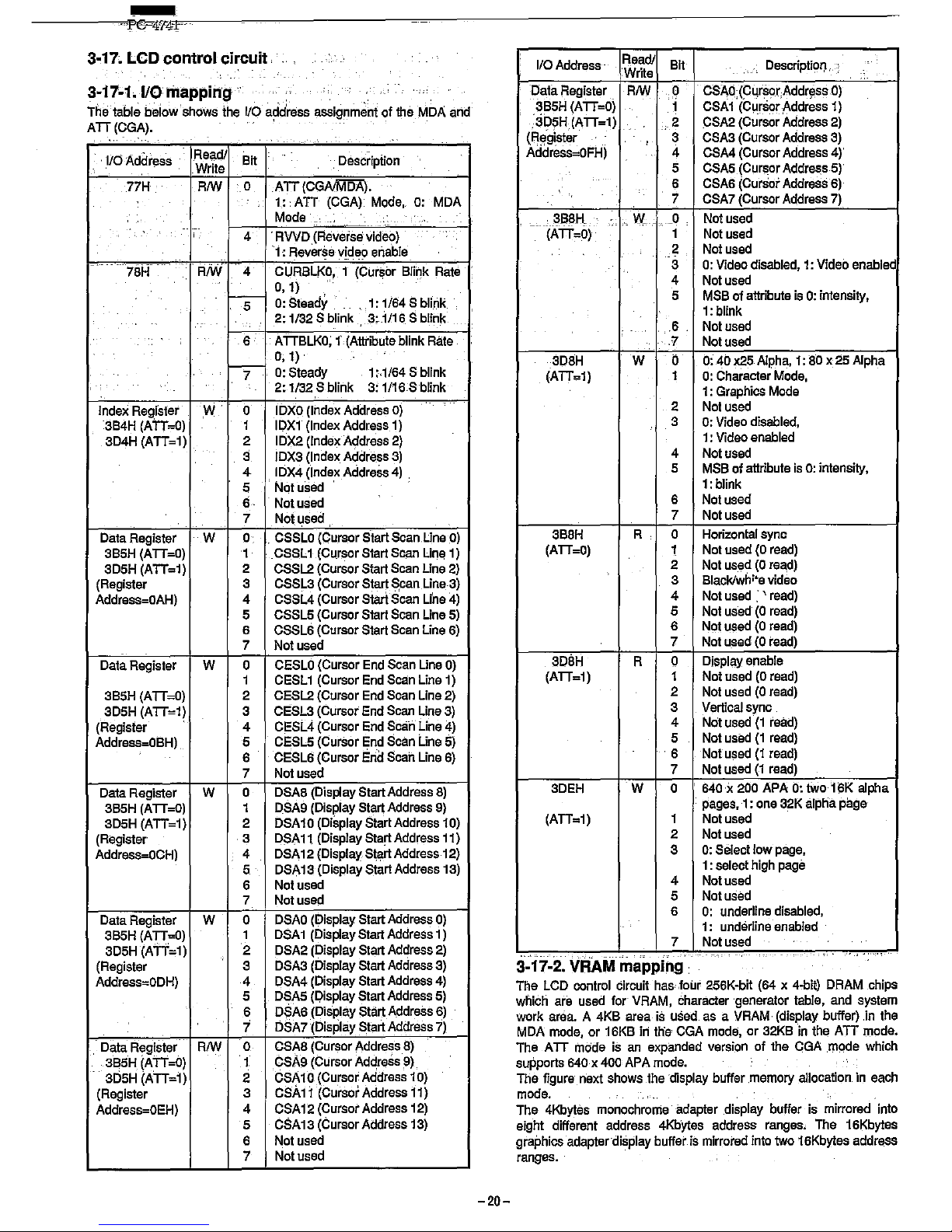
-
3-17,
LCD
control
circuit
3-17-1.
1/0
mapping
"
The table beiow'shows the I/O address assignment
of
the MDA and
ATI(CGA).
'
I ' , I/O Address
Readl
Bit
Description
Write
77H RIW
0
ATT
(CGAIMDA).
1:
ATI
(CGA) Mode,
0: MDA
Mode _
_.
--
4 .
RWD
(Reverse video)
1
~
F:!ever$e
vi~~!l
enable
,
78H
'RJW
.
4
CURBLKO, t
(Cilr~or
BIi~k
Rate
0,1)
,
S-
,
0: Steady
,1:1/64Sblink
,','
,
'
",
2: 1/32 S blink
3:
1116,
S blink
6 A TIBLKO,
t.
(Attribute blink Rate
f--]
a, 1) ,
0:
Steady
1
:,1/64
S blink
,',
2:
1132
S blink
3:
1/16S blink
Index
Register
W
0
IDXO
(Index Address 0)
3B4H (A
TT
=0)
1
IDXl
(Index Address 1)
3D4H
(ATT=I)
2 IDX2 (Index Address 2)
:l
IDX3 (Index Address 3)
4 IDX4 (Index Addre
..
4)
,
5
Not
used
'
6
Not
used
7 Not,used
Data Register
W
0 . CSSLO (Cursor Start Scan Line 0)
3B5H (ATI=O) 1 CSSL 1 (Cursor Start Scan Line 1)
3D5H
(ATI=I)
2 CSSL2 (Cursor Start Scan Line 2)
{Register
3 CSSL3 (Cursor Start Scan Line 3)
Address=OAH)
4 CSSL4 (Cursor Start Scan Une
4)
5
CSSL5 (Cursor Start Scan Line 5)
6 CSSL6 (Cursor Start Scan Line 6)
7
Not
used
Data Register
W 0
CESLO (Cursor End Scan Line 0)
1 CESL1 (Cursor End Scan Line 1)
3B5H (A
TT
=0)
2 CESL2 (Cursor End Scan Line 2)
3D5H
(ATI=I)
3
CESL3 (Cursor End Scan Line 3)
(Register
4
CESL4 (Cursor End Scah Line
4)
Address=OBH)
5
CESL5 (Cursor End Scan Line 5)
6
CESL6 (Cursor End Scan Line 6)
7 Not used
Data
Register
W
0
DSA8 (Display Start Address 8)
3B5H (ATI=O)
1 DSA9 (Display Start Address 9)
3D5H
(ATT=I)
2
DSA 10 (Display Start Address 10)
(Register
3
DSA 1 t (Display Start Address 11)
Address=OCH)
4
DSA 12 (Display Start Address 12)
5
DSA 13 (Display Start Address 13)
6
Not
used
7
Not
used
Data
Register
W 0
DSAO
(Display Start Address 0)
3B5H(ATI=0)
1
DSA 1 (Display Start Address 1)
3D5H
(ATT=I)
2
DSA2 (Display Start Address 2)
(Register
3
DSA3 (Display Start Address 3)
Address=ODH)
4
DSA4 (Display Start Address
4)
5
DSA5 (Display Start Address 5)
6
DSA6 (DiSplay Start Address 6)
1
bSA7
(Display Start Address 7)
Data
Rf!!gister
RIW
a
CSA8 (Cursor Address 8)
3B5H (ATI=O)
1
csAs
(Cursor Address 9)
3D5H
(ATT=I)
2
CSA 10 (Cursor Address 10)
(Register
3
csA
11
(Cursor Address 11)
Address=OEH)
4
CSA 12 (Cursor Address 12)
5
CSA 13 (Cursor Address 13)
6 Not used
7
Not used
-20-
I/O Address'
Read!
Bit
,.;
Descriptiory, ,
Wrtte
Data Register RIW 0
CSAO,(CuiSorAddr~ss
0)
SB5H
(A
TT
=0) 1 CSA 1 (Cursor ,Address 1)
3D5H(ATI=t)
2 CSA2 (Cursor Address 2)
(Register
,
3
CSA3 (Cursor Address 3)
Address=OFH) 4 CSA4 (Cursor Address
4)
5 CSA5 (Cursor Address 5)
6 CSA6 (Cursor Address 6)
7 CSA7 (Cursor Address 7)
----
3B8H,
..
W
0,
Not used
(ATI=O)
1 Not used
2,
Not used
3 0: Video disabled, 1: Video enabled
4
Not used
5 MSB
of
attribute
is
0: intensity,
1: blink
.,
.6
, Not used
,7
Not used
3D8H
W 0
0: 40
X25
Alpha, 1: 80 x 25 Alpha
(ATI=I)
1 0: Character Mode,
1: Graphics Mode
2 Nol used
3 0: Video disabled,
1: Video enabled
4 Not used
5 MSB
of
attribute
is
0: intensity,
1: blink
6 Not used
7
Not used
3B8H
R
a
Horizontal
sync
(ATI=O) 1
Not used (0 read)
2 Not used (0
re~d)
3
Blacklwhj"e
video
4
Not
used
: '
read)
5 Not used (0 read)
6 Not used
(O
read)
7 Not used (0 read)
3DBH R
a Display enable
(ATI=I)
1 Not used (0 read)
2 Not used (0 read)
3 Vertical sync
4 Not used
(1
read)
5
Not used
(1
read)
6
Not
used
(1
read)
7
Not used
(I
read)
3DEH
W 0
'
640
x 200 APA 0:
!wolaK
alpha
pages, 1: one 32K alpha page
(ATI=I)
1 Not used
2
Not used
3
0: Select
low
page,
1 : select high page
4 Not used
5
Not
used
6 0: underline disabled,
1:
underline
enabled
7 Not used
....
_.,
3-17-2. VRAM
mapping
The LCD control circuit
has,
,foilr 256K-bit (64 x 4·bit) DRAM chips
which
are
used
for
VRAM,
character
'generator
table,
and
system
work area. A 4KB area is used as a VRAM (display buffer).in the
MDA mode,
or
16KB hi
th'.
CGA mode,
or
32KB
in
the
ATI
mode.
The A
TI
mode is an expanded version
of
the CGA ,mode which
supports
640
x 400 APA mode.
The figure next shows the display buffer memory allocation in each
mode.
The 4Kbytes monochrome
ad~ter
display buffer is mirrored into
eight different address 4Kbytes address ranges. The 16Kbytes
graphics
ad~terdisplay
buffer is mirrored into two 16Kbytes addre
..
ranges.
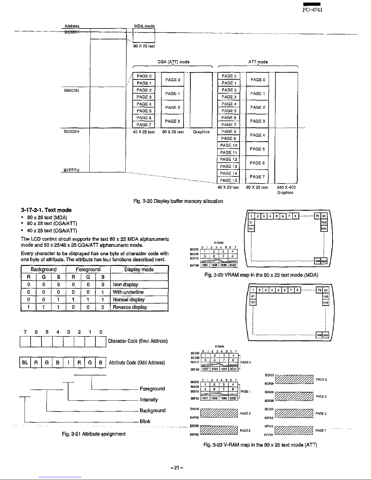
Add
ress
8Qoooti
jMDAmOd'1
80 X 25 taxt
-
PC-4741
eGA
(A
JT)
mode A
TT
mode
r---
________
~LC~
________
~,
,r-------------'~~~--------,
--
PAGE 0
PAGE 0
PAGE 1
8aOOOH
PAGE 2
PAGE 3
PAGE 1
PAGE 4
PAGE 2
PAGE 5
PAGE 6
PAGE 3
PAGE 7
--
BCOOOH
40 X
25
text 80 X 25 text Graphics
BFFFFH
......
-----.
---
--
.
PAGE 0
PAGE 0
PAGE 1
---
PAGE 2
PAGE 1
PAGE 3
---
PAGE 4
PAGE 2
PAGE 5
PAGE
6
PAGE
3
PAGE
7
--
PAGE
8
PAGE
4
PAGE
9
PAGE
10
PAGE
5
PAGE
11
--
PAGE
12
PAGE 13
PAGE
6
--
PAGE
14
PAGElS"
PAGE?
--
40 X 25 text 80 X 25
text
--
640 X
400
Graphics
Fig_
3-20 Display buffer
memory
allocation
3-17-2-1_
Text
mode
80 x 25
text
(MDA)
•
80 x 25
text
(CGAlATT)
•
40 x 25
text
(CGAlATT)
The LCD control circuit supports the text 80 x 25 MDA alphanumeric
mode
and
80
x 25/40 x
25
CGAlATT
alphanumeric
mode.
Every character to be displayed has one byte of character code with
one
byte
of
attribute.
The
attribute
has
four functions described
next.
Background
Foreground
Display
mode
R
G B R G B
0 0
0
0
0 0
Non
display
0 0
0
0 0
1
With underline
0
0 1 1 1 1
Normal
display
1 1
1
0
0 0
Reverse
display
7 6 5 4 3 2 0
I
Character
Code
(Even
Address)
I
BL
I
R
G
B R G B
Attribute
Code
(Odd
Address)
T
Foreground
I
T
Intensity
Background
Blink
fig,
~-g1
At1riQl,!t_~
~~signment
-21-
V-RAM
1
213
14
15
16
17 18
~-
.....
-."
"
81
160
t;-;;
0
T
~----
... -...
-.---
..
--.--
..
-----.-
..
-~
Fig.
3-22
VRAM
map
in
the
80 x 25
text mode
(MDA)
1
213
14
1 5
16
17
la
t········~~
~
~
V-RAM
eo"",
4
00000
~"i'~'i'~4~5~5~'~
B0010
PAGE
0
BSF98
1997
1998
1999
2000
BIl000012~4567
BO008
00010
B8F9B
,
5
1997
,
,
4
5
,
8
1998
1999
2000
PAGEl
BaOOO
--
~PAGE3
SBF9B
-.--.--
......
--------
...
--.--------~J
BCGOO
~PAGE4
BCF9B
BDOOO~
f'l'//////////////.l
PAGE
5
BDF9S
rL<:LL.CL.o'LLu,=""
BEOOO~
V//////////////1
PAGE
6
BEF9B
U,CUO:LL.li.<OLLLLoW
BFOOO~
V//////////////1
PAGE7
BFF9B
""'LL<L.<'LLLLCUOZod
Fig.
3-23
V-RAM
map
in
the
80 x 25
text
mode
(ATT)
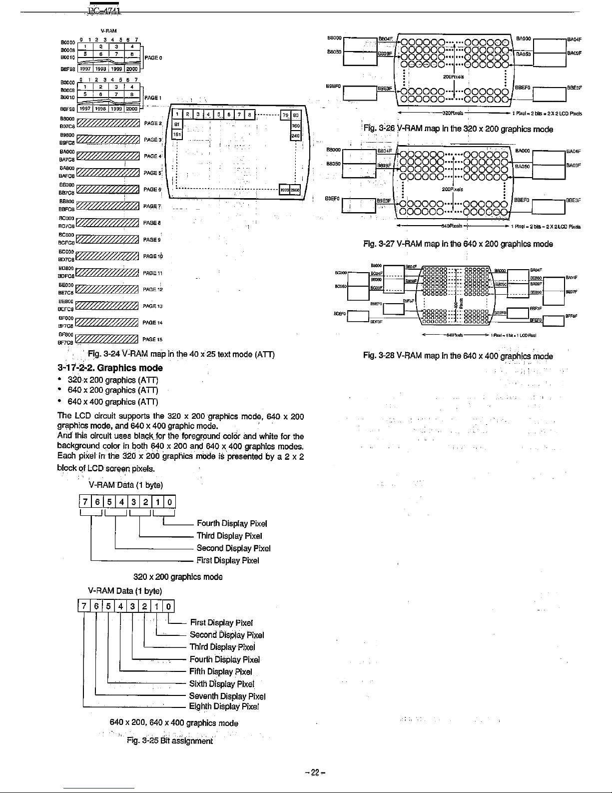
.~
------~.~~~-----------------------------------------------------------
V-RAM
BOOOO
, , ,
3 4
5 ,
7
80008
,
3
80010
7
,
PAGED
'"''
1997 1998 1999
""
80000
, , ,
3
4
5 ,
7
BOO08
,
3
"""
7
,
PAGEl
Bef98 1997 1998 1999 2000
::~~:W~//40//1
PAGE
2,
::~:f7#/#/#//!//;l
PAGE
3:
~~~~V/#ff/$//M
PAGE4
=~~@"~&
PAGE~:
::~~V/m~A
PAGES;
BSaOO
.
88FC8~/#4J
PA!'i.E?
:~~:W&/W~//1
PAGE8
:~:::~W//$/%///A
PAGES:
:~;~:~4J
PAGE10
:~::W/07#ffiW&
PAGEll
::~~
Vm;wffi'//#//J
PAGE
12
:::~:
W/ffi'//0//
ff!g
PAGE
13
::;~~I0000W/ffA
PAGE14
:~:~@#/ffM
PAGElS
1 2
3
4_
5
•.
6 7 8
--------
79,
80
81
160 ,
161
240 '
~
~----------·-·-~-----J~~-'--:--i-------~:
Fig.
3-24
V:RAM
map
in
the
40
x25
text
mode
(AIT)
3~11~2·2.
Graphics mode
320 x 200
graphics
(A
IT)
•
640 x 200
graphics
(A
IT)
•
640 x 400
graphics
(A
IT)
The
LCD
circuit
supports
the
320 x 200
grapliics
made,
640 x 200
graphics
made,
and
640 x 400
graphic
made.
J
And
this
circuit
uaeS
bla~K
for
the
f9regrpund
calor
and
white
far
the
background
color
in
both
640 x 200
and
640
x.
400
graphics
modes.
Each
pi*el
in
the
320 x 200
graphics
mode
is
presented
by
a 2 x 2
black
qf
LCD
scr~en
pixels.
V-RAM
Dala
(I
byte)
1*15141*11101
t
y
y~
Fourth
Display
Pixel
I I
L
_____
Third
Display
Pixel
'-------
Second
Display
Pixel
'----------
First
Display
Pixel
320 x 200
graphics
mode
V-RAM
Data
(I
byte)
17161514131211101
I
First
Display
Pixel
Second
Display
Pixel
Third
Display
Pixei
Fourth
Display
Pixel
Fifth
Display
Pixel
Sixth
rJisplay
Pixel
Seventh
Display
Pixel
Eighth
Display
Pixel
640 x 200,
640 x 400
graphics
mode
Fig_
3'-.25
Sit
assignment
"""
r--:-~"~04!C'-kXO~O)OO<O)OQ..::
..
~.::
..
CO)(OXO)(OJcO)(o)1-
8AOOO
,---,BA04'
t
=j!l!9.!E.r·so:OOOOO'''!'''OOOOO.0i"iiiii<,-I-----I
S80SO
S80SF
.
00000'"
...
ooood~
BAOSO
BA09F
9°080°'"
···qOOOO.c.>-t--L
__
---1
: ' 200Plxels ' :
B9EFO
r--]!''!!9E3~'+<.;.,J:
00000
... 1
...
000006
BBEFO
.----,
rBBE3F
000000·"
'''OOOOOot~---L-
__
-I
320Plxels
1
Pixel
.. 2
bils"
2X 2
LCD
Pblels
'FIg.
3-26
V-RAM
map
in
the
320 x 200
graphics
mode
"'00
r-:-....'...=·~~~·
,~,,'-i<;;:.
;Co;;:;::-~~~~.~.~.~.
~
SAOOO
.--~
SAO"
.
00000
.. · '''000000
"",
r·-~
.~"~"!E.FJ;'~088888:::1:::888880X"£;?"hBA"""'50;l--~
"""
'9.00000'" ·
..
OOOOOI(.>+--l.
__
---.J
:
2COPixels
:
B""
r-,--~··"]!B~"'!E.'.\o',6,.;:
b,·
0000"')'''000006
,
·1'
~.
o~o~o~ogo~o~
..
;.
';"'O~.
~o~o~.o~o~,
?t,=~~
.:
640Plxels 1 Plxel_2bits_2X2LCDPixels
BBEFO
.--~
BBE3F
Fig.
3-27
V-RAM
map
in
the
640 x 200
graphics
mode
~.1s_1Ax.I~lhit.1LCOAIc.1
Fig.
3-28
V-FjAM
map
in
the
640 x 400
graphi?"
mode
-22-

CHAPTER
4.
LCD UNIT
-
PC-4741
For the scan start signal S has been transferred at the first line to
display the data by the combination
of
the LCD scan electrode and
----------------------~tI~jensmly~I~lal~~d~lt.ta~g~er..-----------------------------
While the first line data are being displayed, the second line display
4-1. Structure
A 640 x 400 full dot graphics display unit
is
employed for the
LCD
unit
which consists of a printed circuit board that contains the LCD panel
and its electronic
cirCUits,
an
electrically connected film carrier LSI
chip, and a mechanically held plastic chassis, and a bezel.
4-2. Operational theory
Circuit block diagram and interface signals are shown in the figure
next.
LC
"
DLO'1
~
LeDUO-LeCU3
DUO-3
g~~
CPI
S
Is
II
B-
M 1
I
SEG
drivers
(Upper)
I
L.,
j
40 X 400
LCD
panal-
,
signal generation d.cult
;=
0
0
'M
-
I
SEG
drivers
(Lower)
vee
eND
VLCD
3r
iaS
voltsgaI
generation
circuli I
LCDLO-LCOL3
YI
I
CirCUIt
bock
diagram
Interface signals
Pin
NO.
Symbol
Description
1
S Scan start signal
2
CP1
Input data latch signal
3 CP2 Data input clock signal
4 PVBKL Back light power control signal
5 GND Ground
6
VLCD
liqUid crystal drive power
(-)
7
LCDUO
Display data signal (upper
halD
8
LCDU1
"
9 LCDU2 "
10
LCDU3 "
11
LCDLO
Display data signal (lower
halD
12
LCDL1
"
13
LCDL2
"
14 LCDL3
"
I
Active
signal
level
nH"
H
....
L
H
....
L
H (ON), L (OFF)
-
-
H(ON), L(OFF)
"
"
"
H(ON), L(OFF)
"
"
"
The display screen of this unit
is
configured of 640 x 400 dots two
screens, each screen driven with 1/200 duty.
An
BO-pin
LSI
is
used for the
LCD
driver that consists of a shift
register, latch, and LCD drive circuit.
Data are inputted for each line (640 dots) of the screen. From the left
side of the screen, 4-bit parallel data
are
sent one at a time via the
shift register with the clock pulse CP2. When the 640 dots data have
been received for one display line, the data are latched as a parallel
data with respect
to
the 640 signal electrodes at a high to low transi-
tion of the latch signal
CP1
to send the drive signal by the drive circuit
to the corresponding electrodes.
-23-
data are received. Upon completing transfer of 640 data, it will then
be latch at a high
to
low transition
of
CP1
to change it to display the
second line.
In
this way, data input are repeated to the 200th line from top
to
bottom using the multiplexed method. After completion
of
one screen
(one frame), data are then received from the first line again. The scan
start signal S
is
the scan signal
to
drive horizontal electrode.
For it causes the liquid crystal elements to deteriorate because of
chemical reaction if
DC
voltage
is
added to the LCD panel, the drive
signal waveform must be inverted at every screen
in
order to avoid
generation of
DC
voltage. The circuit employed
to
do this is the async
M signal circuit from which generated the drive waveform AC signal
M.
Because of the characteristics of the CMOS driver LSI, power consumption increases as CP2 clock frequency increases. Therefore, it
incorporates four
sh~ft
registers to transfer the 4-bit parallel data via
these shift registers
to
decrease the CP2 clock data transfer speed.
In
this circuit, a 4-bit display data
(LCDUO
- 3 for upper half screen and
LCDLO
- 3
for
lower half screen) are supplied through the data input
lines.
To further abate the power consumption, it also has a data input bus
line system which comes operating only when appropriate data are
received.
The following shows the screens signal electrode data inputs vs.
driver
LSI
chip select signal.
The driver
LSI
of the left
end
screen is first elected. When the
SO-dot
data (20CP2) has been supplied, the driver LSI adjacent
to
right is
then selected. This continues until the data are sent
to
the driver LSI
at the screen right.
This process occurs Simultaneously for signal electrode signal LSls
of
both screens.
In
this manner, data of both screens are supplied via
4-bit bus line starting from the left end
of
the screen.
For the graphics display unit does not contain the refresh RAM, it
becomes necessary to input the data and timing pulse when the
screen
is
still.
The following shows the dot table
of
the display, data input timing
chart, and input signal timing.
ldot
2dol
3dot
20Odot
201dot
40Odol
ldol
,,'"
3dot
64Qdot
,
.,
,
."
t
.,
-----
........ --..
----
....
---
...
---
..
~
".
,
,
."
.~
.~
S
~
~
~
•••••••••
u
•••••••
uuuuuuu
•••••••••••••••••••••
i400.640j
NOTE: 1
aoo21ndicale
li'Sl
horizontal
dol
and
sec:OnddoL
Olsplil)'
dOlchart.
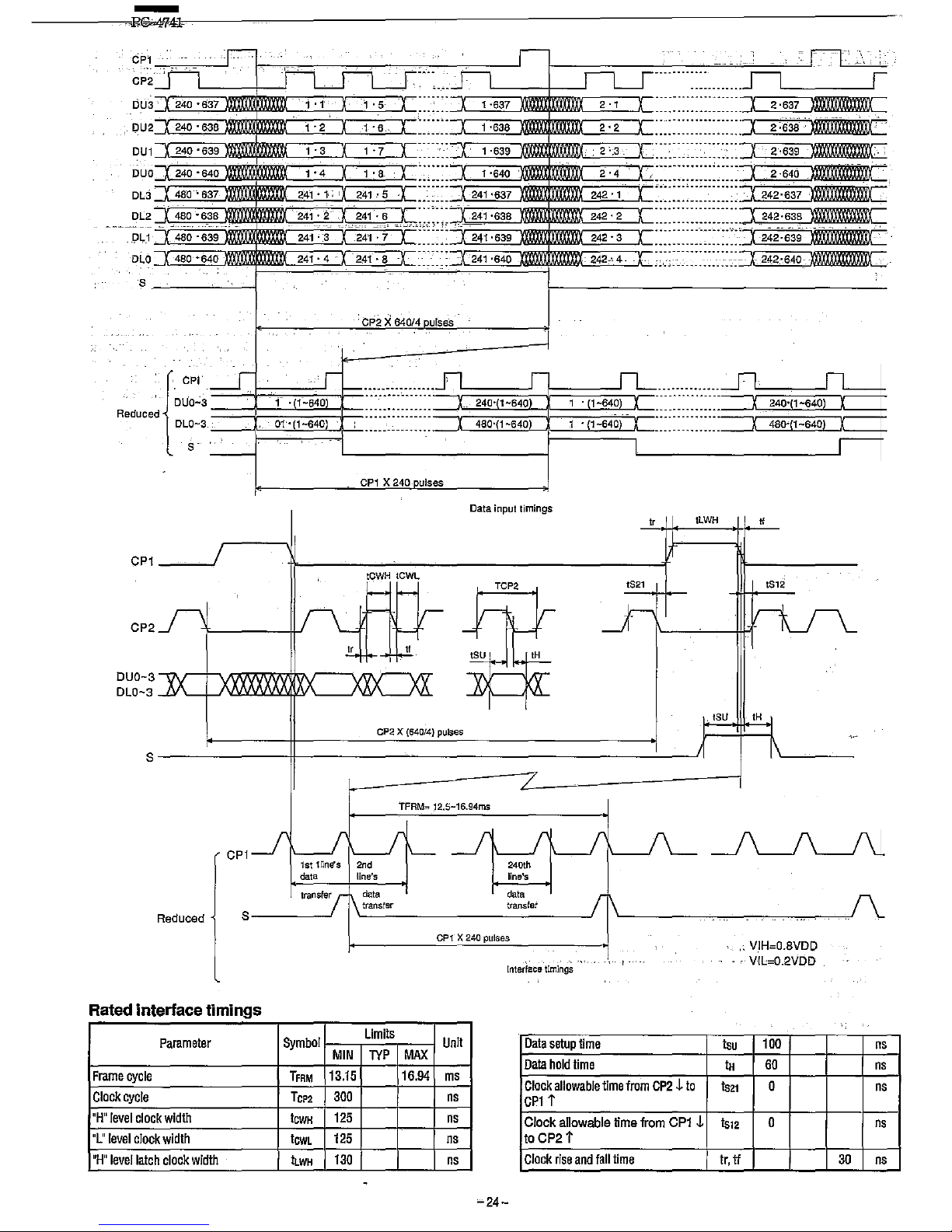
-
CP1
.... 'r-:
.'
I
..
:
~
,'"
',\':-
,
cP~'~
~"'~.F1
----
JLS
........
::::
........
~
DU3
240 -6'37
1 ' 1
DU2
240'
638
1
-2
DU1
240 "639
1
-3
X
_DUO
240
-640
l'
4
DL3
480
-.
637
241'
1 ..
DL2
480
-638
241'
2-
PL1
480
'639
241'
,3
DLO
480-~640
241'
4
S
.
CP1_~~
CP2
OUO-3
\!V-+,\/liW"","WrJ\/
OLO-3
1 '
5
X
1 -637
1 •
6,
X X
1 -638
1
-7
X
1 '639
1 ' 8
X X
1 -640
241-"5
,I
-X
241'637
241·
6
X
241-638
,',-,-"
.
241
·7
J...
~241'639
241·
8
X
241
'640
t;P2
X 640/4
purses
CP1
X 240-pulses
Data
input
timings
tCWH tCWL
Tep2
CP2 X (640/4)
pulses
2'1
X
:::::::::::::::::::::J
2,637
~
2'2
X
::.:::::::::::::::::J
2;638lf1iJfJfuij£
.
2'3
X
:::::::::::::::::::::J
2'639
'(jIIJJj'l/J,ijOOC
2-4
X:
:::::::::::::::::::::J
2640
'ftIJ'JJJJfJ.~OOC
242'
1 X
:::::::::::::::::::::J
242'637
'l@'itI1I,ijOOC
242'
2 X
::::::::::::::::::::J
242-638
'@'f$tI:f:!'fJ,'IftC
242'3
X
:::::::::::::::::::'J242:639
-E
tLWH
•
ISU
tH
8----------~~--------~--------------------~~
CP'
Reduced
8----...J
Rated interface timings
Parameter
Symbol
Limits
MIN
lYP
Frame
cycle
TFRM
13,15
Clock
cycle
Tep2
300
"H"
level
clock
width
tOWH
125
"L"
level
clock
width
tCWL
125
"H"
level
latch
clock
width
kWH
130
TFRM=
~2.5-16.94ms
MAX
16,94
240th
line's
do
..
transfer
CPt X
240
pulses
Interface'timlngs
-,-.
Unit
Data
setup
time
Data
hold
time
ms
Clock
allowable
time
from
CP2 ~ to
ns
CPU
ns
Clock
allowable
time
from
CP1
~
ns
to
CP2
t
ns
Clock
rise
and
fall
time
~24-
, VIH=O.8VOD
..
Vil=O,2VOD
tsu
100
tH
60
tS21
0
1s'2
0
tr,
If
ns
ns
ns
ns
30
ns
 Loading...