

Page 1
PC-2500
SHARP
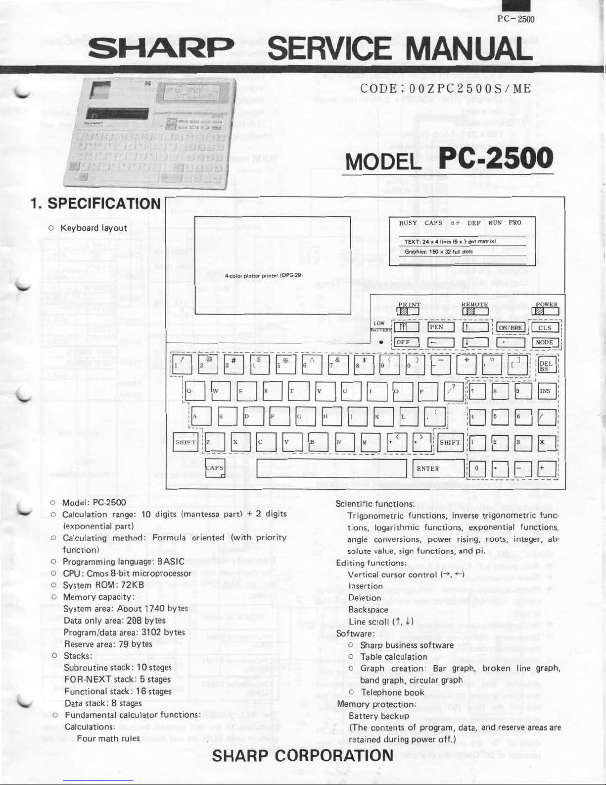
1. SPECIFICATION
o Keyboard
layout
1
0-~
:
1
2 3 4 5
SERVICE
4
-col
or plotter printer (DPG-29
0-rrr:J
)
6
B I:
MANUAL
CODE:OOZPC2500SIME
MODE
~~rn~
7
8
:r~r:JE:JI~Jc:~Jc:J
L
BUSY
TEXT: 24 x 4 lines
Graphics:
PRIN
crn::J
r:-
---------------
[IT[]
I
• : ~
L..:
_______
9
0
PC-250
7:1-t
C
APS
150 x 32 full dots
T
~
E=:J rr=:J
____________
-
DEF RUN
(5 x 7 dot matrix)
RE MO
r:n:::::::J
-,
[I:=:J
TE
________
1
:
I
ON/BRK
L __
___
E=i
0
P
RO
POWER
cra::::::J
..------
Ii~
__ J
I
MODE
:
:
G:J
BS :
~~r
:i
i
I
I
:
:J
o
Model: PC-2500
o Calculation range: 10 di
(exponential
o Ca
lculating
function)
o
Programming
o
CPU: Cmos 8-bit microprocessor
o Syste
o Me
m ROM:
mory
System
Data
only ar
Program/data
Reserve area: 79 bytes
o
Stacks
Subroutine
FOR-NEXT
Functional
Data
stack: 8 stages
o Fun
damental calcul
Calculations
Four math rules
part)
method: Formula
language: BASIC
72KB
capacity:
area: About
ea: 208
area: 3102
:
stack: 10 stages
stack: 5
stack: 16 stages
:
17 40
bytes
stages
ator fu
~--
l
D
EJ
D D
l
o DD DD DD DD
L----,
BiD
gits (mantessa part) + 2 digits
oriented (wi
bytes
bytes
nctions
:
EJ
L------------------------
I
CAP
~
D
I
th pri
orit
D
EJ
y
D
D
---------
EJ
EJ
Scientific
Trigonometric
tions, logarithmic
angle
solute
Edit
ing fu
Vertical cursor control (~.
Insertion
Deletion
Backspace
Line scroll (t
Software
o Sharp business software
o Table calculation
o Graph creation: Bar graph, broken line graph,
o Telephone book
Memory
Battery backup
(The contents
r
etained during power
D
DD
D
CJ
- - ---
functions
conversions, power rising,
valu
nctions
:
band graph, circular graph
protection
LJ!B!D
~
I
I
:
functions, inverse tr
e, sign
:
, .).
)
:
of
LJ~D-trDja
0
1·-- '!o DD
r--
J
ENT
ER
functions, exponential
functions,
+--
program, data, and reserve areas are
off
. )
I
DD I EJ
I
li~DDEJ
t..: _____
___
__ - - - - _ _J
igonometric
roots, i
nteger, ab-
and pi
.
)
D
func-
functions
!
i
'
!
I
i
,
SHARP
CORPORATION
Page 2

PC- 2500
-
Display
:
Liquid crystal display
1.
Text
display
5 x 7 dot
Character size:
Character pi
dot
2. Gr
aphic display
150 x 32 full dots di
Dot
Dot pitch: 0.
Dot si ze:
Printer
:
Printer
type: X and Y axis
P
rint colors: 4 colors
(Op
tion: EA-850C
Charac
ter size: 15 kinds
x 18mm
Minimum pen
Print speed: 7 char
printing with
Recording paper. Paper roll
diameter and 114mm
Pen
moving speed: 73mm/second
tions,
103mm/second
Serial 1/0
Transmission
only
Baud
Parity
Word si
Stop
Connector: 15-pin
devic
e
Output sig
Interfacing signals:
Input
Output
Others
• Auto
•
Power
•
Power
source: 1
in use)
• Rec
o Continuous di
posi
o Intermitte
for
provided
operation
rest of the time (50 min
without
o Printer in operation:
digits
perature
functions
rate: 300,
check: Odd,
ze: 7 or 8 bits
bit: 1 or
nal level: CMOS level (4 ~ 6 volts)
RD, CS,
SD, RS, RR, ER
SG, FG, VC
power off: About 14.5 m
consumption: 6V
supply: Internal recharge
OOVAC, 50.60Hz, with
hargeable battery operating time:
tions (2 rows) under the temp
nt operation: The r
about 1.5
that cal
is
operating the pri
of "5"
of 20°C with
matri
tch: 4.08(W) x 5.44(H) mm (si
space)
size: 0.63 square meter
)
moving di
standard
method: Asynchronous, half-duplex mod
600, 1200 bps
even, n
2 bit
s
connec
CD
splaying: Di
mont
hs,
culator operation or prog
done 10
are pri
nted continuously under the tem-
x display (24
3.35(W) x 4.71
splay
68mm (for both directions
plotting
of
blac
of 0.8mm x 1.2mm ~ 12
stanc
acte
rs/second, max
character
width.
for 45°
one
tor for connection with external
.. ... (DC
splaying
when operated one
min
utes
utes)
nter
.
About
450 digits, provided that 20
the character size
positions x 4 rows)
(H)
mm
s
)
k, blue,
e: 0.2mm
inutes
efreshed
out of one hour with th
green, r
ed
imum (for
si ze "b")
of less than
(Option:
direction
), 6W
able battery (charge
the AC
erature
EA-515P
for X and Y direc
adaptor EA-150
About
"5"
on 48 display
of 20°C.
battery wi
operated to display,
"b".
25mm
)
100 hours
ll last
hour per day
rammed
ngle
mm
o Graph print
described in Page 304 is print
o
Operating temperatur
o
Physical dimensions: 297(W) x 210(D) x 18
front)
o
Weight. About
o
Accessories: Tape recorder interfacing cable, AC adaptor
(EA-150).
red
).
ing: About
e: 5 to 40°
and 45.5 (depth in
1.3kg
write
pen (one each
paper
roll (one
roll), i
11
times,
ed conti
rear) mm
nstruction manual.
when t
nuous
ly.
C
of
black, blue, green, and
he gra
p
(depth in
RAM map
OOOO
H
8KB ROM
internal )
(CPU
2000
H
H
16 KB
R
AM
BASI
4000H
6000H
-
e
7000H
8
000H
FFFF
2.
I
I
I
I
8KB
I
l
Card
I
I
1
card
I
I 8KB
I
I Car
I
I
4KB
RAM
ROM
32
KB
ROM 1
INTER
C
PRETER
TEST
7000
RAM
7200H
image
740
76
RAM
d
7800H
7AOOH
7C
7EOOH
8
PROGR
H
DISP
1
-------
----
DI
SP
2
-------
D!SP 3
-----
DI
SP
-
---
--------
DI
SP
----
----
KEY
-------
KEY
32
ROM
Bund
led software
---
----
4
5
P
ORT
-----
P
ORT
__
KB
-~~K_6_
ROM
2
0H ACK2
00H
OOH
~--- _
000H
AM
-
ACK
--
--
A
CK
ACK
--
ACK 5
1
2
1
3
4
--
Internally implemented memory test program
The
checksum test program ROM is
test the BKB CPU int
RO Ms.
ROM to be tes
CPU
internal ROM
(8KB
)
CPU enternal ROM1
,
e
(32KB)
CPU external RO
(32KB)
The ALL
execution of the test program bec
gram in each ROM are not assured
test.
RESET switch
ted
M2
ernal
ROM and 32KB x 2 external
K
(RUM mode)
CALL&802AI
CALL&8027 I ENT
CA
LL&84F
has
ey ope
91 ENTER
to
contained
ration
ENTER
I
ER
I
I
be
depressed after
ause the
of
data a
its contents after
inte
O
K status
rnally to
11147
10127
38524
the
nd
pro-
the
-2-
Page 3
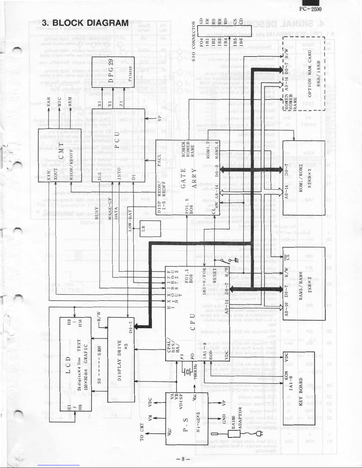
3. BLOCK DIAGRAM
en
C\I
CJ
c,
0
~
u
-
;:;i
::;;
w
0::
-
:><:
-
>
-
N
0::
<
w
0..
...
"
c
...
PC-250
0
-
~
I
.,,.
z
-
z
i:Q
0
0
a,
-
u
0
-
Cf)
-
[;:
C'.J
i:Q
-
cc
i:Q
-
.,,.
i:Q
-
,,,
i:Q
-
so
i:Q
-
,-------,
I
t:s:
r
">,
0::
I
....
• 11
0
•
IQ
.1
::::
'J
I
0
1
<
I
Zi:'l
::;;::;;::;;
1
www
..E'°.£:-:= ___
1
0
0-i::
Q
0::
<
u
;:;i
<
0::
z
0
-
0..
'""
0
__ J
i:Q
::.::
"'
-
<,
i:Q
::.::
<X)
I
I
I
I
I
I
I
I
I
I
I
::i
z
'""
0
-
:><: :><:
I
[-o
:21
u
i...
i...
0
w
0::
<,
z
0
w
0::
Ol
:i::--
0
u
......1
-
:i::-:r:
l
f
"'
:r:
:><:
'""
w
'""
"
"
.,,.
x
fl
"'
"CJ
.,,.
C'.J
<X)
u
-
i...
<
0::
e
u
0
"CJ
C'.J
cc
x
0
~
,,,
-
Q
>
Cf)
::i
i:Q
:::
<,
0::
L
IE--
0
~
Cf)
I
I
I
I
I
C)
Cf)
-
0..
o
I
w
::.::
~
:::i
u
c,
' '
<
<
'""
Q
0
z
'""
-
w
>
-
0::
Q
>
<
....J
0..
Cf)
-
Q
-
Q
<
'""
i:Q
~Hi:Q
....J ....J
I
0
Q
,,,
x
IE--
....J
o
<
0..
'-.
i.,.
z
e,
00
WW
0::0::
O..u>
Cf)
I
--
Q
::;;i:Q
WWW
;:;i;:;i::;;
00
0::0::0::
(J:.l
[-o
<:t:
CJ
,,,
-oo
00
i.,.i:Q
<:
:>-<
0::
0::
<:t:
I
C'.J
.,;
-
::;;
0
0:: 0::
0
....J
o::
o
ec
::;;
<
cc
I
Q
.,,.
T
~
:::
..._
.
•
.
.
"
.
..
....
I
0
Q
:::!:
I
0
<
!
C'.J
;:;i
0
0::
<,
-
;:;i
0
0::
C'.J
x
i:Q
::.::
C'.J
ec
~
I
'----
!
~
~
v
~
.
.
~
El
0::
....
I
0
Q
s
I
0
<
u
Q
>
z
ooo
::.::
I
-
<
-
;:;i
"'
<
0::
<,
,,,
;:;i
<
0::
Q
0::
(3
i:Q
>
w
::.::
C'.J
x
i:Q
::.::
C'.J
~o--1:::
<X)
:::i
c,
u
0
-e,
~
....
"'
.,,.
0
i...
<,
"'
I
-
i:Q
-
<X)
I
z o
-
0
<
::.::
-
1
w
'""
Cf)
w
0::
~
0::
....
I
0
Q '
:::
I
0
<
Q
>
.
,,,
i...o
ro
.-<
i...
o""
00
i.,.i:Q
-
i:!lt-
-
i:!loo
x
o::i
t--
x-z
:r:
-
.
...
<,
....J
'-.
<;
Cfl
'-.
o..-<
uo
:r:
-
-e,
4o~
t
<:i:!lo..
:>
~
:>Cfl
-
Q
>
U)
c,
~
,,,
x
"CJ
o
I
·
-
z
r---
,__
~
z
[;
Q
o
§
<
w
0::
0
0..
'""
<
Q
<
;:;i
'""
u
0
'""
u
s:
-
~
-
-
3-
Page 4
PC-2500
-
4. SIGNAL DESCRIPTIONS
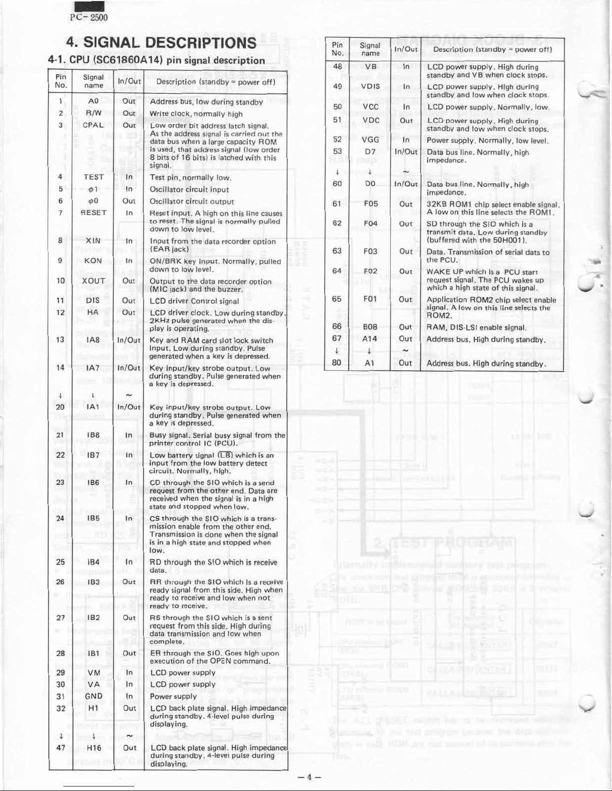
4-1. CPU
Pin
No. name
1
2
3
4
5
6
7
8
9 KON
1
0
11
1
2 HA
1
3
1
4 IA7
.j. .j.
20
21
22 IB7
23 IB6
24
25
26 IB3
2
7 IB2 Out RS throu
28
29
30
31 GND
32
.j.
47 H16 Out
(SC61860A14) p
S
igna
l
In/Ou
t
A
O
O
ut
R/W
CPAL
TEST
(/)
(/J
RESET
XLN In
XOUT
DIS
IA8
1
O
Ou
t
Ou
t
In
In
Out
In
In
O
ut
O
ut
O
ut
In/Out Ke
In/Out
-
IA1
I
IB5
IB4
VM
VA
B8
IB1
H1
.j.
In/Out
In
In
In
In
In
Ou
t
Out
In
I
n
I
n
Out
-
in
signal
D
escription
Add
ress bus, low during
W
rite
L
ow
order bit
As t
he
data
bus when a large capacity ROM
is
used,
8 bits
signal.
Test pin,
Oscil
lator circuit input
Oscillator ci
Reset input. A
to
reset. Th
down to
I
nput from
(
EAR
ON/B
RK key in
down
Output to the data
(MIC jack) and
LCD
dri
LCD driver clock. Low during
2KHz
play is oper
y and RAM
input. Low during
generated when a key
Key
input/
during
a key is de
Key
input/key
during
a key is depressed
Busy signal. Serial
printer control IC
Low battery
i
nput
circuit. Normally, high.
CD through
request
received when th
s
tate and stopped when low.
CS
through th
mission enable from the other end.
Transmission
is
in a hi
low
.
RD through th
data.
RR through the SIO which is a receive
ready signal fr
r
eady
ready to receive.
reque
st from th
data tran
compl
ER
through the SIO. Go
exe
cution of the OPEN com
LCD pow
LCD power supply
Power
LCD
back p
during
displaying
LCD back plate si
during
displaying
(standby= power off)
clock, normally high
address la
address signal is
that
address
of 16 bits) is
normally
rcuit outp
high on this line causes
e signal
low level.
the data rec
jac
k)
to
low level.
ver Control
pul
se gen
erated when the dis-
ating
card s
key
strobe output. Low
standby.
pressed
strobe output.
standby. Pulse generated when
signal
from the low battery
the
from the
e SIO which is a trans
is done when the sig
gh
state and
e SIO which is receive
om this sid
to rece
i\1¬
gh th
e SIO whi
is
smission and low
ete
.
er
supply
supply
lat
e signal.
standby. 4-level pulse during
.
standby. 4-l
.
description
standby
tch signal.
carried
out th
signal (low
latched with
low
.
ut
is
normally pulled
put. Normally, pulled
recorder option
the
buzzer
signal
.
lot lock swit
standby.
is de
Pulse generated whe
.
.
busy signal from the
(PCU).
([B)
SIO
which
other end. Data
e signal is
stopped wheri
and low when not
sid
e. High durin
gnal. High impedance
evel pulse during
order
thi
s
order
option
.
stand
ch
Pul
se
pressed
.
Low
which
is
an
detect
is a send
are
in a hig
h
nal
e. High when
ch
is
a sent
g
whe
n
es
high upon
mand
.
High impedance
e
by.
n
-
-4-
Pin
Signal
N
o.
name
4
8 VB
49
VDIS
50
VCC
51
voe
52
VGG
53
60
61
62
6
6
65
66
67 A14
.j.
80
0
.j.
3
4
.j.
DO
F05
F04
F03
F0
F01
B08
.j.
A1
In/Ou
t
Descript
ion (stan
In
LCD
power supply. High dur
s
tandby and VB when clo
In
LCD
pow
sta
ndb
y and low when clock stops.
In
L
CD pow
er supply.
Out
LCD pow
standby and low
In
Power supply. Normally, low lev
7
In/Out
Data bus
impedance
dby =power off)
ck stop
er supply. High duri
Nor
mally, low
er supply. High
lin
e. Normally, high
.
duri
when clock
ing
ng
ng
stops.
s.
.
el.
-
In/Ou
t
Data bus line. Norma
impedance
Ou
t
32KB ROM1
A low on this
O
ut
SD
transmit data. Low during standby
(buffered with the 50H001
Out
Data. Trans
t
he PCU
2
Out
WAKE UP which
requ
which a high state of th
Out
Application ROM2 chip select enable
signal. A low on this line selects the
ROM2.
but
RAM,
Out
Addre
.
through the S
mission of serial data to
.
est signal.
DIS-LSI enable signal
ss
bus. High dur
-
Out
Address bus. High during
l ly, high
chip s
elect enable
line s
elects
IO which
is
a PCU start
The PCU wak
is signal
ing
signal.
the ROM1
is
a
).
es up
.
.
standby.
standby
.
.
Page 5
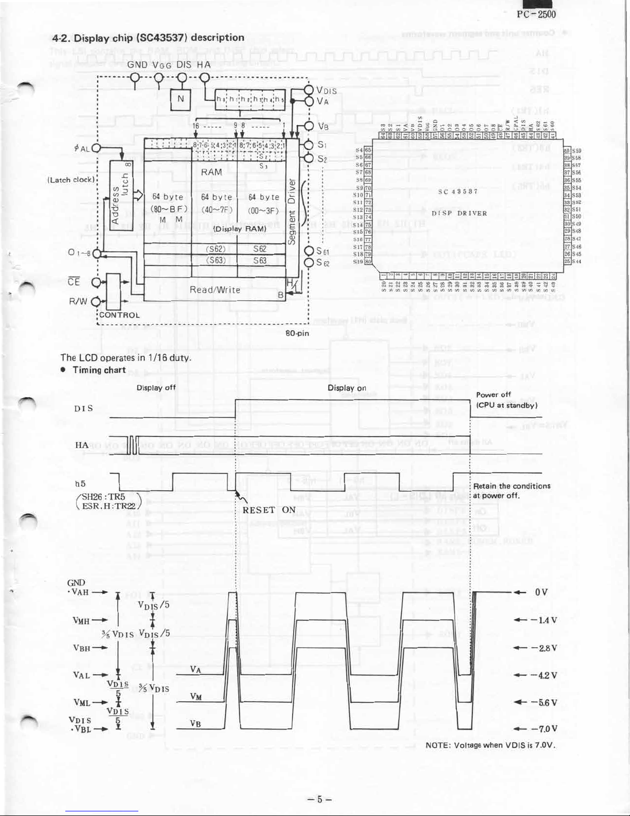
4-2. Display chip (SC43537) description
G
ND
V
GG
DIS HA
-
- - ---
-)}
- ·
¢AL
(Latch clock)
0
1-8
~~---.
C
E
R/W
'
,
:CON
(/)
C/)
-
Q)
~
"O
"O
<(
TROL
s:
u
:J
co
<j>- ~
':.
::'
64
(
80-B F)
M M
byte
-
64 byt
(40-?F
(
S62
(
S63
R
ead/Writ
ho; h 1:h 2:h
' '
e
)
(Display RAM)
)
)
e
J:h ,:h I
'
64
byt
(
00-3F)
S62
S63
PC-2500
-
V
ors
V
A
V
B
S
1
S2
Q:;
>
~
e
0
c
)I
Q)
E
CJ)
Q)
Cf)
O
ss1
QSs2
.
gN~~~~~~~~~~~~~~~~~~~
B
mmmmmmmmmmmm
SC
43537
DISP DRI
mwmmwmmm~mmm
VER
;~
~
The LCD
• Timing
GND
·VAH-
operates in 1 /
DIS
h5
SH26 :TR5
(
ESR.H:T
chart
l~' --~
R22
16 duty.
Display
)
f
VMH
-
I
Vsu..:I""
*
v"
f
80-pin
off
LC
RESET
.......
,.....;
/
5
:
r-«
ON
Display on
Power
off
(CPU at standby)
Retain the
at
power off
conditions
.
-
- -l.4V
-
ov
-2.8V
V
VAL
-
t
VDI s %
5
VML
-
T
VDI
·V
VDIS
S
-
BL- I.
5-
I
Vn1
l
s
A
VM
VB
-5-
~
.__
-
NOTE: Voltage when
- -4.2V
..._ -5.
- -7.0V
VDIS
is 7 .OV.
6V
Page 6
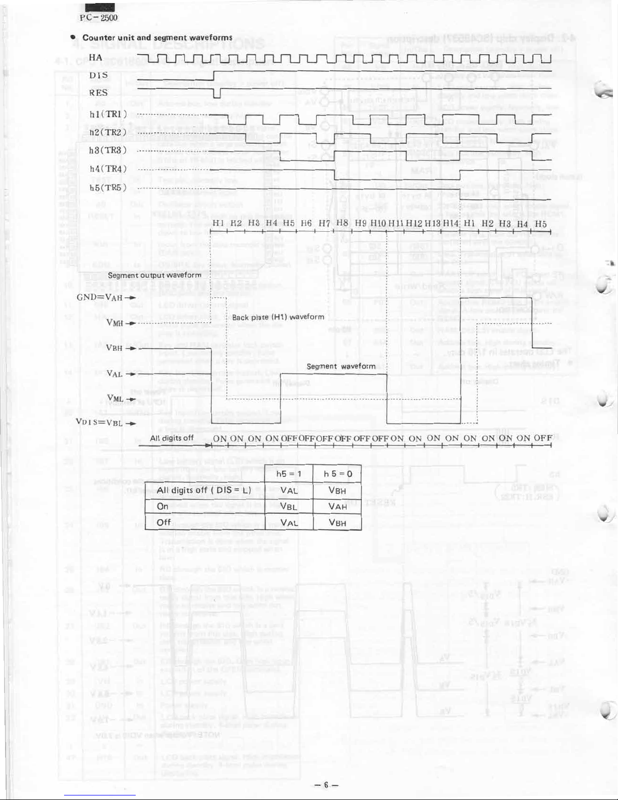
PC-2500
-
• Cou
HA
DI
RES
hl (TRl
nter unit
S
)
and
segment
waveforms
h2 (TR2
h3(TR3)
h4(TR4
h5(TR5)
GND=VAH
VMH
VBH -- ------~
V
DJ
S=VBL --
)
)
Segment output waveform
-
-- --
----
------------------
All digits of
f
Hl
-
ON ON ON
H2 H3 H4 H5 H6 H7 HS H9 H10
B
ack plate (H1) waveform
Seg
ment waveform
ONOFFOFFOF!FdFFOFFOFFON. ON ON ON ON ON ON ON OF
Hl1H12H13Hl4
H1 H2 H3 H4 H5
F
A
ll digits
O
n
O
ff
off ( DIS=
L)
h5 =
1
h5=0
VAL VBH
VBL VAH
VAL
VBH
-6-
Page 7
PC-2500
-
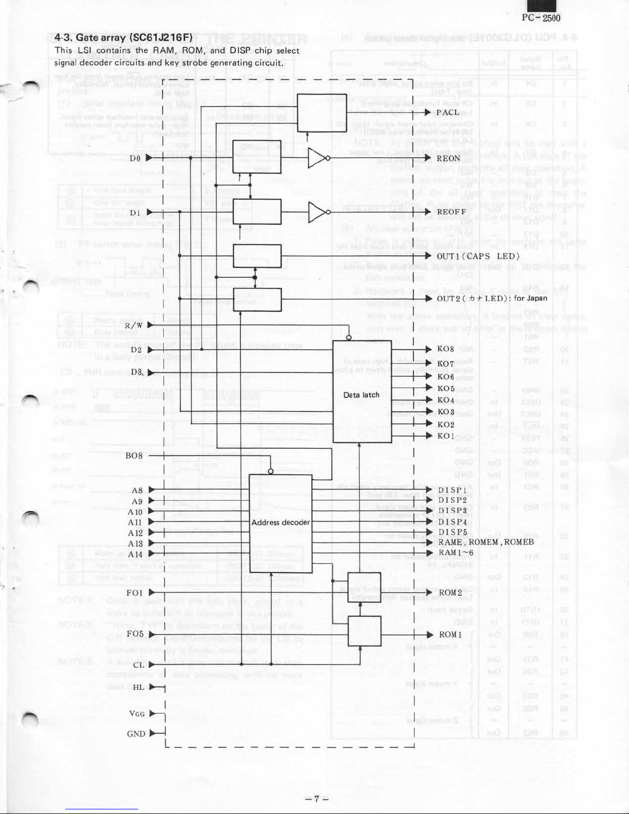
4-3. Gate array (SC61J216F)
This
LSI
signal
decoder circuits
contains the
RAM,
ROM, and DI
and key strobe generating
SP
chip select
circuit
.
------1
I
I
I
I
...
O
l
....
~
....
I
I
I
I
I
I
I
I
I
I
r
!
I
D
D
•
I
i
--{)
I
I
I
...
R/W
....
I
...
r
..
....
I
I
D2
D3,
I
I
Data latch
I
I
I
CL
...
...
...
r
...
....
...
....
~
....
...
r
...
...
...
....
...
r
...
....
I
I
I
I
I
I
I
I
I
I
Address de
I
I
code
---
r
-
,___
I
I
I
-
I
BOS
AS
A9
AlO
All
A12
A13
A14
}
.
FOl
F05
...
P
ACL
r-
I
I
I
...
,
REON
I
I
I
...
I
,
REOFF
I
I
I
...
O
UTl (CAPS LED
-
I
I
...
I
OUT2
(
...
7J
I
I
I
...
K
OS
....
I
...
K07
....
I
K06
I
...
...
K05
I
...
K0
4
.
I
...
K03
r
...
I
.
K
02
...
K
Ol
.
I
I
I
I
...
,
DISPl
...
I
DISP2
.
I
..
DISP
...
...
I
....
..
....
I
...
I
...
3
DISP4
DI
SP5
RAME,ROMEM,ROMEB
RAMl-6
I
I
ROM2
...
I
I
...
I
R
OMl
...
I
I
7
LED)
:
)
for
Japan
HL
~
I
VGG
~
GNDH
L-
----
-
-------
-7-
-
-~
Page 8
PC-2500
-
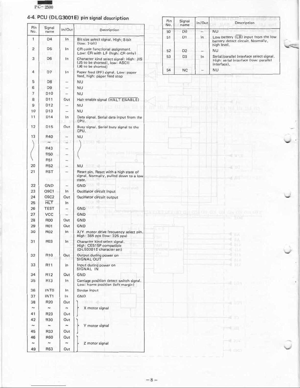
4-4. PCU (DLG3001
P
in
Sign
al
No.
n
1
2
3 D6
4
5
6 D9
7
D
8 Dl
D12
9
10
11
1
13
(
20 R52
2
22 GND
2
24
25 HLT In
2
27
28
29
30 R02 In
31
32 RlO Out
3
34
3
36
37
38 R20
D
D14
2
D15
R40
R43
R50
R51
1
RST
3 OSCl In
OSC2
TEST
6
vcc
ROO
ROl
R0
3
R11 In
R12 Out GND
5 R13
I
NTO
INTl
-
41 R23 Ou
42
R30 Out
- -
45 R33
4
6
R60
-
49
R63
ame
D
4 In
D5
D7
DB
lO
1
13
-
3
-
-
In/Out
In
I
n
I
n
-
-
-
Ou
t
-
-
I
n
Ou
t
-
-
-
-
-
-
-
-
Out Oscillator circuit out
-
-
Out GND
Out
In
In
In
In
Out
-
t
-
Out
Out
-
Out
E)
pin signal description
D
escription
B
it size sel
(low: 7
CR code func
Low:
Character kind select signal: Hi
(J5 to
(J6
P
aper feed (PF) sign
feed, hig
NU
NU
N
U
Halt enable
NU
NU
Da
CPU.
Busy signal. Seri
CPU.
NU
ect
signal. High; 8-bi
-bit)
tional
CR with LF (high: CR onl
be shorted
to be
shorted)
h:
pape
ta
signal. Serial
assignment
),
low: ASCII
al. Low: pape
r feed sto
sign
al (HALT ENABLE)
data input from
al busy signal to the
(
NU
Reset pin.
signa
state
GND
Oscillator
GND
GND
GND
X/Y
High: 365
Character kind
High: CE515P
(DLG3301 E character se
Output during power
SIGNAL OUT
Input
SIGNAL
Carriage
Low: home position
Strobe inp
GND
}
}
}
Reset wi
l.
Normally,
.
circuit input
motor
pps
duri
ng power o
IN
position dete
ut
X motor s
Y
motor
Z
motor
th a high state
pulled down to a low
put
drive fre
quency se
(low: 325
select signal.
compatible
ignal
signal
signal
t)
on
n
ct
switch signal
(left m
p
pps)
t
.
gh: JIS
lect
argin)
y)
P
in
Signal
No.
name
50
51
52
53
r
the
of
pin
.
.
54
D
Dl
D
NC
In/
Out
O
2
D
3
NU
-
Low
I
n
ba
ttery
high leve
N U
-
Serial
I
n
High: serial interface
i
nterface
-
N
U
/parallel interface sel
Descriptio
battery (LB) input
detect circuit. Normally
l.
).
n
(low:
from the low
,
ect
signal.
parallel
-8-
Page 9
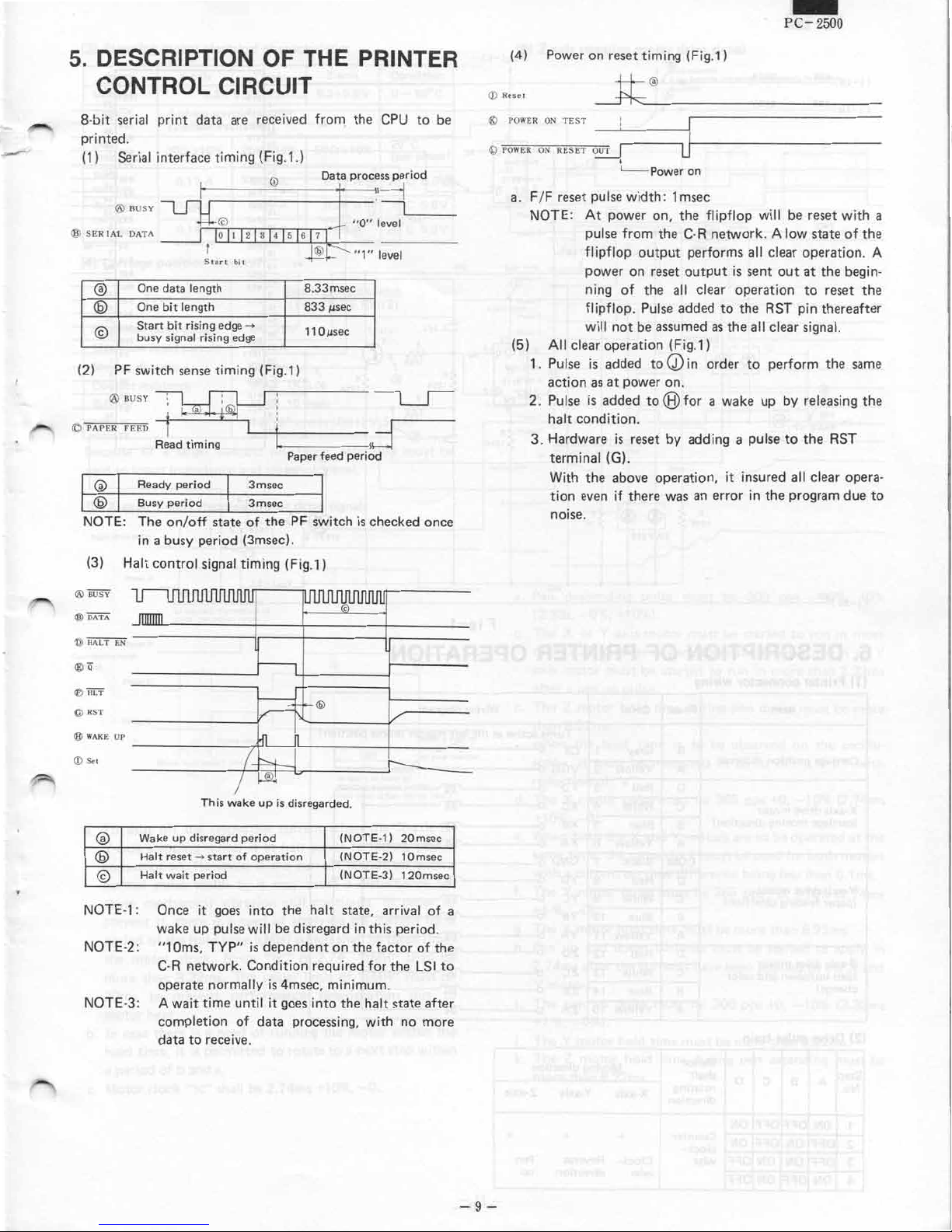
5. DE
SCRIPTION OF THE PRINTER
(4)
Power on
reset ti
ming (Fig.
1)
PC-2500
-
-
CONTROL CIRCUIT
8-bit seri
printed.
(1) Ser
®
•m.c ""' ~
(2) PF switch sense
©PAP
NOTE:
al
ial interface
@BUS
One data le
®
@ One
Start
©
busy sign
@BUSY
ER FEED
Ready period
®
Busy period
The
(3) Halt
print data are
timing (Fig.1.)
Y
~ I__
bit
bit rising ed
Read timing
on/off state of the PF switch
in a bus
control sign
© "O" level
1°1
•
l•l•l•[•[
I
Sta
rt bi t
ngth
length 833 µse
qe
al rising edge
y period
-»
timing (Fig.1)
'-----1----
3msec
3msec
(3msec)
al
timing
received from the
®
O
J
''°':''''td
•i
@
"1" level
8.33msec
c
11 Oµse
c
Paper feed
.
(Fig.1)
perio
is
CPU
to
----i__s-
1
~
d
checked once
be
Q) Rese
t
1!9
POWER ON TEST
IQ
POWER ON RESET
a. F/F
NOTE: At power on, the flipflop
(5) Al I clear
1. Pulse is
2. Pulse is
3. Hardware
_jt
~
L_
reset pulse
action
halt condition.
terminal
With
tion
noise.
width:
pulse from
flipflop output
power
ning of
flipflop. Pulse added
will
not
operation ( F ig.
added
as
at
power on
added
is
(G).
the
abo
even
if
_
Power on
on reset
the
be assumed as
to
to
reset by adding a pulse to
ve
there
®
---
J
f------
1msec
the C-R network. A low
performs all clear
output
all
clear operation to
to the
the all
1)
Q)
in
order to
.
(8)
for a
wake up by releasing
operation, it in
was an error in
-----
will be
is
sent out at the
RST pin thereafter
clear si
perform the same
sured all
the
program
--
reset with
state of the
operation. A
begin
reset
the
gna
l.
the
the
RST
clear opera-
due to
a
-
Th
is
wake up
@ Wake up
@ Halt
Halt
©
NOTE-1: Once it goes
NOTE-2: "
NOTE-3: A wai
disregard pe
reset
-»
start
wait period
wake up pulse will be disregard in
IOms.
TYP"
C-R
network. Condition
operate
completion
data to
normally is
t time
receive
is
disregarded
riod
of
operation
into the halt
is
dependent
4msec,
until it goes
of
data
processing, with no more
.
required
into the halt state after
.
(NOTE-1)
(NOTE-2)
(NOTE-3)
state, arrival of
on
the factor
minimum.
this
period.
for the
20msec
10msec
120msec
of
LSI
a
the
to
-9-
Page 10

(
l-IH)IF03
(
1-IH
(1-1 H
PC-250
0
-
'
I
BB
'
)
PACL
J
®
DAT
BUSY
A
®
®
Ci)
--1
I
__
DAP202
CD
GND(O
)
VGG(-5)
TC
CD
NU
36
INTO
N U
®
1
OOP
G
ND
0.
1
©
1 OOP
GND( 0
1
OOK
D2
32 39
Rl
0
33
Rl 1
23
2
4
P
C U
DLG3001 E
N U
1
9
R52
R53
D
12
L ':
10
Dl
3
5
4
NC
30
R02
3
7
R03
R
l 2 D5
2
1
RS
T
Dl 1
22
G
ND
)
G
N D
R
TEST
VCC
R20
R
R22
R23
R30
R3
R
R
D10
R6
R6
R
R63
RO 1
ROO
l 3
21
32
33
62
D
D9
D3
D4
D
Dl
DO
D7
35
26
27
38
4
0
41
4
2
1
B
0
1
4
9
2 9
2 8
53
6
51
5
0
N
U
(!-3G)PF
6.
DESCRIPTION
(
1) Printer connector wiring
Ite
m
Carriage position d
X-ax
is dr
ive
(carriage mov
Y-axis dri
(pap
Z-axis drive moto
(pen up/down and color
ve
er feeding
motor
ing
direction)
motor
direction)
etector
r
change)
-
I
I
1 OOK
I
L
DA P20
I
_J
2
OF PRINTER
P
hase
C
olor
G
ray
B
Y ellow
A
D Red
White
c
Blue
B
Yellow
A
Black
COM
Red
D
While
c
Blue
B
A
Ye
llow
Red
D
White 13
c
Blue
B
Yellow
A
1
H
Turns active at
1
c
s
VGG o
2
XD
3
4
xc
XB
5
6
XA
7
GND o
YD
8
YC
9
YB
10
11
YA
ZD
12
zc
14
ZB
ZA
15
VGG
F
ig-1
OPERATION
W
iring diagram
the le
0
-
-
-
-
-
-
-
-
-
-
-
-
-
ft
margin (home position)
o~
uu
uu
00
vu
vu
o
o
00
uv
00
uv
I
VGG(-5
1
OOK X 2
©
)
(
2) Drive pulse
Step
A
No
.
1
ON
OFF ON
2
OFF ON
3
ON
4
train
B
D
c
OFF OFF ON
OFF ON
O
FF
O
N
OFF ON
OF
F
Mo
tor
shaft
r o
tating
direction
C
ounter
clock
-
wise
X-axis
-
C
lock
wise
Moving dir
Y-axis
+
Reverse
-
direction
ection
+
Z-axi
Pen
up
s
+
-
10
-
Page 11

(3) Stepping
Item
Voltage
Type
DC
resistance
Peak
c
urren
t
Averag
e
cur
ren
t
per phase
motor electrical
X-axis
5.3 ± 0.5
4-phase stepping
(2-pha
se
excitation)
30.!1±10
0.17 A 0.21
0.24
0.14 A
2
%
A
characteristics
Y-axis
V
mot
5.!1± 10% 50.!1± 10
A
0.29
A
0.16
A
Z-axis
5.3±0.5V
or
0.12
0.26
0.09 A
%
A
A
C
onditio
0 - 50°C
20
°C
(per phase)
20°C
5.3
0°C
5.8
20°C
5.3V
PC-2500
-
(6) Z-axis stepping
n
motor
drive signal
Ipnnt exemcte
A
illustrated.
pen
descends, and
l
ascends a
fter
drawing the figure a
s
j
@
Basic
pulse
z-axismotor
Phase A
Phase B
Phas
e C
P
hase
--~
D
V
V
©
(4) Carriage
Maximum rated voltage
M
aximum rated curren
Moving distanc
Contact
Bounce
Life
Because of a larger
paid to input impedance and thresho
(5) X-a
B
asic dri
Counterclockwise
rotation
a. To shut off the respective
Y-axis stepping motor
con
position detecto
Type
resistance
xis, Y-axis
ve pulse
_
Pha
se
A
__J
Phase
B
Phase
D
-
Motor lock
sumption.
r
Elastic
(Type: KEG 10
DC 12V
t
20mA
e
0.8 mm
M
AX
MAX 1
1K.!1
0 msec
1x10⁵ cycles(DC12V 5mA)
conta
ct
resistance, att
stepping
...L._....L _ _j_ _ _._ _ _._ __
Depending on
locati
on the l
be
applied, the me
pulse i
mpression varies
-+-
--'
state 2.74
t
C
what
ock should
thod
___.
M
otor cl
ms
motor dri
of
.
l
ock
current when the X-a
is
at
halt serves to reduce power
However, if the
current
contact
ention must be
ld level.
ve
signal
s
~
-------
'
I
1_
- - - - - - - - - '-----
,_
.,.___t=M~H
Current is
to apply in
maintain a proper
Halt time: 9.2ms (20ms, ma
is
shut off wi
switch
012)
continued
order to
normal pulse width b, it may cause a disturbance be-
cause mechanical vibration still continues.
prevent it,
there
is a
need of applying the cur
period of the hold time (tMH) which shall be three ti
the
motor
more than
20ms
motor
b. In
case there
hold time,
a
period of
c.
Motor clock
clock. Since "tc"
8.22ms. The upper
to
prevent performance
heat
.
is a need of running
it
is
permitted
band a.
"tc"
shall be 2.
is
2.74, "
tMH" shall be
limit
of "tMH" must be
deterioration due
the
motor
to
rotate to a next step within
74ms
+10%,
-0.
@
._!
~ _
__,,.to stop
tempo.
xis or
In or
der
rent for
within
--
Hold is
used to
apply in order
rotat
x.)
th
a
to
a
mes
to
the
_
ion.
Bas
ic pulse
Phase
A -----'
Phase
B
Phase C -----'
Bas
ic
puls
e
Phase A -
Phase
8
otor ----------
Phase
C
P
hase
0
Up t
on
n
is
position
-----------
------'
Kept stable
as it is pulled
he magnet, not by a pulse
by
X-axis motor
Y-axis m
P
en positi
X-axis positio
Y-ax
a. Pen descending pulse mu
(3.
33s, - 0%, +10%)
.
b. The X or Y axis motor must
than 3.33ms af
ter a pen
axis motor must be st
after a pen
c. The
than 8.
when
scop
r
eduction of "a".
d. T
he X motor pulse must be 365 pps +O, -10% (2.74ms
+10%, -0)
up pulse.
Z motor hold time
22ms
.
the hold time
e, it must be
measured in
.
e. When both the X and Y motors
s
ame
time, the same clock must be used for both motors
with a current
f. The Y
+1-%, -0)
on time difference bei
motor pul
se must be 365 pps +O,
.
g. The X motor hold time
h. Pen up and down curre
2.74ms after the
Y
motors
.
i.
The pen up pulse must be 300 pps
+1-%, -0%
j.
The Y motor
currents
).
hold time must be more than 8.
k. The Z motor hold time
more than 8.22ms.
+-
-----------
CD
Down
st be 300 pps
be
started to run
down p
ulse. Also, the X or Y
arted to
is
run in more than
during
pen down must be more
to be observed on the oscillo-
-10%, +0%
terms of "c +
are to
be
operated
ng less than 0.1 m
-10% (2.74ms
must be more than 8.22ms.
nts must be started to apply
have been
applied
to
the X and
+O, -10% (3.
22ms.
during pen ascending must be
in
a'"
more
3.3
at
33ms
-
3ms
with
the
s.
in
-11 -
Page 12

7.
PARTS
&
SIGNALS POSITION DIAGRAM KEY P.W.B. (KEY TOP SIDE)
Japan Only
- 12-
Page 13

~p
SIDE)
PC-2500
-
-13 -
Page 14

8.
PC-2500
-
KEY
P.S. P.W.B. (LSI
SIDE
)
Qi
P.S Pll
SLOT PW
:1(5:
JAPAN
EX.
-
14
-
)5
:1(4
:
JAPAN Short
EX. Open
]6
Open
Short
Page 15

Nl
N9
NS
N3
P.S PWB
i9:i
SLOT PWB
Key PWB
Chip Tr,
Di
•
C2412--
2SC2412S
•A 1037-2SA1037S
•
P202--
DAP202
•
N202--
DAN202
~
(El
w
(!]
A
A
Chip Capacitor
•
100PF--A2
•
1000PF--
•
0.01
µF--
•
0.1 µF---
• 0.
033 µf--
• 0.
022 µF--
A3
A4
AS
N4
J4
:l'.4:
JAPAN Sho
EX. Open Shor
J
5
rt Open
1
6
t
- 15-
Page 16

9.
SLOT & P.S. P.W.B
CN
,- - - - - - - - - - - - - - - - - - - - - - - - - - - - - - - - i
6
,~
,
(0
'
'
,
I I
,_ - - - - - - - - - - - - - - - - - - - - - - - - - - - - - - - _ J
~~~~~MN
~w
> uo<OCCOCCOOo<<<<<<<<<<<<<<<<<<OC>~
ocOC
....
u.1
0(1)
Z::>
~
1-----+-~~~~~~~~~~~
I
I
I
c
i
I
z 0 0
~
oc oc
I
·-
----
c:)
N'
z
::!:
~
o
Print
oc
er<;
to
8
>
CD
~
w
::!:
<
oc
-
o~~~~~~~~~~r--.~&n•MN-o~~
::!:
OC
w
r--.
in M -
0 0 0 0
CD
...
0 0 0
~
....
oc
< < < < < < <
0
...
"'0
0
"'
z
u~
< <
Cl)
o
~
~
~
"'
0
x x x
f
r_o_m~k-e-y~P-W-B~--.
"'""'""~~~
CIC)
CD
....
< < < < <
<
CD
o
<
x
~
"'
0
z
oc
0
0
> >
0
z
~
o
~
CD
>
o~
'
'
q:
,
,
~
0
CD
o
N N N
<
<
>
N
BUZZER
1
BLACK
I
-16-
Page 17

P
C-25
00
-
3
~
N'
N
(..)
o
F
50V
to Key
PWB
......
....
0
;::;
EID
(..)
I
o
a:
-3 -~2
_'
I
ADAPT
REM
I
,Q
.••c
~EAR
CONTRAS
OR
T
1
<.-----
,--G--,
I
<p
I
§:
I
en
I
1-
I
w
I ~ I
I
a:
I I
,_ - -
,..
-
~
0
"'
"'
o
I
<t
I
I
I
I
I
J
Jo
\
I I
11
\
\
\
~
~---)o-
FG
RD SD
CS
RS
SG (NC)
(NC)
CD
RR
Vee
vc(NC) I
(NC)
ER
FG
1 I
-
--
'
I
I
I
I
I
I
I
I
:
o
l
I
CN4
SIO
-
17
-
Page 18

PC-2500
-
10.
LCD P.W.B.
-18-
Page 19

CN9
-19 -
Page 20

11. CIRCUIT DIAGRAM
o [ s
p
1
SC+3537
v
,
LCD
LF-7136E
DISP
SC 43537
56
DlSP
1~110
5211 .... HO
3
S
m-1so
'
L
D!sp
SC+3537
4-
S1-3o
S
11i-1t
o
2
.$31-60
S1M-210
SC+3537
....
C
HA~~E.
(EA·1SO)
t_,..1
~TC
SOHOOl
l
j
r'•
ar;.-.
s,1r; •
....
v,..
..,.T
ROM
SC 613
25 6 F
PS
4
3
!;Ai[)
¥i
0TTAMTLctif-HH
x
a
fil
CPU
SC 618
60A14
1
RESET
o.on/'
rop
•~
r
I
ROM
2
SC 6132
ce
R
CNS
5 b FPS 44
(
Japan)
H
J
: - - ~D
apan Onl}
:,,)- -:
NO
S~K
~llTf ~;, ~S)
o
\;<!<
;
~t-~
_N_;_C_d
S
o
l;'
10DI 10£>1
"'"'
-!4-
---'--
~~'-
'"
_.._
__._'_'°_'_'_+-;-:~
2'20K. I ~~
-20
-+-:-o',_
22.
-
.ll.fw
'l'
'M-
-....__<l'·~')'
'-""--+----
----------
CH12
'-"
_.~
.._
1_·'_'
Ok
C
t4f'l.
_;_''_'
-
- -- _J
I
_
I
__.._._'
Page 21

PC- 25
00
-
GATE ARRAY
SC 61J 21
6F
EA
R
M
IC
RE
M
l'AC
L
pc
u
D
LG
3001
E
Jap
an
Onl
y
C.APS)
"'
l
.H
Uk
I
'
Ct4U
-- --
I
!
_J
'
"
C
':l.02
1-R
-
21
-
Page 22

PC-2500
-
12. PARTS GUIDE
,-----
I
I
,
I
-------
50
----
~
I
I
l
62
I ~ ..... ~~
I "'.........
L
,---
------
I
(
Japan)
I
I I
I
I
I
I :-~
1
I
71 lW
I
1
1
66
J
i
m
PEN 1
D~F P;N
DEF
~---
- -
....
-::
----;
---;-- -~- - - -
E~
J
o
ITJ
EJ
,
l
Q,DDEJEJEJDD
'"'"l
WEJIJ_QQ_E]QJil_OJ·"''"[DDDEJ
70 69
-
D
:
I
ITJ
~
EJ
--
- MC
- MODE
m w m
EJ
....
...- :;=_::_~~~
~u~~-"A...a..h...l...
------------
oN/BRK o!'l1B11K 0N1
ON/BRK ON/
BRK ON/BRK ON/BRK ON/BRK
c
L11
OLDRE
-~
~ - - -
:-
"7'..'.":
~ ~ :~ EJ
--- _(
[l[:j
0ftJ--~--
-
)
=====-:.-_
--~-
------~:=======
E3 Q EJ
EJ
EJ
EJ EJ
w
llJ!:D D D
Q~
j
'
""'
6
8
67 66
A..l)•.
-
:
CW/BRK
=--:-i-~=-----~~
-1
0N1e11K
f~l
EJ
!
:
:
65
,
e11K
C:]
[C]~E::~:~f~! I
qJJ;~~Lru
,,
j
DDDEJ
[
l
eo:J
_
O
[J
EJ
~
--------------------------~
,----------
(Export)
~--
m
r
EN ,
D~F P;N . :
DEF
~--
0l
71
,_l
66
I
:
L----------------
-
~n::J~Jr:r0E:J~c
J
EJ
DD DD
~
DDDDEJDDDDD
'"":~
DE]D_D_D_DEJO_OF:.
"'
70 68
I
--___J
-
--
-
c
L11
- MCOLDRE
- MO
DE
---------
0N1
e11K 0N1BRK 0N1e11K
~:;::: ~:;::: ~:;
63
/ ON/BRK ON/
~
t~
[jf[J--~--
.
!
~
r
CJt'.ltJ=c:rn!t~
EJ D EJ
BRK ON/
E=:J
D
<ITT
"
67
rr::::::J
c:J
i
'"
66
---
-
---,
0N1
ON/
BRK ~:;:::
BRK ON/BRK
:
CN/BRK
n
:::sfti
0
E'.:'.::5~
e11K
:::
BRK ON/
E:::]
f
jtftfo;EJ!
i
DDDD
1
0
o o
EJ: I
L
C':J .O_
O
[l
---
-
l
6
5
i
-~
I
I
I
I
I
:
l
I
I
I
I
I
l
I
I
J
I
i
J
l
J
f
l
l
I
1
1
45
i
4 7
:
~
//
I
,/-
_/,/ ~A
~
60
~:.
,,!,,--.,
'~'
(
I
I
I
q5
.
-,
<,
<,
<,
<,
51
-
22
-
Page 23

5
7
.
Note ·
. e slot
Th
the p S
-23-
PWB
. . WB.
p unit will
.
in supply in a .
be
.
p
a i r
wit
h
Page 24

13. PARTS LIST
[I]
tI
.mRB£(Mechanism parts)
NO.
PARTS
CCOVA1
1
CC
OVA1414CC01
2
HBDGD
NSFTZ1078CCZZ
3
4
PTPEH1195CCZZ
PF i LWl 5 2
5
PT
PEH
6
HDECA2176CCZZ AF
7
HDECA2176CC01
GC
ABB
8
GCABB2829CC03
XUPSD
9
XUPSD26Pl0000 AA DA
1
0
11
PZE
12 QCNW-1319CCZZ
PGUMM1568CC01
13
14
MSL i P
15 QCNTM1042CCZ
MSLiP1034CCOl
16
DUNTK8467CCZ
1
7
DUNTK8473CCZZ
P
GiDW1043CC
1
8
19 PGiDW1045CCZ
PGiDW1044CCZZ
20
21 PFiLV1003ECZZ
22 PGUMS
23 PGUMS1583CCZZ
DUNTK84
24
LHLDZ1223CCZ
25
XUPSD20P
26
QCNW-1317CCZZ AB DC N
27
28 XUPSD20P05000
DUNT-
29
PT
PEH
30
PS
LDP
31
PZETL
32
PTPE
33
34 DUNTK8465
CODE
414CC02
137
6CCZZ
8CC
1280CC
2829CC02
26P05000
TL 12 2 OCCZZ
l034CCZZ
1567CCZ
66CCZZ
8254CCZZ
1039CCZ
1487CCZZ
1552CCZZ
Hl 280CCZZ AA DA
ZZ
ZZ
Z
Z
ZZ
Z
Z
Z
08000 AA DA
Z
CCZZ
PRICE RANK
Ex
AQ
AG
AC
AG DU
AA DA
AU F K
AA DA
AF DP
AP
AP
AA DA
AA DA
AK DZ
AS F
AB
AA DA
AA DA
BX TR N
BX TR
AA DA
AB
AA DA
A
F
A
C
AA DA
BT
AB
AA DA
BC
AA
AE DL
AC
BP
Ja
ET
DR
DC
DM
EN
E
N
C N
DB
DB
D
Q
DE
NP
DB
GQ
DA
DD
MC
NEW
MARK
PART
RANK
N D
N D
N
N
N
N
N
N
N D Too
N
N
N
N
N
N
N
N
N
N
N
N
N
N
N
N
N
Pape
Paper cov
c
M
odel badg
c
Roll shaft
Ta
c
c
A
crvt filter
Tape
c
Dec.
c
D Dec. oanel (Ex
D
Top cabinet
Screw (2.6X
c
Screw (2.6X10)
c
c
Insulator sh
FPC (40pin)
c
K
ev ru
c
c
Slide switch knob
c
Slide swi
c
Slide
E Key PWB
E Key PWB unit (Ex
Guide pin
c
c
Guide
Guide oin (Ent
c
Polaized filter
c
c
Rub
c
Rubber
E
L
CD PWB uni
Rubber
c
S
crew (2X
c
F
PC (5oin)
c
Screw (2X5)
c
E
L
CD
L
CD
c
c
Shield
Insulator
c
Tape
c
E
Power suno
r cov
er unit (Ja
er unit (Ex
pe
oanel
cabinet (J
bber
tch
switch knob
pin (Space·bar)
ber con
connector
connector
uni
t
fixing tape
plate
e
(Japan)
oort)
apan)
(Exoort
5)
eet
terminal
unit (Japan)
port
(Shift
)
er)
nector
t
8)
sheet
lv PWB un
pan
)
port
)
)
holder
it
DESCRIPTION
,-..!!_-r~-t.J
)
~-r{°-1Jr{-.::i.....
.f:T'Jv/<
O-)v/
7-7'
7
T~:J
:f":J.1{*JV
'7
CJ.I.~
t'J.
l:A.
~-FPC3'7
FPC
~
7..71
7.. 71
7..
~- ~,,/
~- ~/{
tf1 rt:"
1f1 rt'/
1.t1 rt'/ i/J-
r-; /
LCD ~,,/
FPC
LCD
LCD
-t'•/
7"/Y/
.1
<- .i..::..
·;
-f
-1"
7
1
J
:7
Jv71 Jv
1
)
3
'7
j
/7-7'
/..f?;f-JV
.I. ~
-\"
I:
1· ·;
-\"
l:;f.·;;
-::f
J.,,
J-'7,1·1+
r
·
7.. 1 ., + 01 /J
71 ~·7,1
.x.:z: .,
',/ ;i;::_ '/
/
;7..«
01
7 7
;f.;7J-
a.
s: .,
"
717-7'
.I.//-
1
;7 J-
-
/
01'J.,, OJ;f,
01'J.,,01
01'J.,,01;f.;7J
\:7..
\:7..
~-1t--V ,,,
1)3');>1/7-/
~,
..::..
";
f
J-
f
f
?17-/-
·:;
+
-;7..
1v
J -
.i:::- ·:;
;j;:J
f
I-
,y
.i- ·
"/?
'/?:
I
·
f
3
·
;;
r
l-
f
:
:7 I·
f
'7:7
1
f
37 QCNCW1
38
39
4
0
41 MSPRC1299
42 XUBSD26Pl2000
43
44
45
46 LHLDW
47
48
4
9
50
51
52
53
54
55
56
57 GFTAB1313CCZZ
58 XUBSD26P
59
60
61
62
63
64 JK
65
66
67
68
69
70
71
72
73
1-1
327CC03
QCNCW1376CC0
J
KNBZ196
DUNT-
QLUGE1004CCZZ AA
QC
NW-1318
QCNCW1373CC01
1201CCZZ
Ki-OB1018CC
GLEGP1009CCZZ
LANGT.13
GCABA2828CC02
GCABA
PTPEH1213CCZZ
RALMB1030CCZZ
UBATN2135CCZZ
PCUSS1113CCZZ
LANGK1573CCZZ AC DE
PTPEH1222CCZZ
GFTAA1287CC05
TLABZ2189CC
T
LABH
2187CC
TL
ABH21
JK
NBZ1952C
NBZ
1955CC01
JK
NBZ1949CC0
JK
NBZ1950CC0
JKNBZ1950CC
JK
NBZ
1951CC01
JKNBZ
1953CC
JKNBZ
1954CC0
JKNBZ1948C
J
KNBZ1948CC02
LANG
T1582CCZZ AB
QCNCW1377C
QOICWl
1
2CC
ZZ
8323CCZ
282
Z
CCZZ
CCZZ
ZZ
4 6CCZZ
8CC01 AP EN
06000
ZZ
ZZ
88C
CZZ
C01
1
3
02
01
1
C01
C40 AP EN
382C
C30
DC
A
C
AC
DC
AA DA
AN
EH
AA DA
AA DA
DA
AL EB
AL EC
DA
AA
BY
RR
AA DA
AA DA
AP
E
N
AB DB
AD DF
AZ
GG
AA
DA
AA DA
AB
DB
AA D
A
AB DC
AB DB
AC
DD
AC DD
AB
DB
AB DB
DB
AB
AB
DB
AB
DB
AB DB
DB
AB
DB
AB
DB
AW F R
D
AL E
B N
B
B
Connector (3p
B
N
N
N
N
N
N
N
N
N
N D Connector cover
N
N
N
N
N
N
N
N
N
N
N
N
N
N
N
Connector
c
RAM
E
Slider
Soring
c
Screw (2.6x12
c
T
c
FPC (30pinl
c
Connector
c
Wire
c
E Printer (
c
R
Print
c
D Bottom
D Bottom cabinet (Export
Tape
c
B
Buzzer
A
Batte
c
Batte
Batte
c
Tape for dee
c
D
Batte
S
c
Caution label (Ex
c
c
Ins
Instruct
c
K
c
K
c
K
c
c
Kev top (Shift
K
c
K
c
K
c
Kev
c
Kev
c
K
c
Angle for S 10' connector
c
c
Comector (40pin)
Comector l30pin)
c
(2pin
card knob
unit
erminal
ubber
crew (2.6X6)
truction
ev
ev
ev
ey top (Enter
ev
ev
ey top (A
)
(l
5oin
holder
DPG29)
foot
er fi
tting
cabinet (Japan
ry
ry
cushion
ry
presser angl
ry cover
label A (Export)
ion label
too (H
alf
top (ON/
BR K ke
top
(I
?Keys)
top (Sp
ace·
too
11rt
too
(Caos kev
top (Alphabet kev)(Japanl
lphabet
in
with wire)
with wire
with wir
angle
)
)
e
pane
l
oort
)
B (Exoort)
kev)
y)
kevl
key)
bar
key
key)(Japan)
)
key)(Export)
01;f.
;7J-
'1;/·:7J
)
es)
)
-
24
-
-
RAM
;/J
- r 3
7..717'-.i:::-·yf
;z7'i)/;7
"
\:7..
7;7"J//
FP
C
01;(.
;7J
-
'71-1'
;J;1v7'
7 /
/J-
'1 ~-\" c ;f.
~
-1"
1:'1··
/;t
/J1
-
T
iJ
-
1
)
7
-
, 7
'J-
;t-tt
01
''*
Jv3 '7
1J
;z
....ZJ'v
7-.::;
f
:;7°
'/ 7°
.,
;
'/
7'
7'
f
y
-;f'
-v
7'
;
7'
/
7'
10
:J
;;f.
7 7
-
-
I-')
:;
3
-
'7
-;f'l) /J-
::JJ.,,
7'1J
')
'/
01
"'
7'-tf
.< "!
,, ·:;
,,.
T
7>+
c
'1;/·:7J-7J
+1717
-t'Y J 1
-t·/J1 7..-.:;v
~-
~-I-
~-I-
~-I-
~-I- !
~-
~-I-
~- f .,
~- f .,
~-I-
s
:J;(,?'.)1
:::i
;;f.?'.)1
'7
J
7·
"l
'T7
/;7
'v
I-
I-
01717-7'
:7 ·:;
/
.r,
7
/
7-
/
v A
B
- 3 ') 7 /
3
;t1v
"J'v
/
[
7·
)!I
Page 25

PC-2500
-
[l]
~5~£f&..:J...::. ·:;
PARTS CO
NO.
LANGT1582CCZZ AB DB
1
QCNCM1338
2
QCNCM1338CCOC
:;
f
3
QCNCW1368CC1E AM
4
QCNCW1373CC01
5
QCNCW1377CC40
6
7
QCNCW1382CC30
QC
NTM1051CCZZ AB DB
8
QC
NTF1065CCZZ
9
QJAKC1003CCZZ
10
QJAKC10
11
QJAKC1016CCZZ AC
12
VCTYPU1NX104
13
14
RC-CZ1077CCZZ AC
RC-EZ105CCC1H AB DC
15
RC-EZ227BCC1A
16
RC-EZ227DCC1C AC DC N
17
RfiLN1008CCZZ
1
8
R
RLYZ2400QCZZ
19
RVR-MB512QCZZ AD OF
20
RVR-Z2400QC
21
VCTYPU1EX103
22
VCTYPU1EX472
23
V
HDD
24
25 VHD1
26
27
28
29
30
31
32
33
3
35
36
37
38
39
40
41
42
43
44
45
46 VRD-ST2H
47
48
49
5
901
S1588L2-l AB DB B
SS98/
VHDlODl////-1 AD DD
VHDl 1DQ03//
V
HEHZ2BLL//
V
HEHZ4
VHiLB1247//-l
VHiTC4013BP-1
VRD-ST2EY102J
VRD-ST2EY103J
VRD-ST2EY104J
4
VRD-ST2EY223J
VRD-ST2E
VRD-ST2EY225J
VRD-ST2EY334J
VRD-ST2EY393J AA DA
V
RD-ST2E
VRD-ST2EY474J AA DA
V
RD-ST2E
VRD-ST2EY681
VRD-ST2EY682J AA DB
V
RD-ST2H
VS2SA937-
VS2SC2021
VS2SD1227MR-1
VS2SJ43-P/Q-
0
.:l.-·:;
DUNT
K8465CCZZ
DE
CCOB
13CCZZ AC DD
ZZ
M
M
//
-1
-l AE DH
-1
ALL//-l
Y224
J
Y473
J
Y563J AA DA
J
Y220J
Y270J AB DB
//-l AB
-R
1- (Uni
t)
M
SC
C
t-
(Power su
PRICE
RANK
Ex Ja
AA DA
AA DA
E
F
AL EC
AP EN
AL EB
AV F L
AD
DH
D
H
AB DB
DE
A
C D
C
A
H D
X
A
P
E
N
AF ON
AB DB
AA DB
AD DH
A
C DD
AD DH
A
M
E E
AK EC
AA DB
A
A
D
A
AA D
A
AA DA
AA
D
A
AA DA
AA DA
AA DA
AA DA
AB DB
DB
AF
D
Q
OF
AD
A E DH
BP MC
pply PWB unit)
NEW
PART
MARK
RANK
N
N
N
N
N
N
Angle for
c
B
Connector (Zpin)
B
Connector (3pin
Connector
c
Connector
c
c
Connector (40oinl
Connector (30pin
c
c
Reset terminal
Connector (35p
c
B Jack for
B Ja
ck for MIC
c
Jack socket (for Remote)
c
Capacitor
Capacitor
c
Caoacitor
c
Capacitor
c
Capacitor
c
F
ilter (ESD-H-14Bl
c
Relay
B
B V
ariable
B
V
ariable
Cap
acitor (25WV 0.01 uF
c
Capacitor
c
D
iode (OS! 588L2l
B Diode
B Diode
B Diode
B Ze
B
B
B
c
c
c
c
c
c
c
c
c
c
c
c
c
c
c
B Transistor
B
B Transistor
B Transistor (2SJ43-P/0-C
E Power supply PWB unit
(1 SS98)
(1OD1
(11 DQ
ner diode (HZ2BLL
Zener
diode <HZ4A
IC (LB
1247
IC (TC4
Resistor (l/4W
Resistor (l/4W lOK
R
esistor (l/4W
R
esistor
Resi
stor 0/
Resistor (l/
R
esistor
Resistor (1I4W 39Kfl ± 5
R
esistor (1/4W 47Kfl ±5%) T1
R
esistor (1/
R
esistor (l/
R
esistor 0/
R
esistor (1/
R
esistor (1/2W
R
esistor (1/
Transistor
DESCRIPT
Sl 0 co
nnector
l
(l Soi
n)
(l
5pin wi
th wire)
)
in)
AC adaptor AC
(12
WV
0.lOuF)
(16WV 1 OOOOpF)
(50
WV 1 uF)
(lOWV
220uf)
(16
WV
220ufl
resisto
r
resistor (20Knl
(25
WV 4700PFl
l
03)
)
013BP-ll
(1/
4W 22K
4W
4W 2.2M
(l/
4W 330Kfl ±5%)
4W 470KO ±5%)
4W 56K
4W 680.fl
4W
2W
(2SA937)
(2SC2021-RS)
(2SD1227MR)
)
)
LL)
lKO
±5%)
fl ±5%)
ioox
n
±5%)
fl ±5%)
220Kfl ±5%)
fl ±5%)
%)
fl ±5%) T 1 :J
±5%)
6.8KO ±5
220 ±5
27.fl
±5%)
%)
%)
l
I
ON
S!O:J:f,·:713'7
:J;f:.:71-
:J;f,J1-
:J:f,:71-
:J:f:.:71-
:J
:f
:71-
:J;f :71-
IJ k·:; f 7
:J:f,:71-
?
'; -\' ':!
:J/f/-tj"
:J/f/-tj"-
:J/T"/-tj"-
:J/f/-tj"
:J/T"/-tj"-
7
1)
;r,·
;r,
:J/T'
:J
1"1:t-l'
1"1:t-l'
1"1:t-l'
1"1:t-l'
"/
'
/:r.t'-7'"1:t-l'
IC
IC
T
71 :Jr;
71
71 :Jr;
T1
71 :Jr;
71 :Jr;
T1
71
T1
T
71 :Jr;
71 :Jr;
f/7'/
;_,;_,
71"
7"1
1:7o;t/
:7
'/
'T
-
-
11v?-
].;
-
IJ
'/ L
· IJ '/ i:
°/-tj"
-
/7'/-tj"-
.r.
f'-1"
1
1
:J
'7
:Jr;
:J
'7
:J
'7
:J
'7
:Jr;
'7
:J
'/
1
:J
'/
l-
7;,s;:;..7-
f7;,-:;:;..7-
f
7:.-s;:;..1-
J-7:.-s;:;..1-
c\':1</
-3
'J-1"·:;:7
·;;
:t- f"
T:
'7
f
.1:0:.
/:7.l'v
'l-1' ·:; :7
·:;
f
[1J
7°
/
LCD£f&..:J...::. ·:;
.:l.-·
CODE
:;
1- (U
nit)
8CCZ
Z
CZ
ZZ
CZZ AB DB
5CC
ZZ
ZZ
NO.
PARTS
DUNT-8254CCZZ BC
1
2
PGUMS1567CCZZ AC
RC-CZ1021CCZZ AB DB
3
4
VHiSC43537LDN
901
DUNTK8466CCZZ BT NP
[A]
:f-£f&..:J...::.
NO.
PARTS CODE
QC
NW-131
1
2 QCNW-1319C
R
C-CZ1021CC
3
4
RC-CZ1031C
RC-CZ103
5
RC
-CZ1037CC
6
Z
t-
(LCD PWB unit)
PRICE
RANK
Ex Ja
GQ
DE
AW
F
S
·:;
t-
(Key PWB unit)
PRICE RAN
K
Ex J
a
AL EB
AK DZ
AB
DB
AC DD
AB DB
NEW PART
MARK
RAN
N
N
N
NEW PART
MARK
RANK
N
N
K
E
LCD uni
c
R
ubber conn
Capacitor (0.1 uFl
c
B IC
(SC43537LDNl
E
LCD PWB
FPC (30pin)
c
FPC (4
c
C
aoacitor (0.luF
c
Capacitor
c
Capacitor
c
c
C
apacitor (O.OluF
t
0pin)
ector
unit
(1
OOOPFl
(1 QQpF
)
)
l
-25-
DESCRIPTION
DESCRIPTION
LCD a:cz:
·:;
:J"L
:Jof,:71
~/T
'/-tj-
I
C
LCD c\':1<:.-
FPC
FPC
:J/T"/-tj"
-
:J/j"/-tj"-
:J/j"/-tj"-
:J/f/-tj"-
I-
-
i- ·;;
f
Page 26

PC-2500
-
@]
:\=-
-¥~&..:i..::. ''.I
PARTS CODE
NO
.
RC CZ1047CCZZ AB DB
7
R
C-CZ1048CC
8
R
C-SZ1007CCZZ
9
RCRM-1002CCZ
10
RCRSZ1063CCZZ
11
RH-DZ1005CCZZ
1
2
RH-DZ1008
1
3
VH i DL.G300
15
VHiHM6116//-
16
VHiSC61J216FN
17
VHiSC61860Al4
18
19 VHi
TC4013BF//
VHiTC50HOOlFN
20
VHi613256FS43
21
VHi613256FS44
2
2
VHi613
23
VHPGL3NG
24 VHP
GL3AR2
V
R S-TP2BD102
25
VRS TP2BD
26
27
VRS
28
VRS
VRS-TP2BD182J
2
9
VRS-TP2BD223J AA
3
0
VRS-TP2B
3
1
VRS-TP2BD472J
32
VRS-TP2BD474J
33
34 V S2SA103
VS2SC2412-/-l
3
5
DUNTK8467CCZZ
90
1
DUNTK8473CCZZ
[5J
.m!
fil*~·1t~$
PARTS
NO
.
DUNT-6451CC0
DUNT-6452CC0
DUNT
DUNT
DU NT-6455
QPLGA1012CCZZ
1
DUNT-6457
DUNT-6461CC03
DUNT-646 2
DUNT-6553CC0
C
ADPA
TCAD
2
TiNSJ4425CC
Ti NSE
3
TiN
SG4348CCZZ
TCAUK1
4
T
CAUK1240CCZZ
TLSTS10
5
TC AUK 1191
6
TCADH1703CCZZ
7
QPLGJ 10 2 2CCZ
8
TPAPR1041CCZZ
9
SPAKA062ACC
11
S
PAKA0
12
SPAKC288ACCZ
1
3
S
PAKC07
S PAKA146ACC
1
4
S PAKA158ACCZZ
1
5
S
PAKA159ACCZZ
1
6
S
PAKA194ACCZZ
1
7
SSAKA0002FCZZ
1
8
SSAKH3 015CCZZ
1
9
ZZ
Z
CCZZ
2E
C
256FS45
1//
-l
///
l
J
103J
TP2BD104J AA DA
TP2BD105J
D303J
/
7
i_•
;;
6
-6454CC
1013CC0
Z1696CCZ Z
4345C CZZ
2 3 7
63ACCZZ
0ACCZ
-1
l-
(
Unit
)
CO
DE
453CC03 BF
0 3
CC03
CC0
3
CC03
3
1
ZZ
C C
Z Z
0 6
CCZZ
CCZZ
ZZ
Z
Z
Z Z
~(Key
PR ICE RANK
E
x
J
a
AB
DC
A
F
DL
AF DM
AF DM
AC DC
AC
DD
BA
1
3
3
Z
G
J
AZ
GG
A
X
F
U
B
A
G
J
AG D
T
A
H
DY
B
A GK
BA GK
BA GK
AB D C
AD DH
AA
DA
AA DA
A A
DA
AA DA
DA
AA DA
AA DA
AA DA
AB DB
A
C D
D
B X
TR
BX TR
£(P
acking
PRICE RANK
Ex Ja
BD
zz
BE HB
HD
BF HD
BD
GU
AF DP
BF HF
BF
H
F
BF H
F
BF H
F
BG HJ
DD
BA
GH
BA GH N D
BA GK
DA N
AA DA N
DA
A A DA
AA DA N
ET
A
Q
z
z
AG DS N D Pac
AE DK
AN
EH
EH
AN
AB
D C
AB DC
D
K
A
F
AA DA
A A
DA
A A
DA
PWB
NEW PART
M A
RK RANK
N
N
N
N
N
N
unit)
c
Caoacitor <0.033u Fl
Caoacitor (0.
c
Capacitor
c
B Crystal (800KHzl
B Crvstal
B Dio
B Dio
B
IC rDLG3001 El
B
IC (HM61
IC (SC61J216FN
B
B IC (SC61860A14
B
IC rTC4013BF
B
IC
B
IC (613256FS43l
IC (613256FS44)(Jaoan
B
B
IC (613256FS4
B Photo
LED (GL
B
Resistor
c
Resistor 0/8W
c
Resistor 0/
c
Resistor (l/
c
c
Resistor (l/8W l.8KO :t5%l
Re sis
c
Resistor (l/8W 30KO :t5°1n1
c
R
esis
c
Resist
c
Tran sistor (2SA103
B
B Transistor (2SC24
E Kev PWB unit (Japa
E Kev
022uF)
(1
u
F
)
(76
8KHz
de (DAP202)
d e rDAN202l
rTC50HOO 1 FNl
tor (l/
tor (l/8W 4.7KO :t5%
or
PWB
)
16l
)
)
l
5l(Ex
transistor (GL3NG1 l
-3AR2
)
(1/
8W 1 KO :t5%
lOKO :t5%
8W
!OOKO :t5%l
8W !.OMO :t5
8W
22KO :t5%)
(1
/SW 470KO :t5%l
7)
12l
unit (Exoort
oort
n)
l
l
)
%l
l
material and Accessories)
NEW PAR
T
MA
RK
RANK
AC ada
c
c
c
c
c
c
c
c
c
c
c
N
D
N
D
N D Instruction book (
c
c
D Service lis
D Ca
c
N
c
s
N D Packinz cu
N
D
N
D Packing case IE
N
D Packing
N
D
D Packing cu
N
N
D
D
D
pter CEA! 50l(SA
AC adaoter IEAl 5
AC adapter (EA! 50l(MA
AC a
dapter (EA! 50l(MB
AC a
dapter (EA! 50l(MVl AC
Pl
ug conversi
AC a
AC
AC ada
AC adapter (E
AC adapt
Card (Japan)
I
nstruction book (Japan
Instruction
C
auti
C
aution label (Exoortl
Instruction ca
Cassette cable
Roll paper (EA515Pl(
P
acking
P
acking cu
P
acking cushi
Vin
Vin
on
dapter (E
A! 50lC SB SCl AC 7 :77";9-
adaoter CEA! 50l(SH
pter (EA! 50HSK
A150)(5Nl
er
(EA! 50l
book (E
on la
bel IJao
t I Japan
ution ca
rd
rd (E
kinz
c ushion for set
shion
case (Jaoan
cushion
shion
shio
yl
yl
on
bag (300 X
bag (260 X 360mm)
l
0l{
USA,CANADA,SDl
l
l
ada
ptor (SB SC)
l
l
(SM
l AC 7 :7"
)
nglish)
Germ
a n
vl
anl
tvoe onlvl
xport)
3oc
s/oack)
for
accessorie
l
xoortl
n
420mm
)
-6
-6
-646
-655
M M15
S15
Ol:
2 8
131
195
195
122
OO
[
cl
[
5
6
6
6
6
[ G]
8 2
2
2
[ H:
7
217
[
4
195
95
95
96
1
8
07
l
6
4 5
4 5
II
JI
i
}}
II
[
[
[
[
[
8
i
D]
(
.
•
'
7
J
K
L
M
N
p
JI
DESCRIPTION
::i:_,j':_,
-+f-
::i:_,7:_,-tf
-
::i:_,·'f':_,
-tf
-
1
!
7
;z;91v
711;z:91v
:7
1;t-r
·
:7
1;t
-f'
I
C
I
C
IC
I
C
IC
I
C
I
C
I
C
I
C
7t r r7/s:;z1
LED
l
l
7-1 ::i')
71
::J
71
::i')
71
::i')
71
::i')
71
::J')
71 ::J')
71 ::i
71
::i
r7
/S:J-
r7
;..-;;;z
~- ~,
~-
~,,
'7
'7
')
,;_, :i.=. .,
:9-
1-
;_, :i.=.
-
r
.,
r
DESCRIPTION
Jap
an
USA.
Canada
s
AC 7:77";9-
AC
7:7-1;9-
AC 7:77";9-
AC
7:77":9-
7:77°:9-
7
:7'7";9- "-/
AC 7;9'7°:9-
AC 7
:7'7°:9-
AC
7:77";9-
7":9-
"/'} 7iJ- f';ft:'
r 117"1n1-t·;;
1
1
r
7 ·;;
n 1 -t ·;;
117·
;1n1-t·;;11
r
::i;..-;f-71-i
::i/;f-'71-i71
-+T-c A IJ Ar
;:
-t
iJ
O-
-t·1 r 37
7 •/ 7 3 7 ,{ ., ~
,,,,
,1f,
::J'/C/
7"
SET
v/<-;t.
;t:1;7·7
;f-'
71 7---Zi
a.
'77'/-t'
·;1 I 1 iJ - F
-t
·:1
r
'T
-
Jl,,,-'""-1f
,,.,
~/7"
7-7-
:i
~ /
7''
7-7.
3'7r"'
1
1
;..-
;9
7
;t;
::i· 7
::i'
7F
a
IJ "/:7
Q
/ /
7" Iv
-
~;..-;17
T
F
r
iJ / /7
1 1
1
7---z1v
1
;..-
·
7'
;,
3
1
"'
3
"'
3
v
;I]
-
F
F
'./7
F
PARTS
CADPA!
CCOVA141•
C
COVA141•
DUNT-64
DUNT
D
UNT-6 4 5.
DUNT-6 4 5
DUNT
DUNT-645
DUNT-64
DUNT
DUNT
DUNT-825
DUNT-832
DUNTK84
DUNTK84
D
UNTK84
DUNTK847
GCABA2
GCABA
GCABB28
GCABB282
G
FTAA128
GF
TAB
GLEGPlOO
HBDGD13
HDECA21
HDECA
JKNBZ194
J
KNBZ19
J
KNBZ194
J
KNBZ19 5
JKNBZ
JKNBZ
J
KNBZ
JKNBZ1
J
KNBZ1
JKNBZ195
J
KNBZ1
Kl-0810
L
ANGK15 7
LANGT134
LANGT15
LHLDW120
LH
LDZ
M
SLIP103
MSLIP103
MSPRC129
NSFTZ1
PCUSSll
PFILVl
PFILW15 2
PGIDW104
PGIDW104
P
GIDW104
PGU
PGUMS156
PGUM
PS
LDP1
48
PTP EH10
3
P
TPEH
119
PTPEH12
1
PTPEH122
-
26
-
Page 27

•
~
~I
P
ART
S
(Index)
CODE
NO
PRICE R.
.
Ex.
(cl
CADPA1013CC01
CCOVA1414CC0
CCOV
A14
D
UNT-6451CC03
DU N T
-6452CC03
DUNT-6453CC03 5-
DUNT-6454CC0
DUNT-6455CC03
DUNT-6457CC0
DUNT-
.
DU NT-6462C
DUNT
-6553CC0
D
UNT-
DU
NT-
8323CC
DUNTK8465CCZZ
DUNTK8466CCZZ
DUNTK
DUNTK
GCABA
2828CC01
GC
ABA2
GCABB2
GC
ABB
G
FTAA1
GFTAB1313CCZ
GLEGP1009CC
HBDGD
HDECA2176CCZZ
HDECA
JKNBZ1948CC0
JKNBZ1948CC02 1-
J
KNBZ1949CC01
J
KNBZ1950CC02
JKNBZ1950CC03
JKNBZ1951CC01
JKNBZ1
JKNBZ1953CC0
JKNBZ1954CC01
JKNB
Z1955CC01
JK
NBZ1962CCZZ
Kl-OB1
018CCZ
LANGK1573CC
LANGT1346CCZZ
LANGT1582
LHLDW1201CCZZ
LHLDZ1223CCZZ
MSLIP
MSLIP1034CC01
MSPRC1299CCZZ 1- 41
NSFTZ1078CCZ
PCUSS1113CCZZ
PFILV1003ECZZ
PF I LWl
PGIDW1043C
PGIDW104
PGIDW1045CCZ
PGUMM
PGUM
S1567
PGUMS
PS
LDP1487CC
PTPEH1039CCZZ
PTPEH1195CCZZ 1- 4 AA DA
PTPEH1213CCZZ
PTPEH1222CC
1
14CC02
( D]
6 4 6
1CC03
C03
8254CC
ZZ
II
ZZ
II
II
8467
CCZZ
II
8 4
73CCZZ
II
(
G]
828
CC0
2
8 2 9
CC02
2829CC03
287
CC0
5
Z
ZZ
( H l
137
6CCZZ
2176
CC01
( J l
1
952
CC01
( K l
Z
( L l
ZZ
C C
Z Z
(M
l
1034C
CZZ
(
N]
Z
(
pl
5 2
8CCZZ
CZZ
4CCZZ
1568CC01 1- 13
C C
ZZ
I
I
158
3CCZZ 1-
Z Z
5- 1 BG
1
-
1
1- 1
5- 1 BD
5- 1 BE
1
5-
3
3
3
1
Z 1-
Z Z
1
5- 1 B
5- 1 BF HF
5- 1
5
-
1
5-
1
1-
29
3- 1 BC GQ N E
1
-
40
1
- 3 4
2-
901
1- 2 4
3- 901
1-
17
4- 9 01 B X
1
-
1
7
4- 901 BX
1- 5 0
1
-
5 0
1 -
8
1
-
8
1
- 59 AB
1
-
57 AB
1- 48
1
-
2
7
l-
1- 7 AF
1-
71
71
1- 65
1- 67
1-
66
1
-
68 AB
1
-
63
1-
69
1-
70
1
-
64 AB
1-
39
1- 47 BV
1-
55
1- 49
2
-
1
1-
46
1-
25 AB
1-
14
1-
16
1-
3
1-
54 AA
1-
21 A
1-
5
1
-
18 AA DA
1-
20
19
1
-
22
3-
2
23
1-
3
1
1-
30
1
-
51 AB
1-
56
HJ
DR
AG
AQ
HB
HD
BF
BF
HD
D
GU
BF
HF
BF
BF HF
BC GQ N E
AN
BP
MC N E
BP MC N E
BT NP N E
BT NP
BX TR N E
BX TR
AP
AP
AP
AP
AA
AC DC
AF DM
AB
AW
AB DB
AB DB
AB DB
AB
AB DB
AA DA
AC
AA DA
A B DB
AA DA
AB
AA DA
A A
AG DU
F
AU
A A
AB DB
AS
AC
AC
AA DA
AE DL
AA DA
AA
NEW
P/R
J
a.
c
N D
ET
N D
z
z
c
c
c
c
c
c
c
HF
c
c
EH N E
N
E
TR N E
N
TR N E
EN N D
EN N D
EN N D
EN
D C N D
DB N D
DA
DP
DB
FR
DB
DB
DB
DB
RR N E
DE
E
N
D
c
N
c
N
c
N D
N
c
N
c
N
c
N
c
N
c
N
c
N
c
N
c
N
c
N
c
N
c
N
c
c
N
c
c
DB
N
c
DB
N
c
N
Q
K
N
N
N
N
N
N
N
N
N
N
N
N
c
c
c
c
c
c
c
c
c
c
c
c
c
c
DA
DA
D
F
DA
FC
DE
DE
c
c
DB
D A
c
c
PRI
PARTS
PTPEH128
PZETL 12 2 O
PZE
Q
CNCM1338CCO
QCNCM
QCNCW1327CC03
QCNCW1368CC1
QCNCW1373CC01
QCNCW1376CC01
QCNCW1377CC40 2- 6 A
QCNCW1382C C
QCNTF1065CCZZ
QCNTM1042CCZZ
QCNTM1051CCZZ
QCNW-1317CCZ
QCNW-131
QCNW-1319CCZZ
QJAKC1003CCZZ
QJAKC1013CC
QJAKC1016CCZZ 2-
QLUGE1004CCZZ 1-
QPLGA1012CCZZ
QPLGJ1022CCZZ
RALMB1030CCZZ
RC-CZ1021CCZZ 3- 3 AB
R
C-CZ1031CCZZ
RC-CZ 1 0 3 5
RC-CZ1037CCZZ 4-
RC-CZ1047CCZZ
RC-CZ1048CCZZ
RC-CZ1077CCZZ 2-
RC-EZ105CCC1H
RC-EZ
RC-EZ227DCC1C 2-
RC-SZ1007CCZZ
RCRM-1002CCZZ
RCR
RFILN1008CCZZ
RH-DZ
RH-DZ1008CCZZ
RRL
RVR-MB512QCZZ
RVR-Z2400QCZ Z
SPA
KA062ACCZZ
SPAKA063
SPAKA146AC
SPAKA158ACCZZ
SPAKA159ACCZZ
SPAKA194ACCZ Z
SPAKC070ACCZZ
SPAKC288ACCZZ
SSAKA0002FCZZ
SSAKH3015CCZZ
T
CADH1703CCZZ
TCAD
TCAU
TCAUK1237CC
TCAUK1240CCZZ
TINSE4345CCZZ
TINSG434 8
TINSJ4425CCZZ 5- 3 BA GH
TLABH2135CCZZ
TLABH
TLABH2187CCZZ
TLABH2188CC
TLABZ2133CCZZ
TLABZ2189CCZ
TLSTS
TPAPR
CODE
0CCZZ
II
TL 15 5 2
SZ10
Y Z2400QCZZ
Z1696CC
C C
CCZZ 1-
( Q l
1338CCOC
II
30
8CC
ZZ
II
II
( R l
I
I
CC
227BCC1A
6 3
CCZZ
10 0 5CCZZ
(
s
l
ACCZZ
CZZ
(Tl
K1191CCZ
ZZ
CCZZ
213
6CCZZ
1006CC
1041CCZZ
ZZ
B
Z
ZZ
ZZ
NO.
1- 6 AA DA
1
-
1-
2-
2- 3 AA DA
1-
E
2 - 4 AM
1-
2- 5 AL
1-
2- 7 AL
2 -
1- 15
2
- 8 AB DB
1
-
1-
4- 1 AL EB N
1- 12 AK DZ
4
- 2 AK
2-
Z Z
2
-
5- 1 AF DP
5- 8 AQ
1-
4- 3 AB DB
4
- 4 AB
ZZ 4-
4-
4- 8 AB
2-
2-
4- 9 AF D
4-
4
-
2-
4- 12 AC DC
4-
2-
2- 20
2 - 2
5
-
5 - 12
5-
5
-
5
-
5-
5-
5-
5-
5
-
5- 7 AA DA
5-
Z
5- 6 A A
5-
5-
5-
5
- 3 BA GK N D
1-
1-
1
-
ZZ
1-
1
-
Z
1-
5
5-
CE R.
E
x. Ja
A A
3 3
11
A
A D A
AC
32
2
AA DA
3 7 AC
A
L
45
AC DC
38
P
9
AV
AA
2 7
AB DC
44
AL
AD
10
AC
11
12 AC DH
43 AA
52
AD
5 AC
6
AB DB
7 AB
A C
14
15 AB
16
AC DC
AC
17
A
F
10
AF
11
18 A H D X
AC DD
13
AP
19
AD
AF
1
AG
11
AE
14
AB DC N D
AB
15
16
AF DK N D
17
AA
AN EH N D
1
3
A N
13
18
AA
AA DA
19
2
4
4
AA DA
3
BA GH N D
61 AC DE
AC
6 2
AC D
6
1
62
AC DD
AB
60
A B DB
60
-
5
9
DA
D
D
D C
E
EC
E
C
E
N
EB
F
D A
EB
DZ
DH
D D
DA
ET
DF
DB
DB
DD
DB
D C
D
E
D C
DC
L
D
M
DM
EN
DF
DN
D
S N D
D K N D
D C
D A N D
EH
DA
DD N D
D A
D A
DE
D C
DA
zz
N
EW
.
N
N
N
F
N
N
L
N
N
N
N
N
N
N
N
N
N
N
N
N D
N
N
D N
N
N
N
P/R
c
c
c
c
B
B
B
c
c
c
B
c
c
c
c
c
c
c
c
c
c
B
B
c
c
c
c
B
c
c
c
c
c
c
c
c
c
c
c
c
B
B
c
B
B
B
B
B
D
D
D
D
c
D
c
c
c
c
c
c
c
c
D
s
-
'2:7
-
Page 28

PAR
TS
CODE
[ u J
U
BATN2
135CCZZ
[
v
VCTY
VCTYPU1
VCTYPU1NX104M
VH
DDS1588L2-1
VH
D1SS98///
VHDlODl////
VHD11
V
HEHZ2
VHEHZ4ALL//
VH
VH
VH
VH
VH
VH
VH TC4013BF//
V
H T
V
H T
VH 6132
VH
VH
VHPGL3AR
VHPGL 3NG
VRD-ST2EY10
VRD-ST2EY103
VRD-ST2EY104
VRD-ST2EY223J
VRD-ST2EY22
J
PU1
EX103
M
EX472
M
-1
DQ0
DLG3002E-1
HM61l6//
LB1247//-1
SC43537
SC61J216
SC61860Al
C401
C50H001FN
613256
613256
-1
3//
-l
BLL//-1
-1
-C
LDN
FN
4
3BP-1
56FS43
FS44
FS45
2///
1
1//-
2J
J
J
4J
PRICE
NO
.
Ex. Ja
1-
AZ
53
2
-
AB DB
22
2-
AA DB
23
2-
AB D
13
2-
AB DB
24
2-
AD
25
2-
AD DD
26
2-
27
AE
2-
28
AC DD
2-
29
AD DH
4
-
15
BA
4
-
16
AZ
2-
AM EE N B
30
3-
4
AW F S
4-
AX FU
17
4-
BA
18
4
-
AG DT
19
2-
31 AK EC
4
- 20 AH DY
4
- 21 BA GK N B
4-
BA GK N B
22
4
-
BA GK N B
22
4
-
AD DH
2
1 4-
4
AB DC
2
3
2-
32 AA DB
2-
AA DA
33
2-
AA DA
34
2-
35
AA DA
2-
AA DA
36
R.
.
GG
B
DH
DH
G
J
GG
G
J
NEW P/
R
A
c
c
c
B
B
B
B
B
B
B
B
B
B
B
B
B
B
B
B
c
c
c
c
c
PARTS
VRD-ST2EY225J
VRD-ST2EY334J
VRD-ST2EY393J
VRD-ST2EY473J
VRD-ST2EY474J
VRD-ST2EY563J
VRD-ST2EY681J
VRD-ST2EY682J
CODE
NO
2-
2-
2-
2-
2-
2-
2-
2-
VRD-ST2HY220J 2-
VRD-ST2HY270J 2-
VRS-
TP2BD102J 4-
V
RS-TP2BD103J 4-
VRS-TP2BD104J 4-
VRS-TP2BD
VRS-TP2BD182J
VRS-TP2BD223
V
RS-TP2BD303
V
RS-TP2BD472J
VRS-TP2
VS2SA1037-/
VS2SA937-//
VS2SC202
VS2SC2412-/
V
S2S
D1227MR-1
VS2
SJ43-P/Q-C
XU
BSD26P060
XUBSD26P1
XUPSD20P05000
XU
PSD20P080
X
UPSD26P05
XUPSD26P10000
105J 4-
J
J
BD474J
-1 4-
-1
1-RSC
-l
[
x
J
00
200
0 1-
00
000
4-
4
-
4
-
4
-
4
-
2-
2-
4
-
2-
2-
1
-
1-
1
-
1
- 9 AA DA
1
-
PRICE
.
37
38
39
40
41
42
43
44
45
46
25
26
27
28
29
3
0
3
1
32
33
3
4
R.
Ex. Ja
AA DA
AA DA
DA
AA
AA DA
AA DA
AA DA
AA DA
AA DB
AB DB
DB
AB
DA
AA
DA
AA
DA
AA
AA DA
DA
AA
AA DA
AA DA
AA DA
AA DA
AB DB
47 AB DB
DQ
AF
4
8
35
49
50
58
42 AA
28
26
1
0
DD
AC
AD
DF
DH
AE
AA DA
DA
AA DA
AA DA
AA DA
.
NEW P/
N B
R
c
c
c
c
c
c
c
c
c
c
c
c
c
c
c
c
c
c
c
B
B
B
B
B
c
c
c
c
c
c
PC-2500
-
@]
AC
MA
MB
MV
SA 100
SB
SC
SD 120
SE
SH
SK
S
M
SN
U.S.A
CAN
ADA
adaptor
Voltage
240
240
220
110/220
110/220
200
22
0
240
24
0
127/220
120
120
(V)
Square (N
BS 3-
Round (SEV) 2-pin
Flat 2
Round 2-p
Flat 2-
Flat 2-
Roun
Round 2-P
Ro
Square 3-
Round 2-
Flat 2-
Flat 2-
Type of
und 2-p
plug
SW) 3-pin
pin England
-P
p Taiwan,
p
d 3-p
p
p
p
p
Australia,
Germany,
Japan, Korea
Ru
Belgium, Bulgaria, Cz
Guian
Afghanistan, Thailand,
P
akistan, Qatar,
Algeria, Dahomey,
Malawi, Ma
Bang
Viet
Republic
Venezela, Mexico, Bermuda, Costa-Rica,
Ba
H
ong Kon
Republic of South
Kuwait, Tanzania, Za
Singapore, Mala
Saudi Arabi
U.S.A
CANADA
New
Zealand, Fiji
Finland,
mania, Spain, Turkey, U.S.S.R, Y
a, Guadeloupe, Greece,
lad
esh, Mozambique,
Nam. Cyprus,
Jamaica, Liberia,
of
rbados
.
g
Sweden, Norway, Denmark, Switzerland(SEV)
echoslovakia, Fr
Ethiopia, Ghana, Republic of
li,
Rwanda,
Gibralter, Malta, Nigeria,
Panama, El Sal
Afri
mbia, Uganda, Syr
ysia
a
Netherlands,
Burme,
India, In
(Sengal), Sudan,
Libya, C
(Guam), Philippines,
vador,
ca
C
ountry
ugoslavia, Argentina, (Bolivia),
ance, Chile,
donesia, Ira
Togo, T
ongo, An
Trinidad
Dominica, Ecuador,
ia
Paraguay,
Hungary, Iceland, Italy,
n, Iraq, J
the Iv
ory Coast, (C
unisia, Yemen, Canary Island,
gola, The U
Mauritius,
and Tob
Honduras
ago,
nite
d Arab
Sierra Leone
Colombia,
(Brazil), Aus
Peru, Uruguay, French
Poland, Port
ordan, (Lebanon), Nep
ameroun),
Emirat
Nicaragua
Guyana, Guatemala,
tria,
uga
Kenya
es, S.R.
,
l,
al,
,
of
- 28-
Page 29

PC-
2500
-
SHARP
SHARP CORPORATION
Information
Quality & Reliability
Yamatokoriyama, Nara
Systems Group
1
985
August Printed
Control Center
639-11, Japan
in
Japan ®
 Loading...