

Page 1
PC-1285
-
SHARP
Keyboard layout
1.
INTRODUCTION
The PC-1285
a
simila
1280 has an internal 8KB RAM, the PC-1285
operate without a RAM
internal RAM protect switch are therefore not used
2. SPECIFICATIONS
is
r circuitries and functions as those of PC-1280. While the PC-
an application only version of the PC-1280 which has
is
not and may not
card. An internal RAM backup battery and an
in
the PC-1285.
SERVICE
MANUAL
CODE: OOZPC1285SM/E
POCKET COMPUTER
MODEL PC-1285
(APPLICATION ONLY)
Display:
CPU:
Math operations:
Power supply:
Power consumption:
Battery life:
Operating temperature:
Dimensions:
Weight:
Dot matrix liquid crystal display (2-line 24-
digits)
8-bit CMOS CPU
Calculation capacity: 12 digits
Calculator functions: Add, subtract, multip-
ly, divide, constant, percentage, add-on,
discount, power raising, reciprocation,
memory calculation, etc.
6VDC, lithium battery cells (CR2032 x 2)
0.03W
Approx. 120 hours of continuous use (with
CE-212M) under normal conditions
(based on 1 O
tion or program execution and 50 minutes
of display per hour at a temperature of
2o·c).
Life may vary depending on the operating
conditions and the type of battery used.
o·cto4o·c
135(W) x
135(W) x 70.5(D) x 19.2(H)mm (closed)
1759 (batteries included)
minutes of arithmetic opera-
141
(D) x 9.6(H)mm (opened)
Model:
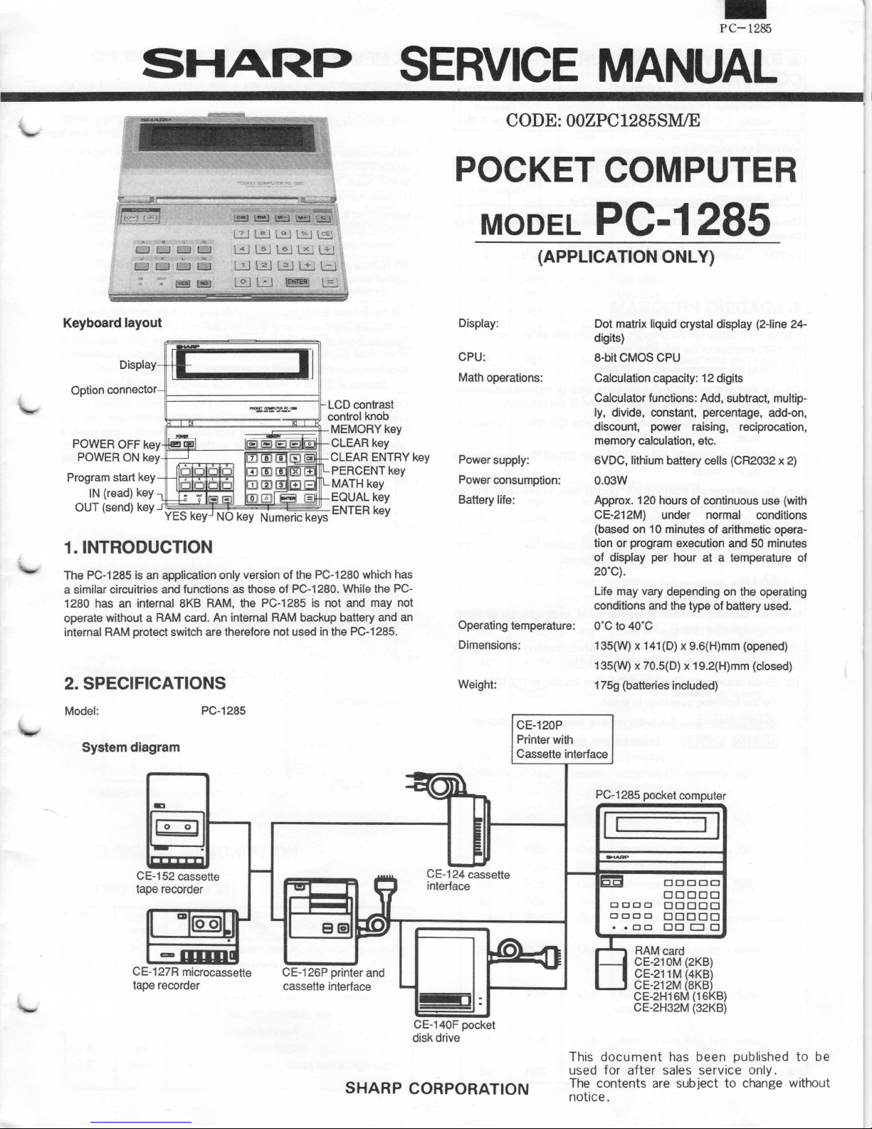
System diagram
CE-152 cassette
tape recorder
CE-127R microcassette
tape recorder
PC-1285
CE-126P printer and
cassette
CE-124 cassette
interface
interface
CE-140F pocket
disk drive
SHARP CORPORATION
CE-120P
Printer with
Cassette interface
PC-1285 pocket computer
This document has been published to be
used for after sales service only.
The
contents are subject to change without
notice.
,
..__I
_ ___.
eg DODOO
CJDCJD DODOO
DODD DODOO
DODOO
•CJCJ ODDO
RAM card
CE-21
OM
CE-211 M (4KB)
CE-212M (8KB)
CE-2H16M (16KB)
CE-2H32M (32KB)
(2KB)
Page 2
..
PC-1285
3. BATTERY LIFE AND CURRENT
CONSUMPTION
PC-1285 power Lithium battery
supply CR-2032 x 2 pcs
Capacity
170mAH
Current consumption
Current consumption when PC-
Current consumption when PC-
(with display on)
The above values are at the room temperature of 2o·c and may vary
depending on conditions.
(NOTE) Current shou
ld be measured wi
1285 OFF
1285 ON
th a RAM card loaded.
:
Terminal
voltage: 6.
45µA max.
450µA
max
0V
.
4. LOADING PROGRAM
A prog
ram
PC-12
85 in
eit
her of the following ways:
(1) Us
ing the
program stored RAM card
(2)
To load
progra
m from the cassette tap
the
followi
126P p
rin
ter/cassette interface or
ng opti
In this case,
G)
CE-
face
created on the programma
® CE-1
52
ta
(3)
To load pr
lowing option is
CE-140F (pocket di
cassette tape recorder or CE-127R mic
pe
recorder
ogram from the 2.5"
required
.
sk drive)
(4) To load program directly from another pocket
case, the following cable
EA-128C
NOTE:
Note the following when loading the RAM card wi
created or edi
(1)
(2) Erase reserve data by PC-
ted on the PC-
Set the PC-1280 in
1280
the
program. (Execute SETMEM "1" IENTERI .)
Do the following operation to erase
ISHIFTI IBASICI ...
[HJ~
&YI
IENTERI
Set
in
...
Erase reserve
ble
uni
t can be loaded
onto the
e or microcassette
on
G)
and® are
CE-1
requ
ired
24
cassette inter
.
rocassette
pocket disk. In
option is
required.
this case, t
comput
er.
th the program
.
MEM$="1" when creating or edi
1280 before
loading to PC-1285.
ting the
.
the reserve mode (RSV symbol on)
data
.
tape
he
fol
In this
.
-
-
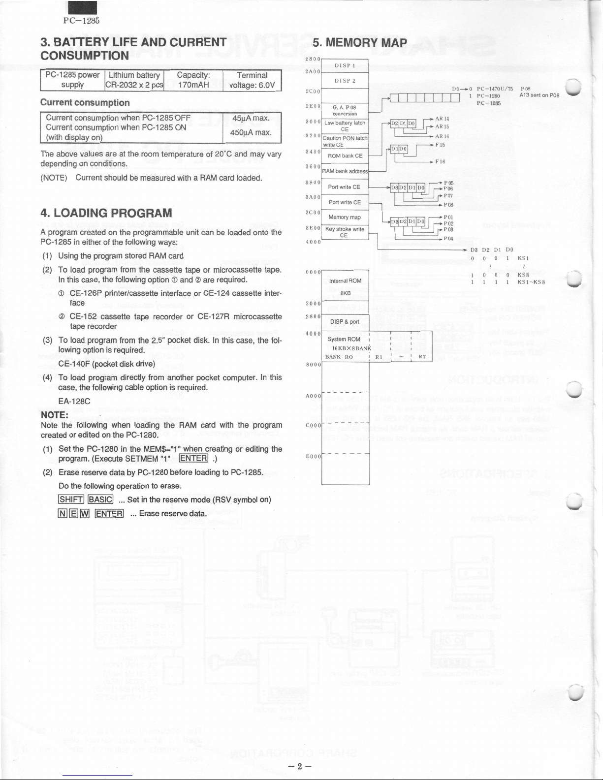
5. MEMORY MAP
2800~-
2AO Or-----_,
2COO
2EOO G.
3 0 0 O Low battery latch
3 2
3400
3600
38
00
3A
O O
3COO
3EOO
4000
00 00
20
00
2800
4000
8000
A
OO
co
o
EOO
DISP I
DI SP
APOB
conversion
C
O O
Caution PON latch
write
CE
ROM bank CE
RAM bank address
Po
rt
write CE
Port wr
Memory map
Key stroke wr
CE
Internal ROM
BK
DI
SP
S
ystem ROM
16KBX8
BANK RO
------
0
-
-----
0
----
0
--
E
ite C
B
& port
2
E
ite
BANK
-
-
....,
I
I
~
~-------
R
I
~~~~~~~
~---
L===
I
I
I
I
-
Do~o PC-1470U/75 P
I
PC-1280
PC-1
285
P05
P06
P07
-
POB
POI
P02
P03
:'..
P04
--+
D3 D2 DI
0 0 0
0 0 0 KS
I
I
I
I
R 7
OB
A13sentonPOB
DO
KS I
I
8
I KS!-KS8
-2-
,..
.
Page 3
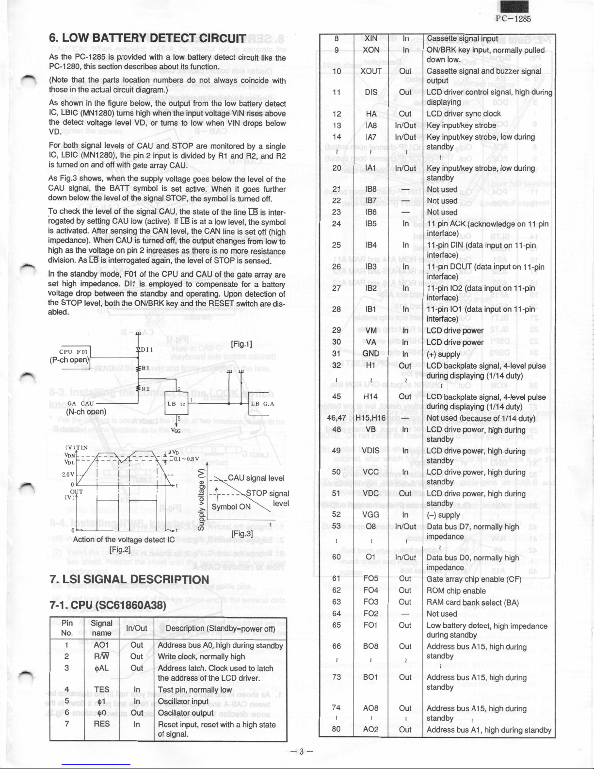
6. LOW BATTERY DETECT CIRCUIT
As the PC-
PC-1280, this
(
Note that the parts location numbers do not always coi
those
A
s shown in the
IC, LBIC (MN1280) turns hi
the detect
VD.
For both signal level
IC, LBIC
is turned on and off with gate array CAU
As Fi
CAU si
down below the
To
r
ogated by
is
activated. After sensing the CAN level, the CAN line is set off (high
impedance). When CAU is turned
high as the voltage on pin 2 increases as there is no more resistance
division. As LB is interrogated again, the level of STOP is
In
the standby mode,
set high impedance.
voltage drop between the standby and
the STOP
abled.
(P-ch
1285 is pr
in the actual circuit di
voltage level VD, or turns to low when VIN drops below
(MN1280
g.3
shows, when the
gnal, the BATT symbol is set
chec
k the level of the signal CAU, the state of the
setting CAU low (active
level, bo
CPU FOi
open)'!--
GA CAU
(N-ch open)
2.0V
-
O<-
-~-~~-
OUT
(V)
Q
b..__L__~
Action of the vol
ovided with a low battery detect circuit like t
section describes about its functio
agram
.)
figure below, t
s of CAU and STOP are mon
),
the pin 2 input is divided by
level of the
F01
011
th the
---
------'
L_ _
tage dete
[Fi
g.2]
he
output from the low
gh when the input voltage VIN ri
supply voltage goes below the level of the
signal STOP, the symbol is turned
). If LB is at a low level, the sy
off, the output changes from low to
of the CPU and CAU of the gate array are
is employed to compensate for a battery
ON/BRK key and the
DI!
~
RI
R2
---t--+
-'P
___L_.,
_
ct
IC
n.
.
active. When it goes further
operating. Upon detection of
RESET switch are
~
Cl)
Ol
~
-+
;:, Symbol ON
a.
Cl.
L__ _
::J
(J)
itored by a single
R1
_
- -
--
ncide with
batte
ry det
ses above
and R2,
CAU
and R2
off
line LB is inter
sensed
[Fig.1]
signal level
STOPsignal
[Fig.3]
.
mbo
.
dis
le
he
ect
vel
7. LSI SIGNAL DESCRIPTION
7-1. CPU (SC61860A38)
Pin Signal
No
.
name
1
2
3
4
5
6
7 RES
A01
Rfiii
cp
T
cp1
cpo
AL
ES
In/O
ut
Description (Standby-power off)
Out
Address bus AO, high duri
Out
Write clock, normally hi
Out
Address latch. Clock used to latc
t
he address of the LCD drive
I
n
Test pin, normally low
In
Oscillator input
Out Oscillator output
I
n
Reset
input, reset with a high
of si
gnal.
ng standby
gh
h
r.
state
PC-12
85
-
8
9
10 XOUT Out
1 1
1
1
14
20
21
22 IB7
-
l
-
23 IB6
24
25
26
27
28
29
30
31
32
45
46,47
48 VB
49
50
51
52
53
60
6
62
6
6
6
66
7
7
80
XIN
XON In
DIS
2
3
I
I
HA
IA8
IA7
I
IA1
IB8
I
B5
I
B4
183
I
B2
IB1
V
M
V
GND
H
I
H14 Out
H15
,H16
VDIS
vcc
voe
V
GG
08
I
1
3
4 F02
5
I I
3
4
I
I
0
F0
F04
F
03
F01
B08
B0
A08
A02
A
1
1
I
I
n
Cassette signal input
ON/BRK key
down low.
Cassette signal a
output
L
Out
Ou
In/
In/Out
In/Out Key input/key strobe, low duri
-
-
-
O
-
Ou
In/
In/O
5
Out
Ou
O
-
O
Ou
1
Out
O
Out
CD dri
displaying
t LCD driv
Out
Key
input/key strobe
Key
input/key st
standby
I
In
I
n
In
In
In
In LCD drive powe
In LCD drive power
I
n
ut LCD backplate signal, 4-level pulse
I
In
In
I
n
t LCD drive
In
Out
I
ut
t
ut
ut
t
I
ut
I
I
standby
Not used
Not used
Not used
11
pin ACK
i
nterface)
t t-
pin DIN (data input on t t-pin
i
nterface
t t-
pin DOUT (data
interface
t t-
pin 102 (data input on t t-pin
interface)
t t-pln 101 (d
interface)
(+)supply
during di
I
LCD
during displaying (1/
Not used (because of 1 /14 duty)
LCD dri
standby
LCD drive
standby
LCD dri
standby
standby
(-)s
upply
Data bus 07,
i
mpedance
I
Dat
a bus DO, normally high
im
pedance
Ga
te arr
R
OM ch
R
AM card bank sel
Not use
Lo
w battery det
duri
ng st
Addre
stan
dby
I
Address bus A 15,
standby
Address bus A 15,
standby
Address bus A1, high during standby
input, normally pull
ver
control signa
er
sync cloc
(acknowled
)
)
ata input on 11-
splaying
backplate
ve power, hi
power, high during
ve power, high during
power, hi
normally hi
ay chip enable (CF)
ip
enable
d
andby
ss
bus A 15, high
I
ed
nd
buzzer si
k
robe, low duri
inpu
r
(1 /14 duty)
signal, 4-level pulse
14 duty)
gh during
gh
ect (BA
ect, high impedanc
high
high during
gna
l,
high durin
ng
ng
ge on 11
t on t t-pin
pin
durin
g
gh
)
durin
g
during
l
pin
g
e
-3
-
Page 4
~
PC-1285
7
-2. Gate array (LZ92K41)
Pin
Signa
l
I
C
LB
1
I I
A9
I
In/Out
In
Bank selec
I
n
Chip enable
In
Data bus
I
In
D
In
(-)supply
Out
11-pin
Out
11-pin 102
Out
11-pin DOUT (P-channel open
output)
Out
11-pin DIN (P-
Out
11-pin BUSY (P-
output)
-
Not used
Out
Not used
Out
Not used
Out
System ROM A 14 and RAM A
Out
System ROM A 15 and RAM A 12
Out
System ROM A16 and RAM A13
Out
RAM card slot A1
RAM card A16
O
ut RAM card sl
Internal RAM chip
Out DISPCHIP1 chip enable
DISPCHIP2 chip enable
Reset output to
normally low
O
ut
ON/BRK output to CPU KON line,
n
orma
In
Low battery detec
I
n
Reset
In
ON/BRK k
down
In
(
+)supply
(-)supply
voltage
after acti
Out Key strobe (P-channel open
In
Write clock
In
Address bu
I
A
No
.
n
ame
1
2
3
I
6
(
7
8
9
10
11
1
2
13
14
15
16
17
18
19
20
2
1
22
23
24
25
26 KON
27
28 RES1
29 BRK
30
3
1
32
33
I
40
41
42
I
48 A15 In
BA
CE
DCO
D03
GND
P01
P02
P03
P04
P05
N
SLTB
AS3B
AS1
AS2
AS3
AF15
AF16 Out
SLT1
SLT2 Out
DSP1
DSP2 Out
RESO Out
Voo
GND In
CAU Out Low battery symbol
KS
KS8 Out Key strobe (P-channel open
R/W
D
escription
t
I
ata bus
101
(P-channel open output)
(P-channel open output)
channel open output)
channel open
5
ot chip
ena
enable
CPU RESET line
lly low
t, low at low
input, normally pulled down
ey input, normally pulled
detect line, high impedance
vation of
I
s
I
ddress bus
activating
symbo
ble
l.
11
,
batte
outpu
output
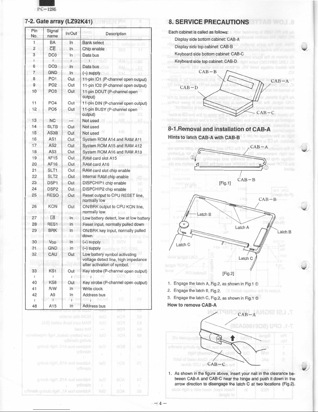
8. SERVICE PRECAUTIONS
Each
cabinet is
D
isplay
Display side top cabinet: CAB-B
Keyboard side bottom cabine
Keyboard side top cabin
C
8-1.Removal and installati
Hints to
calle
d as
follows
:
side bottom cab
AB-D
latch CAB-A
®
/~=::::::::::::::=::::::::::::::~~
~==~~~~~
inet: CAB-
et: CAB-D
A
t: CAB-C
with CAB-B
on
of CAB-A
CAB-A
=~~
CAB-
A
I
C
g.2]
AB-B
Fig.
Fig.1 ®
Latch
B
1
G)
[Fig.1]
ry
t)
)
1. Engage the lat
2. Engage the latch
3. Engage the latch C, Fig.2,
How
to
remove CAB-A
ch A,
B,
[Fi
Fig.2, as shown in
Fig.2.
as shown in
1. As shown in the figure
tween CAB-A and
arrow direction to disengage the latch C at two locations
-
4-
above, i
nsert your na
CAB-C near the hinge and push it down in
il in the clearance be-
(Fig.2
the
).
Page 5
2. Do the reverse sequence to remove the latches.
CAUTI
ON: When removing CAB-A, be careful not to separate the
static tape.
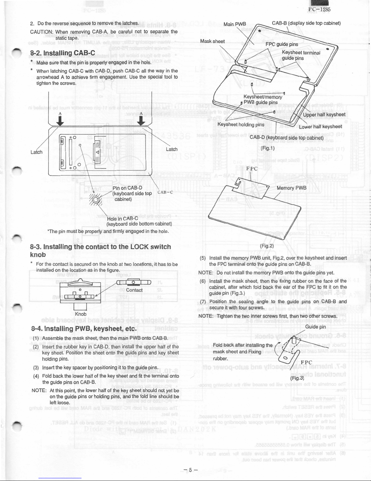
8-2.
Installing
*
Make sure that the pin is properly engaged in
*
When latching
arr
owhead A to achieve firm engagement. Use
tight
en the
CAB-C wi
screws
CAB-C
th CAB-D, push CAB-C
.
the hole.
all the way in the
the special
..
PC-1285
Mask sheet
tool to
l
t
Latch
~[
/
/
~
*
The pin must be properly and firmly eng
8-3.
Installi
knob
*
For the contact
i
nstalled on the location as in the
ng the c
is
secured on the knob at two locations, it has to be
Q;Y'
Knob
[
I
/,?(ke
yboard
{(
/
ontact
~J
PinonCAB-
c
abi
H
ole in
(key
board side
to the LOCK switch
figure
D
si
net)
CAB-C
aged in the hole.
.
(?1 ll
Contact
de top
bottom cabinet)
CAB-c
Latc
Lower half keyshe
CAB-D (keyboard side top cab
(Fig.
h
FPC
(5) Insta
NOTE: Do not install the memory PWB on
(
(7) Posi
NOTE:
ll
the
memory PWB unit, Fig.2, over the keysheet and insert
t
he FPC
terminal onto the gui
6) Install the mask
cabine
t,
after which fol
guide pin
secure it with
(Fig.3.)
tion the sealing angle t
four sc
Tighten the two in
sheet, then the
1)
(Fig.2)
de pin
s on CAB-B.
to the gu
d back the ear of the FPC to fit it on the
rews
ner screws first, th
fixing rubber on the face of the
o the guide pins on CAB-B and
.
en two other
inet)
ide pins
yet.
screws
et
.
8-4. Insta
(1) Assemble the mas
(2)
(3) Ins
(4)
NOTE: At this point, the lower half of the key sheet should not yet be
lling PWB, keysheet, etc
k sheet, th
Insert the rub
key s
holding
ert the key spacer by
Fold back the
t
he guide pi
on the guide pins or holding pins, and the fold line should be
left
ber key in CAB-D, t
hee
t.
Position the shee
pins.
lower
ns on
loose
.
CAB-B.
en the main
hen
t onto the gui
positioning it to the guide pins.
half of the key sheet and fit the terminal onto
install the
.
PWB onto CAB-B
upp
de pin
er half o
s and key sheet
.
f the
-5-
/
(Fig.3)
G
uide pin
Page 6

PC-1285
-
(Fig.4)
(8)
Solder the buzzer leads to the
A) as shown in Fig.4.
t
ape with a tapping screw. A
(9)
Latch CAB-A with
(10) Close the unit halfway (Fig.6) and install the lower
and the memory PWB on CAB-D.
(11) Install CAB-C.
CAB-B.
display-side bottom cabinet (CAB-
Next, fasten the
lso sc
terminal lug of the
rew the other
one. (Fig.5)
hal
f key sheet
static
8-8. Hints and
• Any parts must be closely attached on the PWB with solder.
• When replacing
Service Information PS-009.)
• See the figure below for the installation of a 0.
the KON (pin 26) of the gate array and the VGG side of a 0.033uF.
• The capacitor inserted to the 11-pin
the following ma
tips
LSls, use the ALUMIT KR19RAM
1uF insert
connector must be installed in
nner.
solder. (See
ed across
v
-
(Fig.5)
(Fig. 6)
8-5. Re
The static
be used again. A new one must be
pan
check ground continuity in accordance with 8-6.
8-6. Ground
Check that the resistance between the display side
and the RAM card lid is not more than 5 ohms
8-7. Internal RAM
placing the
tape, once
el before attaching a new static
continuity
static tap
sepa
rated from the al
check
capacity
e
uminum
used. Wipe residual glue off the
tape.
panel, should not
After the
cosmetic
.
replacement
and auto-power
functional checks
The contents of the memory will be erased wi
dure.
(1) Insert the RAM card.
(2) Press the RESET switch
(3) Press the YES key.
but the YES key ON prompt
tents of the RAM
(4) Key in
(5) The display will show
(6)
[[)Gill:JGJ
After leaving the unit in the above state for more than 14
minutes, check tha
.
(Normally, the YES key may not be
may
card.)
.
0.55555555555.
t the power has been out.
th the
following proce-
appear depending on the
pane
off
pressed
con
• Pro
vide the following 1 O OQ r
esisto
r.
~
I
.
8
~I
•
Providing jumpe
J1
J2 105
J3
,
r
Length
140
12
7
w
PWB unit
Main
PWB
Mem
ory PWB
8-9. Display side cabinet and keyboard side
cabinet
These two cabinets are held together with a spring
ei
ther on
l
ter a
pulled out, cannot be
e only, it
nd to remove the spring pin with a pai
8-10. Display
Items
required for display ch
•
PC-1280
•
Half-size RAM card (for test)
•
PC-1285 to be tested
The contents of both PC-1280 and the RAM card will be los
t
,
-
he test.
(1)
Set the RAM card in the PC-1280 and do ALL RESET.
(
2) Enter SETMEM"1"
(for pr
may
re-used
test
ogram
be pos
sible to scrape the cabinet with the
.
eck
:
entry
)
[:;;D
.
r of pliers, but the
pin. To replace
cut
pin, once
t during
-
-6-
Page 7

(3)
Enter the following
"8".)
10: "A"
20 :
WAIT20
30 : BEEPl
35 :
IF INKEY$="0"THEN60
40: PRI
50: IF
60 :
70 : PO
80 : GO
(4) Turn power off the PC-1280 and s
1285.
(5) Turn power on and press the
(6) Check that the figure "8"
row and the second row. Make sure that "8" on the se
begin to disappear one by one.
(7) Press the
(
8) Press the I ON I key
(9) Press thelOFFI key.
NT"8-8";
INKEY$<>"0"THEN30
POKE&237c, 255, 255
KE&283c, 255, 255
TO
[Q]
program. (
80
is
displayed in every digit on the first
key. (About 1 second)
.
On the line 40, enter 23 digits of
et the
RAM card in the PC-
[Al
key
.
cond row
9. CHECKING WITH THE TEST PROGRAM
A test program
Test items
(
1)
RAM card read after write test
(
2) 11-pin connector 1/0 line test
(3) 15-pin connector 1/0 line test
NOTE: The item (3)
Tool required
The PC-
fo
r (2) and (3).
Description
The RAM contents will be erased in the progress of the test item
N
ecessary program and data must be saved on on tape or other
device before starting the test.
is
contained in the ROM.
is
not used for PC-
1360 special tool UKOGC3020CSZZ (price rank: BC)
1285.
(Power OFF
Turn power on while holding down the
following three keyssimultaneously.
IBllRJ
IIDITI
is used
(1 ).
Details of test
(1) RAM test
Refer
to
NOTE
3,4
NOTE 3: For PC-1285, enter
NOTE 4: The RAM contents will be erased during the test. (To
item
s
Men
u
[I]
IA],
(
RAM!)
X
WAl'f'#.
(
RAMI
)
ERROR OCCU
. (RAMl)
(????H-????H
IENTERI
(
RAM2) B:4K D:16K
A=2K c:aK J:32K
rxi
lllh Wh ~.
(RAM2)
XWAl'f'#.
ERROR OCCURED AT
(
RAM2
)
(
????H
-????H
I
Menu
AM2.
preserve the
contents,
D
:16K
C:SK
J:32K
IB],
[CJ.
RED AT ????H
IS CHECHED)
rm
17'1
IS
CHECKED)
ENTER
I
[IS]
to pass the test item
enter
ID!
.
IT'\!
rn
1.1.!1• l.SLJ
[R]
to pass.
K:PASS
Q]
I
ENTER
K:PASS
Refer to
NOTE 3
IENTERI
????H
I
(2)
NO
11·
Te:
~
NOl
QI
(
MENU>
l:RAM 2:;;
I
,
NOTE 1:
NOTE
Power can be
the display.
2:
If
the te
PIN 3:
Enter
[TI
,___
Enter
[g)
,_______
Enter
~
Pow
er
off
'-----
st program fails to st
-+(Power OFF)
turned o
15PIN
(1) RAM te
(2) 11-pin test
(3)
15-pin test (not nece
ff only when the
I
st
art, check the
for PC
abo
ve
keyboard
ssary
-1285)
menu is
first.
on
-
7-
Page 8

(2) 11-pin test
Fasten the 11-pin connector of the test too
face up,
to the t t-pin
connector on the le
Menu
[ID
(
llPIN
)
"lf.WAIT"lf.
(
llPIN
)
XOUT:HIGH
(
llPIN
)
CHECKED
jENTERj
Menu
NOTE
1:
The tes
t pins and the test sequence are shown next.
ft si
XIN:LOW
l,
with the parts si
de of PC-
1285.
jENTERi
de
10. LCD WIRING SCHEMATICS
PC-1285
-
the t
est. (To
I
p
MT2
c;N!)
V
GG
BUSY
I.>OUT
XI
N
XOUT
ll!N
A
CK
10
2
101
UCNCMI 307CC!
Test tool t t-pin connector
circuit
diag
ram
NOTE 2: No error will be found if
lines insi
IOOKO
H
de the unit.
there was a
XOUT-+XIN
CD
101-+102
®
@
102-+101
DOUT-+DIN
©
@
DIN-+DOUT
BUSY-+ACK
<ID
sho
rt between si
gna
l
S56--
S5
7
S58
S59
S60
-8-
Page 9

PC-
-
11. CIR
128
5
CUIT DIAGRA
'---
1-
7
H
M
L
F-7318E
CL
CD)
f
.........
H8-14
5
'-
'-
~
-
:::
....___
---~
....._~
....._~
r---
r--~
~
r---~
"----~
1'--...§.ll
4
fil
~
~:
~
~
~
~;~
1
n
un
j~~
~
lol1>I
CJ1
r--111:111D1•
..
II) In
..,
IMIN
SC43536
~l~
g
<1
~~
~~UI CD~
vi inJ:lo•
a::uoo
J J
r
r r r r r
olc>
m
lnl
U»l
lnlll>llln
CD I SP
m<>•
"'"
!~~11
000
>l;l:l:J
l
Oleo
;
r
Wi--.
•
'Si"e---
um-
SIB!---'
~---
514 ___.
ID>-·
.fill.___.
~
-
~
I--
~ =~
I
)
rs-7~
:J
n~
TI~
l:1~
CID
82
_L
-~
0P
~
~~
r"-
r---'$':49
~
f\--
~
l'--'555
r---~
r-'557
C
L)
~rm
~
:~
~
~
~
:~:
l l
lrrl.
N-ld
o-1m1,......tn111"11
..
SC
I~~~
"'-ti"
<le <'II'!
:::c
l
... 1-
N1-io ~
43536
CD I SP2
IQ•"'
I•,.
•le
le
+
trOO
l
olol<
;
J
r r
1~:J
1E>lt>\.,l
NN
N
U)
"'
lll>lln
N-
0 • NSJ
0
10 ~
!1;;; II) Ill Vl
I J
f'J!N
lnllnt"'101"-
)
l
~Id
•
i.!.LQ.L........
~
~'--'
un-
tH>-
m
~
51
8~
m~
..fil_!
i--'
SI!)
L....-o
:!:t!
~
Sl~i--'
~~
~L........
I---
s
7
L-..
L-..
VRI
20K
c:=
RESET SW
0.033·
C
8
RB
<>---
:t---
v
V
IOOK
-
~
.._____
.._____
~
Ceramic ca
[
3
~~
..--
SL
OT
GNDJ.
Vee
R/W
_
__,
A
0
__,
A I-
_
__,
_
__,
A 2
A
3
f-__,
A
4
,____,
A 5
f-__,
A 6
A 7
f-i-'
A 8
,____,
A
2
9
AIO
A
I I
Al2
Al3
Al
4
Al5
Al6
NC
N
C
D
0
D
D 2
D
3
D
4
D 5
D
6
D
C
E
NC
N
C
O
E
VG
G
f-f--'
-·'-"'
,__
-
-
~
I
~
~
r----'
~
'------'
'------'
7
11
35
1
,
I
lOO
11
KO Y4W}
lo'-
I,-
,
_
-
~
l<l<I
LJ
LH5310X
i
1
~1~~
[
'"
"JJ
CROM)
~~~~1
L
~Tl"1
9
.~
I~~~
L
lti
E
v
~
~
pacitor
CllO.l•r1f-
l
<nVHl'lVJ<
1·3l">!l"J!
J.1.:J.J.l.:J.
I'-~
r--
J:.S
6
r--
757
....__
~
R
/W
r-7:9
v----
TIO
~~
It- AIS
~m
v--
[!I]:
•
<
1~ 01e
11
!g
LZ92K41
CG. A)
w15
gg1~~
I
I
l
I
1Jai
A 12 Al 3
39~.c.G~.5
~J~
0
3 MN
osr s
a
CS
P
O
SPI
[5lf;
S
L t 1
A
FI
AF
I
A
S3
~
.__
a!!!.
~
~
,tLl..
I
15 0
280
PCH
)
•.
SK CG)/'""'\
~
0
2
ISRl
\J
4B
~
e
with
A
Diod
n
o
comment
DAN202K
IS
B
c
D
-9-
Page 10

GND
HB-
RES
14
VRI
ET SW
CB o.033•
RB
20K
IOOK
VA
VM
VB
VD
!
VGG
5
5BK
s
CCPU)
C2
l
u
A38
_l
C R2032*2
VG
+
3.3
Cl
u
RI
10
5
DI
I
A6
IA7
!AS
KSB
R7 I OOK
I
OOP
C5
J:OP
EX:SHORT
CH)
EN
I
OOP
C
B
XI
RB
I
M
CH)
CSB7
BB
4
3
L---
J
06 DA204K
r-----
,
I
r-~+-........,1--f-+-+~~~--,
DTAI
1-;(
I
--
H
E
:DT2
~
~-r-~~~
1DT3
I
I
_.J
•3
F
-
10-
2
RI I
I
OOK
G
0.
1µ•
2
F·(i-
Ceramic capa
I
I
MT2
G
VGG
BUS
Da
X
x
DIN
AC
1
10
I
ND
ul
IN
oor
I:.
02
1
citor
Pi n
Y
H
Page 11

12.
PARTS SIGNAL LAYOUT
Main PWB parts side
RAM slot PWB parts side
Route within these two lines
4
~
M10
*
Take care not to pinch the jumpers J2 and J3 when
engaging the
54
cabinets
Route within these two lines
)
-11-
Page 12

Main PWB LCD side
PC-1285
-
hin these two lines
J
r
~ -
ssczz
R
AM
slot
PWB key side
(
1 .
2mm
height MAX
No pattern
)
0
-12
-
Page 13

PC-1285
-
13.
PARTS LIST & GUIDE
[I]
Exteriors
NO.
2 PFiLW100
3 P S H E Z 1 0 1 9 E C S
4 DU
7
8
9 QCNCW1306CC1
10
11
12 P T P E H 1 2 1 3 C C Z Z
13 PTPEH1026EC
14 DUNT-1267ECZ
15
16
17 LX-BZ1200CCZ
18 DUNTG1265ECZZ
19
2
0
21
22
23
24
25
26
27
28
29
30
31
32
33
37
38
39
40
41
42
43
45
46
47
48
49
PARTS COD
1
DUNTG1263ECZ
PGUMS1017ECZ
CPWBF1052EC0
LX-B
RALMB1030CC
PGUMM1015ECZ
LANGTlOllECZZ
GFTAS1282C
DUNTG1262EC
L P i N S 1 0 0 2 E C Z
PGUMM1020ECZZ AH
P Z E T L 1 0
CPWBF1053EC01
MSPRC1016ECZZ AA
MSPRClOOlECZZ
0CNTM1042CCZZ AA
MSLiP1003ECSA
PGUMM1594CCZZ
PGUMS1608CCZZ AE
GCABA1030ECSA AE
PZETL1564CCZZ
QTANZ1503CCZZ
LFiX-1190CCSE
P Z E T L 1 0 3 1 E C
GFTAU1012ECSA
0TANZ1406CCZZ
LX-BZ1030ECZZ
LX-BZ1029ECZZ AA
L
TLABZ2240CCZZ
TLABH116
PGUMS1021ECZZ
TLABZ1008ECZZ
TLABPl 165ECZZ
9ECZZ
NTK1227
X-B Z 1 1 4 0
ECZZ
Z1155CCZZ
2 7 E C Z Z
1EC
Z
3
B
ZZ
ZZ
E
Z
Z
Z
Z
Z
Z
CSD
ZZ
Z Z
EC Z Z
PRI
CE
NEW PART
RANK
MARK RANK
AP
AD
A
AA
AV
A
BQ
AK
AA
AD
AB
AE
AK
AB
AC
AA
AR
AB
AM
Z
AA
AA
A
AB
AB
AB
A
AB
A
A
AE
AB
AA
AA
AA
A
AA
AA
AA
N
0
Too cabinet unit (Disolav side)
Polarized filter
c
N
c
Mask sheet
B
B
N
N
N
N
N D
N D
N
X
N
N
N
B
B
N
C
N
N
N
N
A
N
LCD unit
c
R
ubber connector
E Ma
in PWB unit
Connector
c
Screw (2X3.5\
c
B
Buzze
r
Taoe
c
c
Taoe
B
Kev unit
Fixinz rubber
c
Fixin11
c
c
D
c
B
c
E
c
c
c
c
c
c
D
c
c
D
c
D
c
c
c
c
c
c
c
c
c
anzle
Screw
Bottom
Lid(for connector)
Too cabinet unit (Kev side)
Sprin11
Key
rubbe
K
ev
space
Memory PWB un
Sprin11(fo
PS so
rinz for RAM card
Slide swi
Slide
switch knob
Reset
sprin11 rubber
Rubber connector for RAM card
Bottom
Insulat
or
Batte
rv termi
Ca
rd stoppe
Insulator sheet
Lid for ca
Batterv term
Screw
(2
Screw
(2 X
Screw
Batterv cover
Cauti
on
Cu
shion(for LCD
Caution labe
Batterv
(No.9t~t;)
(12oin)
cabinet (Display
pin
r
r
it
r lid)
tch termina
cabinet
(Kev s
shee
t
nal
r
rd
inal (HJH\
X
6
.8)
4.8)
labe
label(B
atterv re
)
l
labe
l
l
A
l
side
ide)
placement
DESCRIPTI
)
)
ON
(Include
(Include
No.11
No.
-13)
25 26)
• Battery ®8
inc
-13-
*
'Mien
attaching
fall into the slit sho
•
CAUTI
ON
label
Page 14

•
Battery 8;18
ch. the
~II
::nth~t:lit
l~~own in the
• CA
UTION label attachment (
l
indication label position
label,
be
careful not to
figure.
RAM
50
card
:
~~
section)
49
48
21
~-----
38
I
~
47
-14
-
Page 15

PC-1285
-
2
-
ain PWB unit
PARTS CODE
! QCNCW1306CC1
: RC
-CZD105E
l RC-CZ1047CCZZ
~
RC-
EZ335BECOJ
RC-
KZ1054CCZZ AB
6
R C R S Z 1 0
8
RH-DZ 1001ECN1 AD
9
RVR-
10
11
12
l3
1
4
15
i
s
17 VH i LZ9 2K4
18
19
2
0
21
2
2
2
3
24
25
26
27
28
29
30
31
32
901
Z2400QC
V
CCCTP1HH101J
V C K Y T P 1 E F 1 0 4 Z
V
CKYTP1HB821K
VHDDAN202K/
VH
DDA204
V H i L H 5 3 1 0 X 9 - 1
VHiMN1280Q
VHiSC43536
VHiSC61860A38
VRD-HT2EY104J AA
VRS-TP2BD100J AA
VRS-TP2BD104J AA
VRS-TP2BD105J AA
VRS-TP2BD203J AA
VRS-TP2BD39
VRS-TP2BD472J
VRS-TP2BD562G AA
VRS-TP2BD563J AA
VSDTA144EK
VSDTC144EK
VS2SC2412K
CPWBF1052EC03
B
6 3
ZZ AF
K//-l AC
1/-
/-
/-l
I Unit)
PRIC
RANK
CZZ
C C
Z Z
-l AB
1
1
3G
/
-1
/
-1 AC
/
-1 AB
AK
,
A
AB
A
A
AA
A
AA
AW
AN
AE
AX
AX B
AA
AA
AC
BQ
E
NEW
MARK RANK
C
B
F
A
PART
c
c
c
c
c
B
B
B
c
c
c
B Diode (DAN202Kl
B
N
B
N
B
B
B
c
c
c
c
c
c
c
c
c
B
B
B
N
E
Co
nnector (12oinl
C
aoacitor (luFl
C
aoacitor (0.
Capacitor (6.3WV 3.3uF)
Caoacitor (50WV 0.
Crvstal (76SKHz
Diode OSR14Sl
Variable
C
apacitor (50WV lOOPF)
Caoacitor (25WV 0.lOu
Caoacitor (50WV S20PFl
Dio
de
IC (LH5
IC ILZ92K41
IC
IMN12SOQ)
IC CSC
IC (SC61SOA3Sl
Resistor
Resistor fl/SW
Resistor (I/
Resistor 11/SW I.OMO ±5%1
Resistor
Resistor I
Resistor 1 1/SW 4.
Resistor I 1/SW
Resistor (l/
Transistor IOTA 144EKl
Transistor
Transistor (2SC2412Kl
Main
033uF)
l txn
resistor (20K(l)
(DA204K
l
310X9)
)
43536
l
(l/
4W lOOKO ±5%)
SW
1/SW
20KO +50/-1
I
1/SW
39KO
5.6KO ±2%1
SW
56KO ± 5%
CDTC144EKl
PWB unit
luFl
Fl
100 ±5%)
lOOKO ±5%1
±2°/nl
7KO ±5%1
DESCRIPTION
l
[C2
[CS]
[Cl]
[
D2]
[VRl]
[C5
[C34
[ClO]
[D1457S]
[DG]
[ROM]
rG
·A]
[
DISPl,2
[CPU]
f
[R6710,11]
Rl
[RS]
[
R34]
[R12]
[R9
[R13
[R2 5]
[DTl-3]
[
DT4]
[01]
]
6]
71
]
]
]
]
~
Packing material & Accessories
NO.
1 L P L T P 1 0 0 8 E C Z
2
3
5
6
7
PARTS
PHOG-1001ECZZ AA
T i N S E
TiNSE1135ECZZ AU
T i N
S E
TLABZ1153ECZZ AA
SPAKC0316ECZZ
SSAKH3013CCZZ
CODE
1 1 4 6 E C
1 1
3 6 E C
PRICE NEW PART
RANK
Z
AD
Z Z
Z Z
AQ
AU
AG
AA
MARK
RANK
N
N
N
N D
DESCRIPTION
D
Temolate
D
Cushion oaoer
D
Instruction book
D
Instruction book (for Germanvl
D
Instruction book
Label
c
Packing case
D
Vinvl baz
(for Other countries)
(for U.S.
A.)
-15-
Page 16

PC-1285
-
SHARP
COPYRIGHT © 1988 BY SHARP CORPORATION
All
rights reserved.
No part
electronic, mechanical,
without prior written
of
this
stored in a retrieval system, or
in any
Printed in
publication
form
photocopying,
Japan
.
may
be
reproduced,
transmitted,
or by any means,
recording, or otherwise,
permission
of
the publisher.
SHARP CORPORATION
Information Systems Group
Quality & Reliability
Yamatokoriyama, Nara 639-11, Japan
1988
August Printed
Control Center
in
Japan
($)
 Loading...