LZ93N61
LZ93N61
DESCRIPTION
The LZ93N61 is a CMOS timing generator LSI
which provides timing pulses used to drive a
CCD
area sensor, in combination with the SSG
LSI (LZ93NI 9, LZ93B53).
FEATURES
●
Switchable
320000 pixels CCD
●
Switchable between NTSC
(CCIR)
●
Internal electronic shutter :
Shutter speed is selectable from 1/W, 1/125,
1/250, 1/500, 1/1 000, 1/2 000, 1/4 000 and
1/10 000 s, in addition to this, 1/100 s (PAL
: 1/120 s) in Flicker-less mode using parallel
or serial code. Shutter speed can also be
controlled in 1 H period using an external
trigger to the EXST input.
c
Single +5
●
Package : 48-pin
between 270000 pixels
systems
V
power supply
QFP(QFP048-P-I
(EIA)
CCD
and
and PAL
01 O)
Timing Pulse Generator LSI for CCD
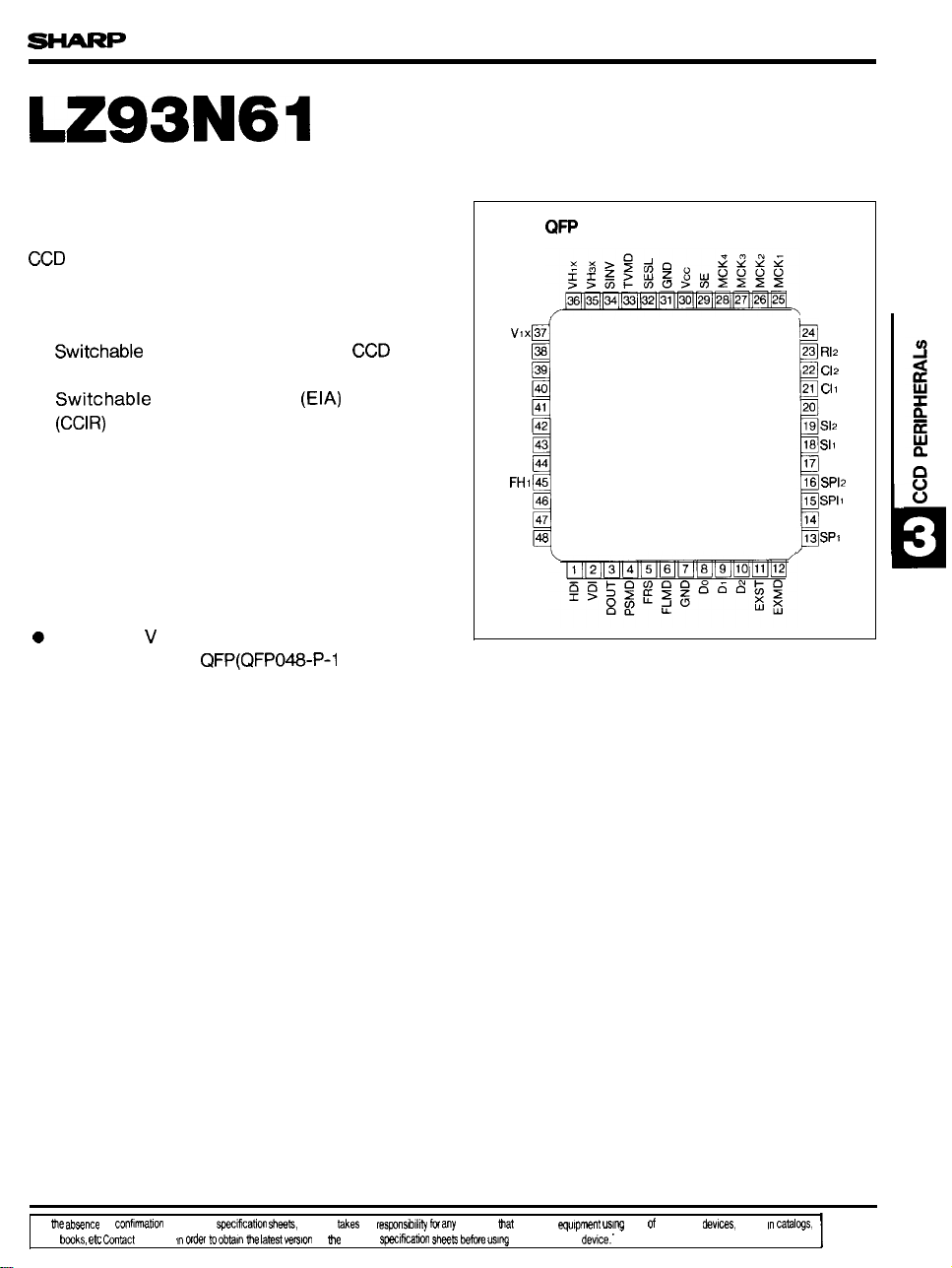
PIN CONNECTIONS
48-PIN
Vlx
V2X 3a
V3X
V4X 40
OFDX 41
FR 42
GND 43
FH2 44
FHI 45
CKI 46
CKO 47
TSTI
QFP
37
39
W
o
I
TOP VIEW
24 R12
23
R12
22
C12
21
CI1
20 FCDS
19
S12
18
SI1
17 FS
16
SP12
15
SPII
14 SP2
13
SPI
1
“In
deta
tie
abeence
bwks, etc
of
conf[mtlon
hn~ct WARP !n
by device
acecification ehwf?,
mder to obtain
tie
Iateat vefilon
WARP
fakee
no
of he device swIkaiim
reswns!blhty b
anY
defects
shw~ ktie USIW
hat
recur In
qutpment USIW
any 8HARPs
dewce.”
any of WARPS
davIces,
show In
Cahlws,
I
287

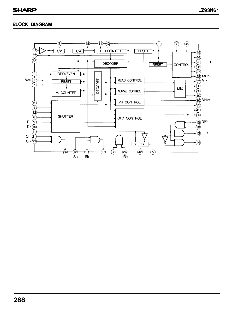
LZ93N61
CKI
CKO
TVMD
VDI
Vcc
GMD
FLMD
PSMD
EXMD
EXST
Do
DI
D,
Cll
C12
DOUT
FCDS
S1,
TST
S12
I
GND GND
FS
RI I
R12
FR
FRS
HDI
SESL SINV
FH
I
FH2
MCK
MCK2
MCK3
MCK.
Vlx
V2X
V3X
V4X
VHIX
VH3X
OFDX
SE
SPI 1
SPI 2
SP
1
SP2
I
288

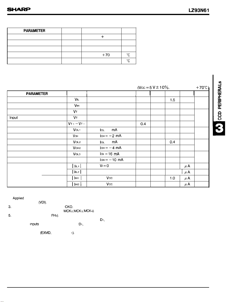
ABSOLUTE MAXIMUM RATINGS
PARAM=ER
Supply voltage
Input voltage
Output voltage
Operating temperature
Storage temperature
SYMBOL
Vcc
VI
Vo
Topr
Tstg
RATING
– 0.3 to
+ 7.0 v
UNIT
–0.3 to Vcc + 0.3
– 0.3 to Vcc + 0.3 v
–20 to
+70
–55 to +150
LZ93N61
v
“c
‘c
DC CHARACTERISTICS
PARAMHER
Input Low voltage
Input High voltage
Input High threshold voltage
lnDut Low threshold voltage
Hysteresis voltage
Output Low voltage
Output High voltage
Output Low voltage
Output High voltage
Output Low voltage
Output High voltage
Input Low current
Input High current
NOTES :
Applled to
1.
2. Applied to
3.
Applied to
4. Applied to
5,
Applied to
6. Applied to
7. Applied to
8. Applied to
9. Applied to
all inputs except for VDI, CKI.
input
(VDI).
all outputs except for
outputs (FR, MCK I,
outputs (FH 1,
FH2).
all inputs except for PSMD, FRS, FLMD, Do,
Inputs
(PSMD, FRS, FLMD, Do,
all inputs except for EXMD, TVMD, TST
(EXMD,
inputs
TVMD, TST
~
SYMBOL
VIL
[
I
vlH
vT +
vT -
vT+
–VT-
VOLI
vOH
1
vOL2
vOH2
vOL3
v0H3
I IIL1 I
I IIL2 I
1
tlHl
I
I IIH2 I
CKO.
MCK2, MCK3, MCK4).
D!,
D2, EXST, SESL, StNV).
I).
CONDITIONS MIN.
IOL
= 4 mA
IoH=–P
mA
IOL
=8 mA
IoH=–4
mA
IoL=16
mA
IoH=–10
Vl=o
mA
v
Vl=o v
VI= Vcc
VI= Vcc
DI,
D2, EXST, SESL, SINV
1.
(VCC=5 V~l OYO.
]
1
TYP. I MAX.
Ta=–10 to
1.5
3.5 v
2.2
1,0
3,8
2.4 v
0.4
0.4
4.0 v
0.4 v
4.0
0.4
4.0
1.0
8.0
60
1.0
8.0 60
UNIT
v
v
v
v
v
v
v
PA
\ AA
PA
PA
+70”C)
I
NOTE
1
2
3
4
5
6
7
8
9
289

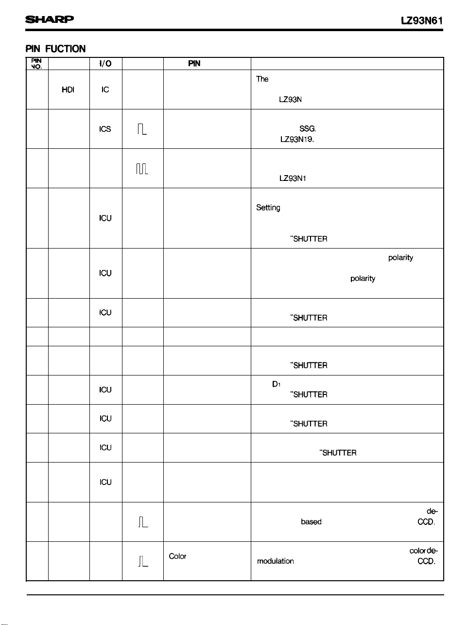
LZ93N61
~:.
SYMBOL
1
HDI
2
VDI
3 DOUT
4 PSMD
FRS
5
6
FLMD
7
GND
1/0
POLARITY
Ic
Ics
o
Icu –
Icu –
Icu –
— —
MM
n
nn
PfN
NAME
Horizontal drive pulse
Vertical drive pulse
Delay-Line clock
Shutter mode select
input
FR control input
Flicker-less mode
select
Ground
FUNCTION
Ths
HDI pin is used to input the horizontal reference
signal from SSG. It is connected to the HD (pin 31)
I-Z93N
of the
The VDI pin is used to input the vertical reference
signal from
of the
The DOUT pin output 1/2 dividing clock input to
the CKI (pin 46). It is connected to the CLKI (pin 27)
of the
The PSMD pin is used to switch the Shutter Speed
%tting
(Refer to
The FRS pin is used to selects the
FR (pin 42).
The FLMD pin is used to prevent the flicker.
(Refer to “SHU~ER MODE TABLE ”.)
The GND is a ground pin.
19.
SG.
It is connected to the VD (pin 34)
U93NI 9,
~93Nl
9.
mode.
High level : Parallel Setting mode
Low level : Serial Setting mode
“SHU~ER MODE TABLE”. )
~larity of the
High level : negative ~larity
Low level : positive polarity
6
9 D
10
11
12
13
14
290
Do
I
D2
EXST
EXMD
SP1
SP2
Icu
Icu
Icu
Icu
Icu
o
o
Shutter speed
—
switching input O
Shutter speed
—
switching input 1
Shutter speed
—
switching input 2
Shutter speed
—
control 1
Shutter speed
—
control 2
L
L
Color sampling
pulse 1
@lor sampling
pulse 2
The Do pin is used to control the shutter speed.
(Refer to
The DI pin is used to control the shutter speed.
(Refer to
The D2 pin is used to control the shutter speed.
(Refer to
The EXST pin used to control the shutter speed 1 H
by 1 H. (Refer to “SHU~ER MODE TABLE ”,)
When the EXMD input pin is Low level, the EXST
(pin 11) is prohibited. (Refer to “SHUTTER MODE
TABLE” .)
The SPI pin output the sampling pulse for color
modulation
It outputs at High level of the SE (pin 29).
The SP2 pin output the sampling pulse for
mdulation
It outputs at Low level of the SE (pin 29).
“SHLflTER
“SH~ER
“SHUITER
based upon the output signal of
MODE TABLE”. )
MODE TABLE ”.)
MODE TABLE ”.)
ba~
upon the output signal of
d~
~D,
COIW de
CCD,
 Loading...