LZ2336
149
Two-power supply
LZ2336
DESCRIPTION
U2336
is a 1 /3-type (6.0 mm) solid-state image
sensor that consists of PN phote-diodes and
CCDS (charge-coupled devices) driven by only
positive voltages. Having approximately 190000
pixels (horizontal 384
provides a stable B/W image.
FEATURES
●
Number of pixels : 362 (H) X 492 (V)
Pixel pitch : 13.6
Number of optical black pixels
●
Low fixed pattern noise and lag
●
No sticking and no image distortion
●
Blooming suppression structure
●
Built-in output amplifier
●
Variable electronic shutter (1 /60 to 1/1 O 000
●
Compatible with EIA standard
●
Package : 16-pin
X
vertical 492), the sensor
Mm
(H) X 7.5 Am (V)
: Horizontal; front 2 and rear 20
SDIPICERDIP](WDIPO1 6-N-0500B)
1/3
S
(+5
V and +12 V) operation
type B/W CCD Area Sensor for EIA
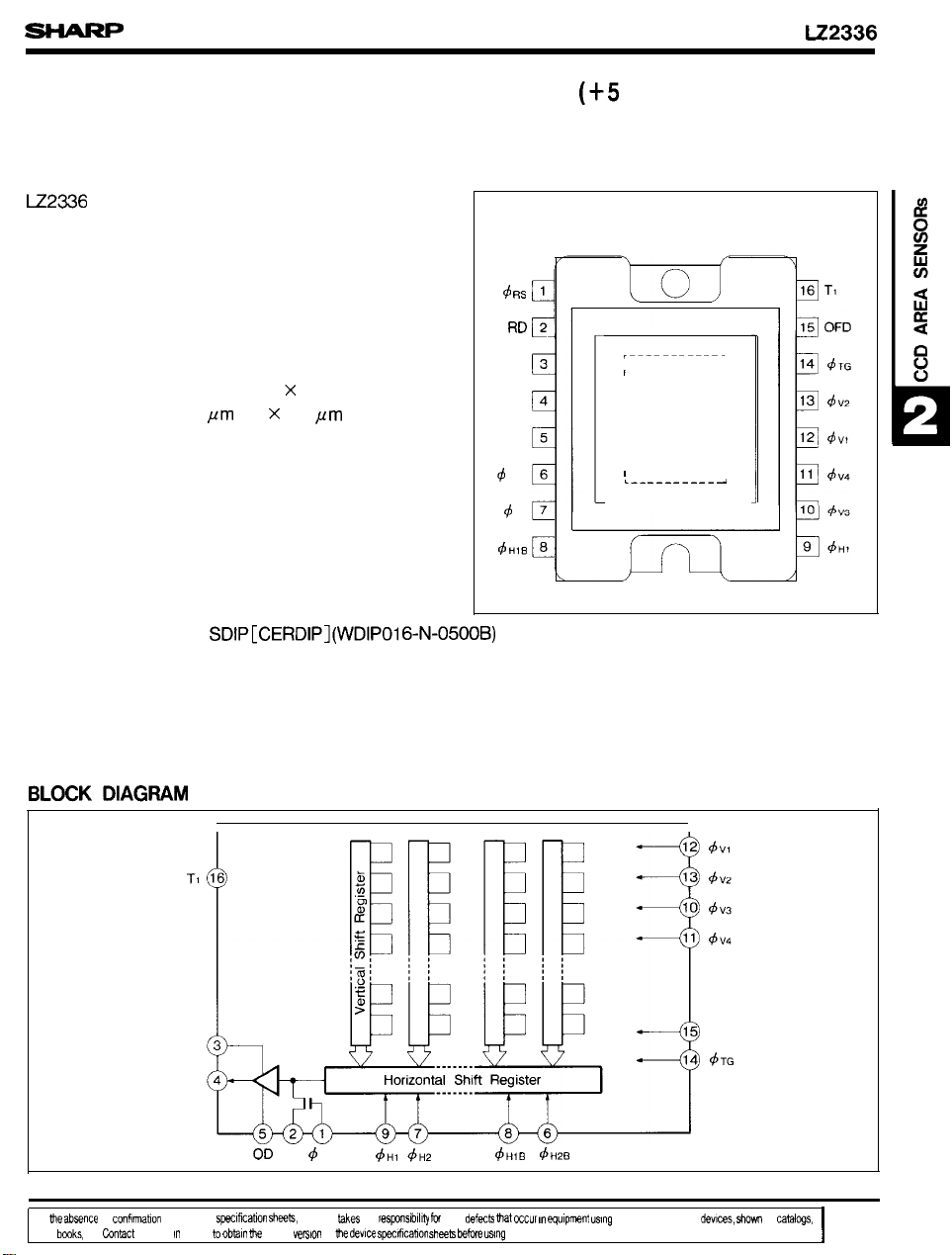
PIN CONNECTIONS
16-PIN SDIP
d
RS
RD
GND
0s
OD
d
H2B
$
H2
dHIB
)
,——_— ——— ——— — ,
,
1
I
.—. ——— ——— ———
J
TOP VIEW
GND
0s
“In
tie
abwnce of conf!mtlon by device swIflcation
dats bwks, etc
hnhct
WARP (n waler to obb[n ti latest
OD
RD d ,S
sh=b,
WARP Wes no reswsib(llv b any defeck hat
@mIon
of
tie dev(ce
dH1 +H2
swdlcabon shwh
dHIB dH2B
bsti us!ng
cccur In
quipmsnt
any SHARPs device
us!ng
OFD
dTG
any of SHARP’s &vIces, zhom In
catalcgs,
I

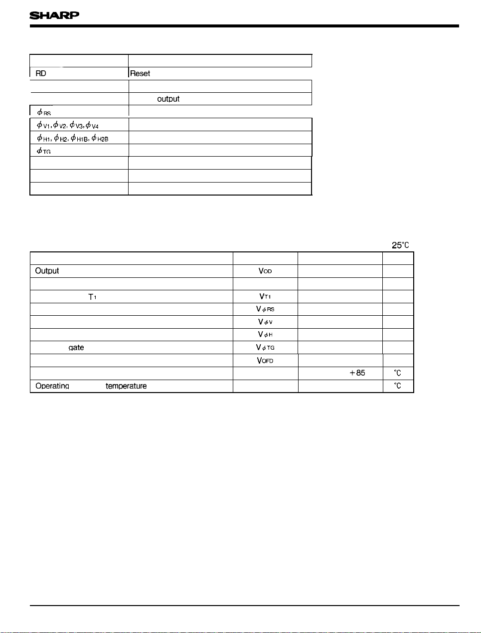
PIN DESCRIPTION
SYMBOL
w-
OD
0s Video
&-
dVl, dV2Yd V3, dV4
4HI,4H2,4H16,4H213
d
TG
OFD
TI Test terminal
GND
I
Reset transistor drain
Output transistor drain
outl)ut
]
Reset transistor gate clock
Vertical shift register gate clock
Horizontal shift register gate clock
Transfer gate clock
Overflow drain
Ground
LZ2336
PIN NAME
I
I
ABSOLUTE MAXIMUM RATINGS
PARAMETER
Out~ut
transistor drain voltage
Reset transistor drain voltage
Test terminal,
Reset sate clock voltage
Vertical shift register clock voltage
Horizontal shift register clock voltage
Transfer qate clock voltage
Overflow drain voltage Vom O to +27 v
Storage temperature
ODeratina
TI
ambient
tem~rature
SYMBOL
VOD
RD
V
VT1
vdRs
Vdv
V4H
VdTG
Tstg
Topr
RATING
Oto +15 v
Oto +15
Oto +15 v
–0.3 to +15 v
–0.3 to +15 v
–0.3 to +15 v
–0.3 to +15 v
–40 to
–20 to +70
(Ta =
+85
2SC
UNIT
v
‘c
‘c
)
150

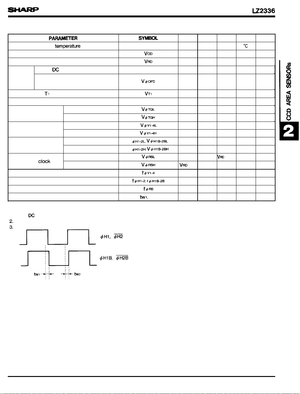
RECOMMENDED OPERATING CONDITIONS
PARAMHER
Operating ambient
Output transistor drain voltage
Reset transistor drain voltage
Overflow
drain
voltage
Test terminal, TI
Ground voltage
Transfer gate clock
Vertical shift
register clock
Horizontal shift
register clock
Reset gate
Vertical shift register clock frequency
Horizontal shift register clock frequency
Reset gate clock frequency
Horizontal shift register clock phase
tem~rature
When N is applied
When pulse is applied
p-p level
LOW level
HIGH level
LOW level
HIGH level
LOW level
HIGH level
clink
LOW level
HIGH level
V
v
SYMSOL
Topr 25.0 ‘c
Vm 12.0
VRO
Vom 3,0
V40M
VT1
GND
V
4TGL
V
4TGH
V4v14L
V4v1-4H
4H1-2L,
V+
HIB-2BL
4H1-2H, VdHIB-ZBH
v4m
v4R2n
f+v14
f+ Hi-2,
f+
H1E2B
f+m
twl, tw2
MIN.
12.0
TYP. MAX.
12.5 14.0
Voo
12.5
VOD
0.0
–0.05
12.0
–
0,05
4.7
– 0.05
4.7
0.0
VRO
0.0 5.0
0.0
12.5 14.0
0.0
5.0
0,0 0.05
5.0 6.0
Vm - 10,5
-6.0 9.5 v
15.73 kHz
6.75
6.75 MHz
12.0
14.0
0,05
0.05
6.0
10.0
UNIT
v
v
v
v
v
v
v
v
v
v
v
v
v
MHz
ns
LZ2336
NOTE
1
2
3
[
fi
@
j
a
8
u
~
L
NOTES :
1. When DC voltage is applied, shutter speed is 1/@ seconds.
2.
When pulse is applied, shutter speed is less than 1/60 seconds.
3“
n_rL
~
:,
::
,,
‘Hi”
‘H”
“
151
 Loading...