

Sharp LZ0P3646, LZ0P3645, LZ0P3642, LZ0P3641 Datasheet
In the absence of confirmation by device specification sheets, SHARP takes no responsibility for any defects that may occur in equipment using any SHARP devices shown in
catalogs, data books, etc. Contact SHARP in order to obtain the latest device specification sheets before using any SHARP device.
1
DESCRIPTION
The LZ0P3641/42∫/45∫/46 are 1/4-type (4.5 mm)
350 000-pixel built-in lens color CCD (chargecoupled device) area sensors. All pixel signals can
be read independently via the vertical shift register
and horizontal shift register. With their small lens
and WLCC-type flat package, it is possible to make
ultra small color camera easily.
FEATURES
• Progressive scan
• Square pixel
• Compatible with VGA format
• Number of effective pixels : 659 (H) x 494 (V)
• Number of optical black pixels
– Horizontal : 2 front and 31 rear
– Vertical : 8 front and 2 rear
• Number of dummy bits
– Horizontal : 16
– Vertical : 5
• Pixel pitch : 5.6 µm (H) x 5.6 µm (V)
• R, G and B primary color mosaic filters
• Low fixed-pattern noise and lag
• Blooming suppression structure
• Built-in output amplifier
• Built-in overflow drain voltage circuit and reset
gate voltage circuit
• Horizontal shift register clock and reset gate clock
voltage : 3.3 V (TYP.)
• Variable electronic shutter (1/30 to 1/10 000 s)
• Built-in optical low-pass-filter
• Integrated lens :
Horizontal viewing angle
LZ0P3641/46 : 50˚
∫LZ0P3642 : 62˚
∫LZ0P3645 : 115˚
• Package
– 14-pin half-pitch WLCC
*
type
– Base section size : 12 mm (H) x 11 mm (V)
–
Outline dimensions (MAX.) : 18 mm (H) x 11 mm (V)
• Package height : approx. 13 mm (two pcs. of lenses)
* Window Leadless Chip Carrier
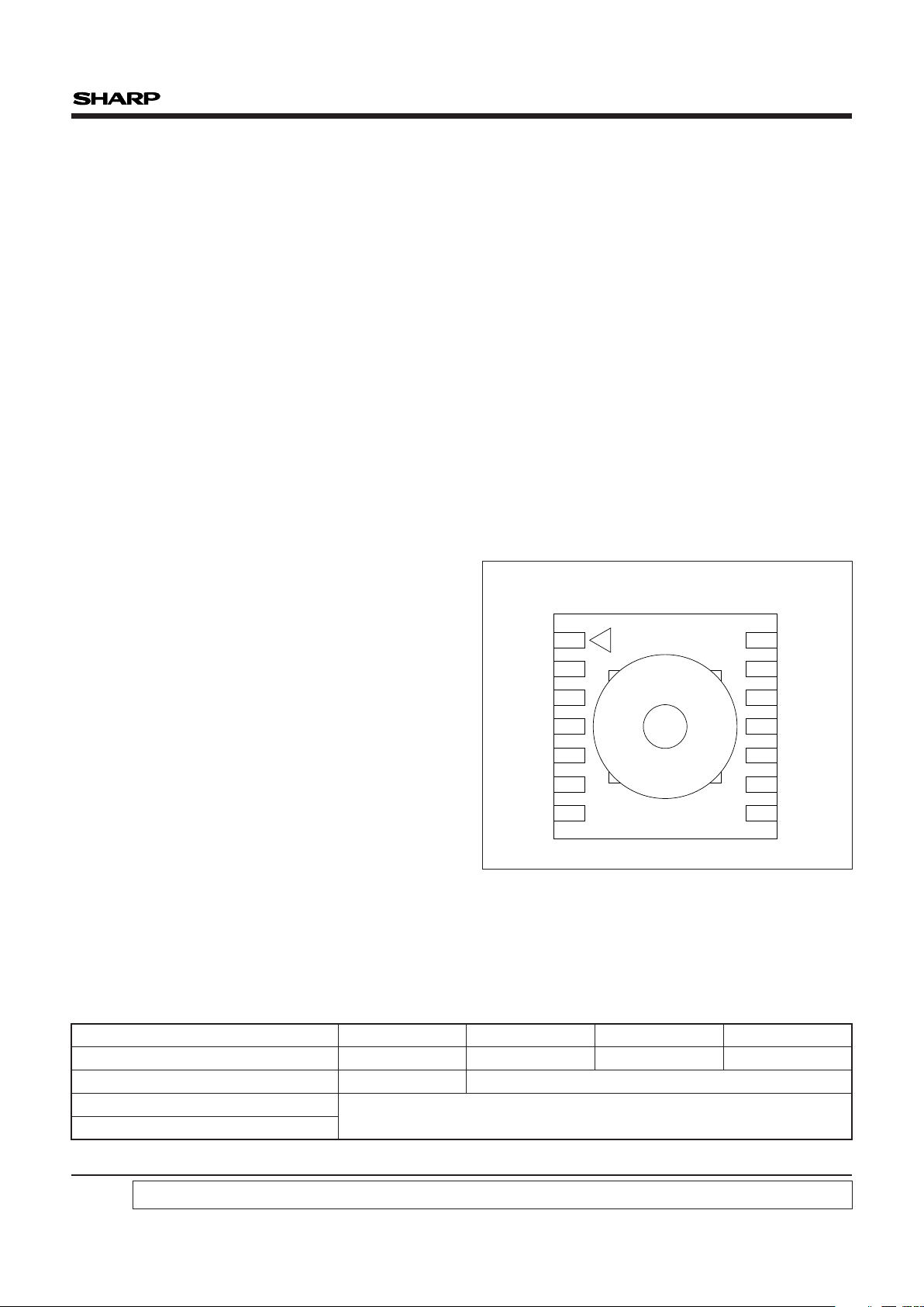
PIN CONNECTIONS
LZ0P3641/3642/3645/3646
LZ0P3641/3642∫/
3645
∫
/3646
1/4-type Built-in Lens Color CCD
Area Sensors with 350 k Pixels
∫Under development
ØV2
Ø
V1
Ø
V3A
Ø
V3B
PW
GND
OS
1
2
3
4
5
6
7
14
13
12
11
10
9
8
Ø
H2
Ø
H1
Ø
RS
NC
OFD
GND
OD
14-PIN HALF-PITCH WLCC TYPE
TOP VIEW
COMPARISON TABLE
Horizontal viewing angle
Lens specification
Characteristics
∫LZ0P3645∫LZ0P3642LZ0P3641
115˚62˚50˚
Refer to each following specification.
50˚
LZ0P3646
3.4 2.8F no.
2
LZ0P3641/3642/3645/3646
PIN DESCRIPTION
ABSOLUTE MAXIMUM RATINGS
(TA = +25 ˚C)
SYMBOL PIN NAME
OD Output transistor drain
OS Output signals
ØRS Reset transistor clock
Ø
V1, ØV2, ØV3A, ØV3B Vertical shift register clock
ØH1, ØH2 Horizontal shift register clock
OFD Overflow drain
PW P-well
GND Ground
NC No connection
PARAMETER SYMBOL RATING UNIT
Output transistor drain voltage V
OD 0 to +18 V
Overflow drain voltage V
OFD Internal output V
Reset gate clock voltage VØRS Internal output V
Vertical shift register clock voltage V
ØV –11.5 to +17.5 V
Horizontal shift register clock voltage VØH –0.3 to +12 V
Voltage difference between P-well and vertical clock V
PW-VØV –29 to 0 V
Voltage difference between vertical clocks V
ØV-VØV 0 to +15 V
–20 to +70 ˚CStorage temperature TSTG
–10 to +60 ˚CAmbient operating temperature TOPR
3
2
1
NOTE
NOTES :
1. Do not connect to DC voltage directly. When OFD is connected to GND, connect VOD to GND. Overflow drain clock is
applied below 27 Vp-p.
2. Do not connect to DC voltage directly. When Ø
RS is connected to GND, connect VOD to GND. Reset gate clock is
applied below 8 Vp-p.
3. When clock width is below 10 µs, and clock duty factor is below 0.1%, voltage difference between vertical clocks will be
below 28 V.
3
LZ0P3641/3642/3645/3646
RECOMMENDED OPERATING CONDITIONS
PARAMETER SYMBOL MIN. TYP. MAX. UNIT NOTE
Ambient operating temperature T
OPR 25.0 ˚C
Output transistor drain voltage V
OD 14.55 15.0 15.45 V
Overflow drain clock
p-p level V1VØOFD 22.5
Ground GND 0.0 V
P-well voltage V
PW –10.0 VØVL V2
Vertical shift
register clock
LOW level
V
ØV1L, VØV2L
VØV3AL, VØV3BL
–9.5 –9.0 –8.5 V
INTERMEDIATE level
V
ØV1I, VØV2I
VØV3AI, VØV3BI
0.0 V
HIGH level V
ØV3AH, VØV3BH 14.55 15.0 15.45 V
Horizontal shift
register clock
LOW level V
ØH1L, VØH2L –0.05 0.0 0.05 V
HIGH level VØH1H, VØH2H 3.0 3.3 5.5 V
Reset gate clock p-p level V
ØRS V1
Vertical shift register clock frequency
f
ØV1, fØV2
fØV3A, fØV3B
15.73 kHz
Horizontal shift register clock frequency f
ØH1, fØH2 12.27 MHz
Reset gate clock frequency fØRS 12.27 MHz
NOTES :
1. Use the circuit parameter indicated in "SYSTEM CONFIGURATION EXAMPLE", and do not connect to DC voltage directly.
2. V
PW is set below VØVL that is low level of vertical shift register clock, or is used with the same power supply that is connected
to V
L of V driver IC.
* To apply power, first connect GND and then turn on V
OD. After turning on VOD, turn on PW first and then turn on other powers
and pulses. Do not connect the device to or disconnect it from the plug socket while power is being applied.
3.0 3.3 5.5
4
LZ0P3641/3642/3645/3646
CHARACTERISTICS FOR LZ0P3641 (1/30 s progressive scan readout mode)
(
TA: +25 ˚C, Operating conditions : The typical values specified in
"RECOMMENDED OPERATING CONDITIONS"
.
Color temperature of light source : 3 200 K)
PARAMETER SYMBOL
Standard output voltage V
O
Saturation output voltage V
SAT
450
MIN. TYP.
150
230150RSensitivity (Green channel) 3
2
1
NOTE
mV
mV
mV
UNITMAX.
8.0 mAOutput transistor drain current I
OD
4.0
%6Shading 45 60
TV line 4Resolution (at center) 250 300
200150Resolution (at corner) 5TV line
Difference of center position 7%±10
NOTES :
1. The average output voltage of G signal in the central
area (H/10, V/10) under uniform illumination.
The standard exposure conditions are defined as when
V
O is 150 mV.
2. The average output voltage of G signal in the central
area (H/10, V/10) under 10 times exposure of the
standard exposure conditions.
3. The average output voltage of G signal in the central
area (H/10, V/10) when a 1 000 lux light source with a
white board of 90% reflector is imaged.
4. The resolution in the central area (H/10, V/10) at which
the image of the TV resolution chart (ex. EIAJ test chart)
can be distinguished on the B/W video monitor when
converted into composite video signals.
5. The resolution in the peripheral area (image height : Y =
0.8) under the conditions mentioned above.
6. Defined by the following formula at the brightness of
standard output voltage : (Vco/Vce) x 100 [%]
Vco : Output voltage at edge of the image (at NTSC
video output).
Vce : Output voltage at center of the image (at NTSC
video output).
7. The difference between the center position of image and
that of the monitor. This is the ratio for the horizontal
underscanning monitor size which includes the decentering
eccentricity when turning the lens head one time.
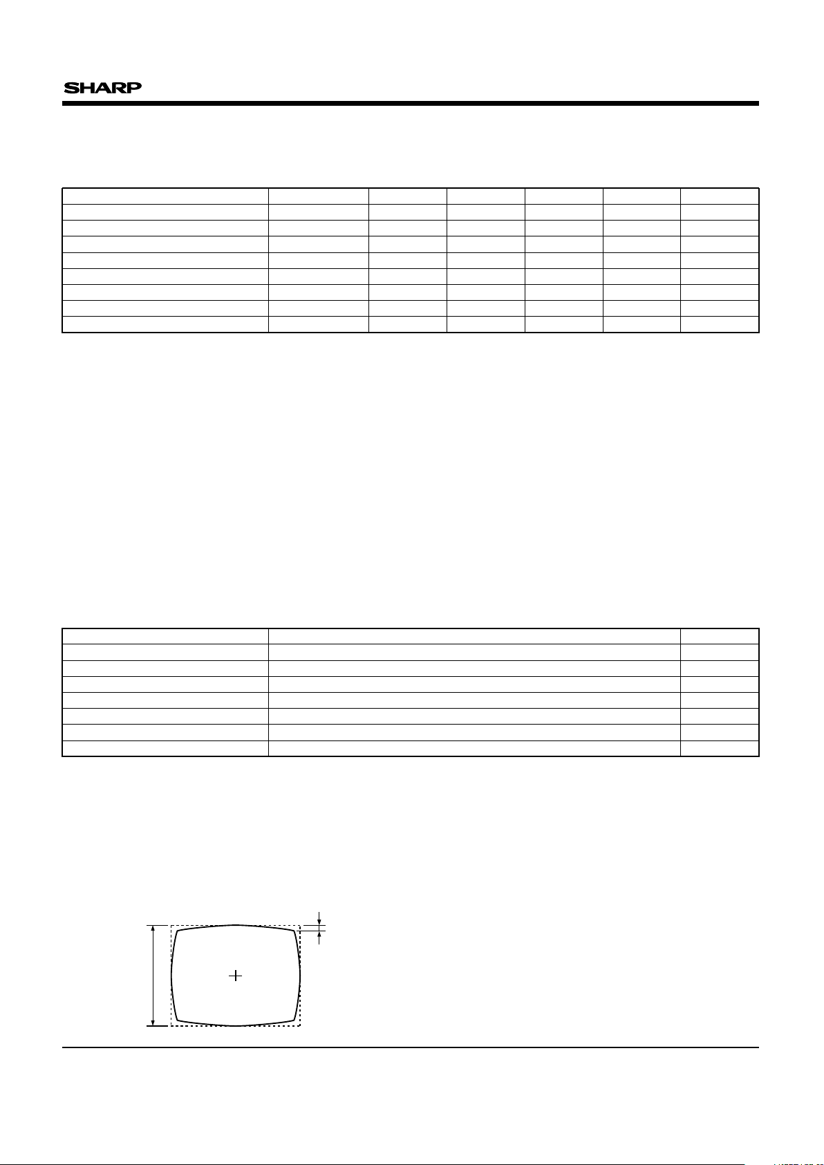
LENS SPECIFICATION FOR LZ0P3641
PARAMETER SPECIFICATION
Construction 2 pcs. (non-spherical, plastic)
Focal length 3.9 mm [TYP. : reference]
NOTE
3.4±5%F No.
Focus adjustment range ∞ to 10 cm 2
TV distortion ≤ –1.0% 1
Viewing angle H : 50˚, V : 38˚, Diagonal : 60˚ [TYP. : reference]
NOTES :
1. TV distortion is defined by the formula, (∆y/y) x 100 [%]
at capturing rectangular pattern sized horizontal by
vertical as 4 by 3.
"y" is defined as the vertical height of the center of the
horizontal line.
∆y is defined as the difference between the vertical height
of the center of the horizontal line and an edge of it.
2. The best focus point of an object can be obtained by
turning the lens head within this range.
3. Torques which are necessary for turning the lens.
* Be careful not to remove the lens head by turning it
counterclockwise too much when adjusting macro.
y
∆y
30.00005 to 0.001 N·mTorque of focusing
 Loading...