

Symbol MIN TYP MAX Unit
V
CC
VLED
ICC
VIH
VIL
IIH
*3
IIL
*4
fCLK
fFR
4.75
(5.75)
------
3.5
------
------
------
-----70
V
mA
V
V
µA
mA
MH
Z
HZ
5.25
(6.25)
260
------
1.5
0.1
0.12
10
1000
5.0
(6.0)
200
------
------
------
------
-----250
*1 Red, *2 Yellow-green,Blue, *3 V
IH=5, *4 VIL=0V
(Ta=25˚C,VCC=5V,V(R, G)=5V,V(B)=8V)
Supply voltage for IC
Supply voltage for LED
IC current dissipation
Input voltage
Input current
Clock frequency
Frame frequency
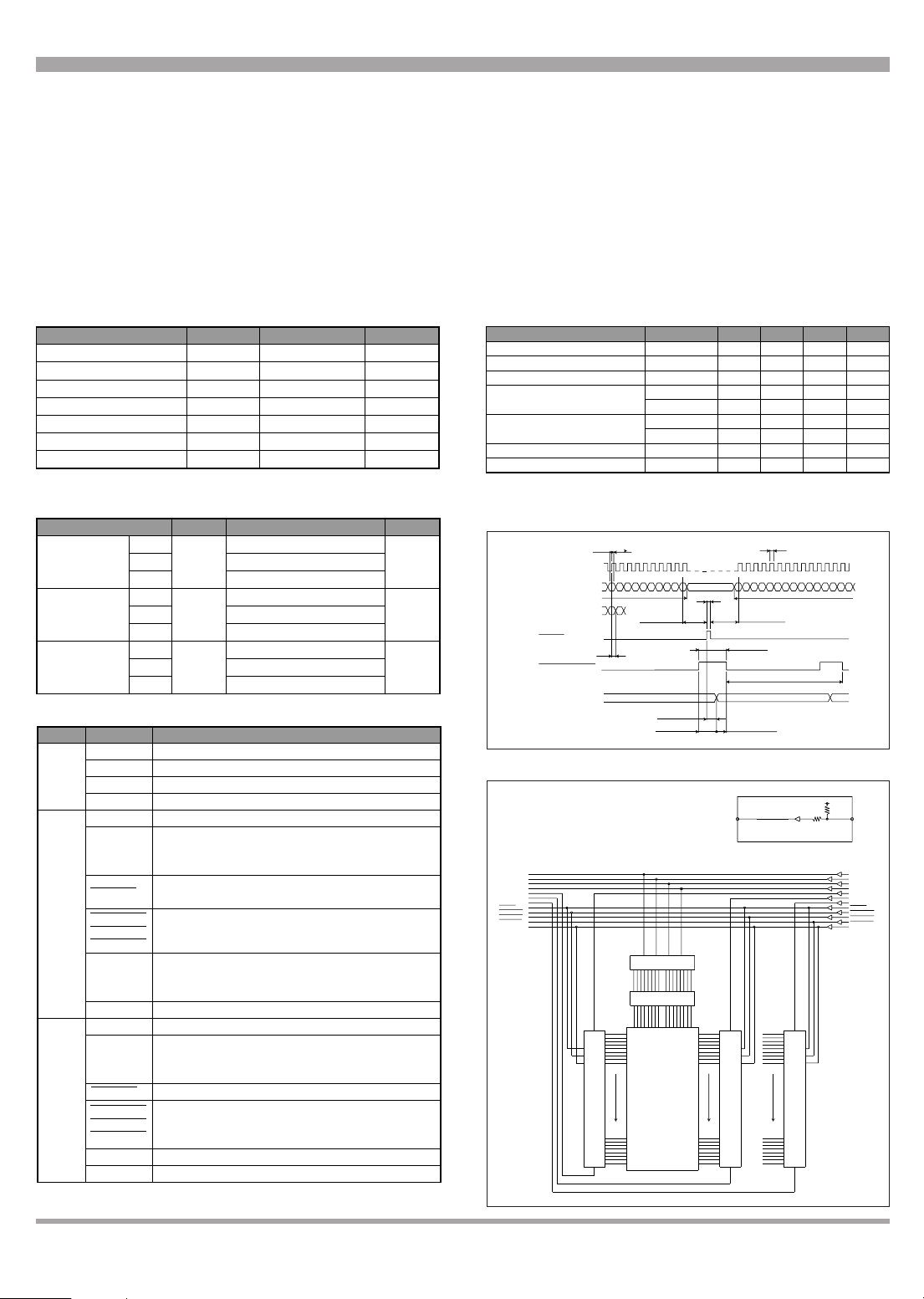
Parameter
VD(n+1)data on
VD(n+2) data
tWCLK
OFF
V
D(n+1)
1/f ENA
tWENA
td(L-C)
td(A-E)
R, G, B
DATA
CLOCK
V
D(n+1) data
thtsu
ADDRESS
(A0 to A3)
td(L-A)
td(E-A)
VD(n)data on
R, G, B
DATA(OUT)
R, G, B ENABLE
V
D(n)
LATCH
t
dD
td(C-L)
tWL
1
473
331
CLOCK
A0
A1
A2
A3
RDATA
GENABLE
BENABLE
IN
GDATA
BDATA
LATCH
RENABLE
GDATA
Nch FET DRIVER
FOR BLUE
A0
A1
BDATA
LATCH
RENABLE
GENABLE
BENABLE
CLOCK
OUT
A2
A3
RDATA
FOR YELLOW-GREEN
FOR RED
LED MATRIX
16✕16DOT✕2
32BIT
AND LUMINANCE ADJUSTMENT CIRCUIT
SHIFT-REGISTER, LATCH, DRIVER
SHIFT-REGISTER, LATCH, DRIVER
AND LUMINANCE ADJUSTMENT CIRCUIT
HC367
I/O part
4 TO 16 DECODER
AND LUMINANCE ADJUSTMENT CIRCUIT
32BIT
SHIFT-REGISTER, LATCH, DRIVER
32BIT
TRICHROMATIC
Full Color Dot Matrix LED Unit for Indoor Use LT1550W(Chip Type)
Unit
V
CC
VLED
V1
tON
Topr
Tstg
P
V
V
V
ms
˚C
˚C
W
(Ta=25˚C)
Supply voltage for IC
Supply voltage for LED
Input voltage
Turn-on time
Operating temperature
Storage temperature
Power dissipation
Parameter
Symbol
-0.3 to +5.5
-0.3 to (+6.5)
-0.3 to V
CC+0.3
1
-10 to +60
-20 to +70
62
Rating
Red
Yellow-green
Blue
Red
Yellow-green
Blue
Red
Yellow-green
Blue
(100)
(150)
(70)
635
565
430
35
30
65
Luminance
Peak emission wavelength
Spectrum radiation bandwidth
cd/m
2
nm
nm
L
V
λp
∆λ
Parameter Symbol UnitTYP.
(Ta=25˚C,VCC=5V,V(R, G)=5V,V(B)=8V)
Supply voltage for LED(Red,Yellow-green)+5V
Supply voltage for LED(Blue)+(+8V±10%)
Supply voltage for IC+5V
Ground
Address specification signal for row driver
Serial data input for each color(H:ON, L:OFF)
Latch signal of display data(H: Serial data is converted
to parallel data.L: Contents are latched.)
Controls ON/OFF of each color of LED
(H: LED OFF)
Clock signal for data transmission in the shiftregister.(L/H: serial data is shifted.)
Ground for signal
Buffered input signal
Input signal generated through 32-bit shift
register
Buffered input signal
Buffered input signal
Buffered input signal
Ground for signal
Symbol Function
V
(R,G)
V(B)
VCC
GND
A0 to A3
LATCH
CLOCK
GND
A0 to A3
RDATA
GDATA
BDATA
RDATA
GDATA
BDATA
LATCH
CLOCK
GND
RENABLE
GENABLE
BENABLE
RENABLE
GENABLE
BENABLE
Each signal is used as input signal for next unit.
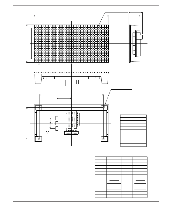
* As for the terminal number, refer to the outline dimensions.
Connector
Power
supply
(CN1)
Input
signal
(CN2)
Output
signal
(CN3)
(Under development)
■ Features
¡No. of dots : 16✕32dots
¡Outline dimensions : 64✕128mm
¡Dot size : 3.0✕3.0mm
¡Dot pitch : 4.0mm
¡Radiation color : Blue+Yellow-green+Red(Full color)
¡Driving method : 1/16 duty dynamic drive
■ Absolute Maximum Ratings ■ Electrical Characteristics
■ Optical Characteristics
■ Terminal Functions
■ Timing Chart
■ Block Diagram
(Notice) ¡
(Internet) ¡Data for sharp's optoelectronic/power device is provided for internet.(Address http://www.sharp.co.jp/ecg/)
In the absence of confirmation by device specification sheets, SHARP takes no responsibility for any defects that may occur in equipment using any SHARP
devices shown in catalogs, data books, etc. Contact SHARP in order to obtain the latest device specification sheets before using any SHARP device.
24
20
VD31
128
4-M3
HD0
-0.5
+0
110
(25)
HD15
6
No.
1
GND
GND
GND
GND
Name
GND
A0
No.
5
4
3
2
1 V(B)
V(B)
V(R,G)
V(R,G)
VCC
Name
CN2
No.
1 A0
8
9
10
7
3
2
10
LATCH
BDATA
A2
A1
A3
RDATA
GDATA
210A1
A2
A3
11
6
7
9
8
5
1312GND
CLOCK
11
9
8
7
6
5
4
13
12
4
3
13
CN2(IN)
CN1
1
1
13
10
CN3
(OUT)
VR1
VR3
VR2
1
54
(9) (9)
-0.5
+0
512-❏3(LED)
RENABL
GENABL
CN3
(Power supply)
CN1
VD0
Data shift direction
BENABL
(Depth Min. 6)
(Input signal) (Output signal)
Name
GND
CLOCK
LATCH
BDATA
BENABLE
RENABLE
GENABLE
RDATA
GDATA
64
Pin connection
15
6
No.
1
GND
GND
GND
GND
Name
GND
A0
No.
5
4
3
2
1 V(B)
V(B)
V(R,G)
V(R,G)
VCC
Name
CN2
No.
1 A0
8
9
10
7
3
2
10
LATCH
BDATA
A2
A1
A3
RDATA
GDATA
210A1
A2
A3
11
6
7
9
8
5
1312GND
CLOCK
11
9
8
7
6
5
4
13
12
4
3
RENABL
GENABL
CN3
(Power supply)
CN1
BENABL
(Input signal) (Output signal)
Name
GND
CLOCK
LATCH
BDATA
BENABLE
RENABLE
GENABLE
RDATA
GDATA
VD31
192
H
D0
-0.5
+0
HD15
-0.5
+0
512-❏3 chipLED
VD0
Data shift direction
96
13.2
8.2
Pin connection
VR3(B)
V
R2(GREEN)
V
R1(RED)
CN1
1 1
10
13
(15)
76 76
8-N3
20
84
(10)(10)
(10)
1
CN2
IN
CN3
CUT
13
LT1550W
 Loading...