

Sharp LT1550ED Datasheet
t
1/ f
td(A-E)
td(L-C)
V
D(n+2) data
tsu th
td(E-A)
td(L-A)
td(C-L)
VD(n+1) data
t
WENA
t
dD
t WL
WCLK
DATA(OUT)
R&G
LATCH
DATA
R&G
CLOCK
ENABLE
V
D(n) data ON
V
D(n)
ADDRESS
V
D(n+1)
(A0 to A3)
OFF
ENA
V
D(n+1) data ON
OFF
Dot Matrix LED Unit for Indoor Use LT1550ED(Chip Type)
Parameter
Supply voltage for IC V
CC -0.3 to +5.5 V
(Ta=25˚C)
*1 25% or less of lighting
Symbol Rating
Unit
VLED -0.3 to +4.5 V
V
1 -0.3 to Vcc+0.3 V
t
ON 1 ms
T
opr -10 to +60
*1
˚C
T
stg -20 to +70 ˚C
P 20 W
Supply voltage for LED
Input voltage
Turn-on time
Operating temperature
Storage temperature
Power dissipation
Parameter
Red
Yellow-green
Red
Yellow-green
120
cd/m
2
Symbol TYP.
Unit
Lv
180
120 ˚
2θ
1
/
2
635
nm
λp
565
Luminance
Viewing angle
Peak emission wavelength
(VCC=5V,VLED=4V,Ta=25˚C)
Connector
V
LED
VCC
Power
supply
(CN1)
Input
signal
(CN2)
Output
signal
(CN3)
GND
A0 to A3
RDATA
GDATA
LATCH
ENABLE
CLOCK
GND
A0 to A3
RDATA
GDATA
LATCH
ENABLE
CLOCK
GND
Supply voltage for LED (+4V)
Supply voltage for IC (+5V)
Ground
Address specification signal for row driver
Serial data input for red (H=ON, L=OFF)
Serial data input for yellow-green (H=ON, L=OFF)
Latch signal of display data. H: Serial data is
converted to parallel data. L: Contents are latched.
Controls ON/OFF of LED (H: LED OFF)
Clock signal for data transmission in the
shift-register. (L→H: serial data is shifted.)
Ground for signal
Buffered input signal
Input signal generated through 32-bit shift register
or buffer
Input signal generated through 32-bit shift register
or buffer
Buffered input signal
Buffered input signal
Buffered input signal
Ground for signal
Symbol Function
Each signal is used as input signal for next unit.
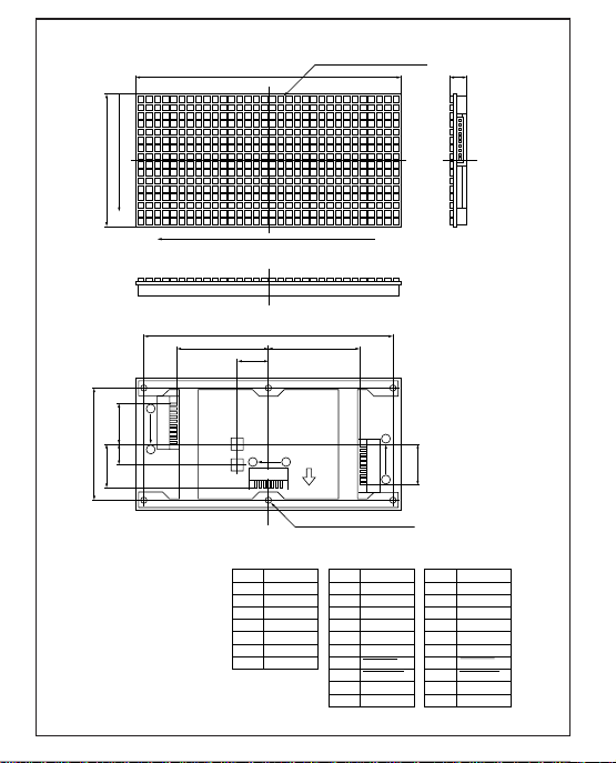
* As for the terminal number, refer to the outline dimensions.
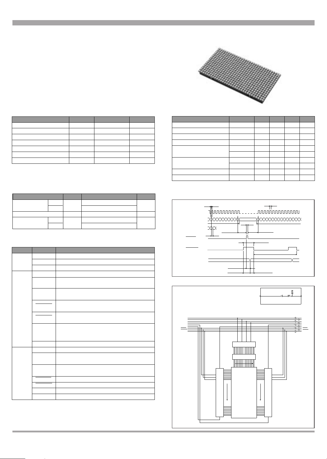
AND LUMINANCE ADJUSTMENT CIRCUIT
AND LUMINANCE ADJUSTMENT CIRCUIT
Pch FET DRIVER
DICHROMATIC
16✕16DOT✕2
LED MATRIX
32BIT
32BIT
Input/output circuit
HC367
331
473
A0
A1
A2
RDATA
GDATA
LATCH
CLOCK
IN
A3
ENABLE
OUT
4 TO 16 DECODER
SHIFT-REGISTER, LATCH, DRIVER
SHIFT-REGISTER, LATCH, DRIVER
A0
A1
A2
RDATA
GDATA
LATCH
CLOCK
A3
ENABLE
■ Features
¡No. of dots : 16✕32dots
¡Outline dimensions : 64.0✕128.0mm
¡Dot size : 3.0✕3.0mm
¡Dot pitch : 4.0mm
¡Radiation color : Yellow-green+Red(dichromatic type)
¡Driving method : 1/16 duty dynamic drive
LT1550ED
■ Absolute Maximum Ratings
■ Optical Characteristics
■ Terminal Functions
■ Electrical Characteristics
Parameter
Supply voltage for IC
Supply voltage for LED
IC current dissipation
LED current dissipation
Input voltage
Input current
Clock frequency
Frame frequency
Symbol MIN. TYP. MAX.
VCC
*1
VLED
ICC
*1
ILED
VIH
VIL
IIH
IIL
fCLK
fFR
(VCC=5V,VLED=4V,Ta=25˚C)
4.75
3.75
------
140
------
3.5
------
------
------
------
------
------
------
------
------
70
250
*1 Under the condition that dichromatic all dots are lit.
■ Timing Chart
■ Block Diagram
5.0
4.0
3.8
5.25
4.25
200
4.2
------
1.5
0.1
0.12
10
1 000
Unit
V
V
mA
A
V
V
µA
mA
MH
HZ
Z
(Notice) ¡
(Internet) ¡Data for sharp's optoelectronic/power device is provided for internet.(Address http://www.sharp.co.jp/ecg/)
In the absence of confirmation by device specification sheets, SHARP takes no responsibility for any defects that may occur in equipment using any SHARP
devices shown in catalogs, data books, etc. Contact SHARP in order to obtain the latest device specification sheets before using any SHARP device.
161
±1
36.0
30.0
CN1
VV12
3
4
HD0
VD15
VD0
±0.2
HD15
(Output signal)
GND1
9
8
3
A
A
A
A
RDATA5
4
3
2
2
CN3
1
0
1
4
3
2
1
0
1
2
3
CN2
A
A
A
A
RDATA
LATCH7
10
CLOCK
LATCH7
9
810ENABLE
CLOCK
GND1
5
6.6
8 MIN
4-M3.0
1
13 MAX
6.6
±0.1
28.0
62.5
25.0
19 MAX
7 MIN
1010
2 MAX
23.2
1
CN3
VR1VR2
CN1
8MAX
28.0
23.5
4.5
28.0
±0.1
10.5
22.8
4
±0.1
4
28.0
1
6
32.0 MAX
6 GDATA GDATA
±0.2
Pin connection
(Power supply)
LED
CC
GND1
GND2
16.5
62.5
CN2
20 MAX
(Input signal)
19 MAX
P4.0✕15=60.0
63.8
P4.0X15=60.0
63.8
(Depth 6.0)
256-ø2.8
±0.1
ENABLE
128
64
8.2
HD0
VD0 VD31
Data shift direction
HD15
44.0 44.0
15.0
1
7
CN3
CN2
10
54
±0.25
22.0
10.0 19.7
1
10
OUT
IN
6-M3
Insert nut
(Effective screw depth 4.0)
19.7
VR1
VR2
1A0
2
3
4
5
6
7
8
9
10
A1
A2
A3
RDATA
GDATA
LATCH
ENABLE
CLOCK
GND
CN2(Input signal)
Pin No.
Name
Pin connection
1A0
2
3
4
5
6
7
8
9
10
A1
A2
A3
RDATA
GDATA
LATCH
ENABLE
CLOCK
GND
Pin No.
Name
CN3(Output signal)
1 VLED
2
3
4
5
6
VLED
VLED
VCC
GND
GND
CN1(Power supply)
Pin No.
Name
7 GND
512-3❏ chip LED
CN1
1
-0.8
+0
-0.5
+0
110
±0.25
4
LT1550ED
 Loading...