

Data Sheet
LRS1341/LRS1342
Stacked Chip
16M Flash Memory and 2M SRAM
FEATURES
• Flash Memory and SRAM
• Stacked Die Chip Scale Package
• 72-ball CSP (FBGA072-P-0811) plastic package
• Power supply: 2.7 V to 3.6 V
• Operating temperature: -25°C to +85°C
•Flash Memory
– Access time (MAX.): 100 ns
– Operating current (MAX.):
The current for F-V
– Read: 25 mA (t
pin
CC
CYCLE
= 200 ns)
– Word write: 17 mA
– Block erase: 17 mA
– Deep power down current (the current for
pin): 10 µA (MAX. F-CE ≥ F-VCC - 0.2 V,
F-V
CC
≤ -0.2 V, F-VPP ≤ 0.2 V)
F-RP
– Optimized array blocking architecture
– Two 4K-word boot blocks
– Six 4K-word parameter blocks
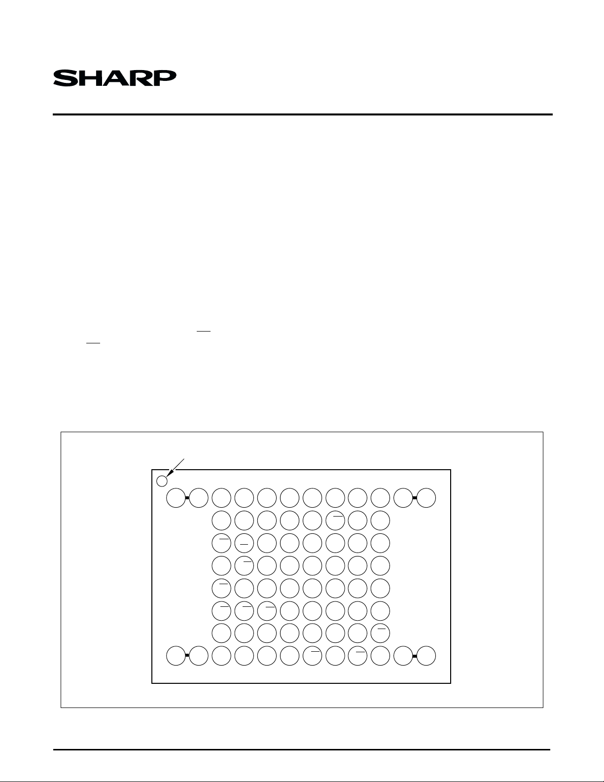
PIN CONFIGURATION
– Thirty-one 32K-word main blocks
– Top/Bottom boot location versions
– Extended cycling capability
– 100,000 block erase cycles
– Enhanced automated suspend options
– Word write suspend to read
– Block erase suspend to word write
– Block erase suspend to read
•SRAM
– Access time (MAX.): 85 ns
– Operating current (MAX.):
– 45 mA
–8 mA (t
, tWC = 1 µs)
RC
– Standby current: 45 µA (MAX.)
– Data retention current: 35 µA (MAX.)
DESCRIPTION
The LRS1341/LRS1342 is a combination memory
organized as 1,048,576 × 16-bit flash memory and
131,072 × 16-bit static RAM in one package.
INDEX
1234567
A
NC NC NC A
B
C
D
E
F
G
NC NC
H NC A5A4A
NOTE: Two NC pins at the corner are connected.
A
16
F-WE
GND
F-WP
S-LB
F-A18F-A17A7A6A3A
Figure 1. LRS1341/LRS1342 Pin Configuration
A11A
15
14
10
T1T
T
2
S-OE
A
9
3
T
4
NC DQ
0
A8A
F-RY/
BY
F-RP
F-VPPF-A19DQ11T
S-UB
A
DQ
DQ
DQ
TOP VIEW72-BALL FBGA
8
910
GND
12
13
DQ
S-WE
15
DQ
13
S-CE
12
DQ
5
DQ
9
GND
14
DQ
6
4
S-V
CC
2
DQ
10
2
DQ
8
0
A
2
1
F-OEF-CE
DQ
DQ
F-V
CC
DQ
DQ
S-CE
11
12
NCNCA
NC
7
5
3
1
1
NCNC
NC
LRS1342-1
Data Sheet 1
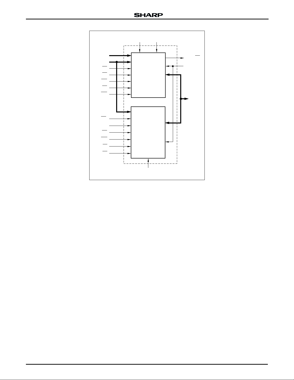
LRS1341/LRS1342 Stacked Chip (16M Flash & 2M SRAM)
CC
F-V
PP
A
F-A
F-A
0
17
19
to A
F-V
to
16
F-CE
F-OE
16M (x16) BIT
FLASH MEMORY
F-WE
F-RP
F-WP
S-CE
1
S-CE
2
S-OE
2M (x16) BIT
SRAM
S-WE
S-LB
S-UB
S-V
CC
Figure 2. LRS1341/LRS1342 Block Diagram
F-RY/BY
GND
DQ0 to
DQ
15
LRS1342-2
2 Data Sheet
Stacked Chip (16M Flash & 2M SRAM) LRS1341/LRS1342
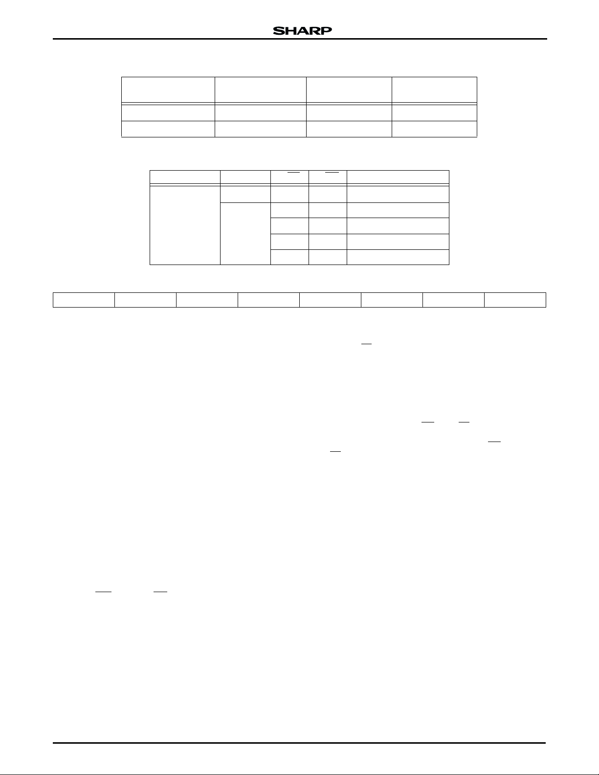
Table 1. Pin Descriptions
PIN DESCRIPTION TYPE
to A
A
0
16
F-A
to F-A
17
F-CE
, S-CE2Chip Enable Inputs (SRAM) Input
S-CE
1
F-WE
S-WE
F-OE
S-OE
S-LB
S-UB
Address Inputs (Common) Input
Address Inputs (Flash) Input
19
Chip Enable Input (Flash) Input
Write Enable Input (Flash) Input
Write Enable Input (SRAM) Input
Output Enable Input (Flash) Input
Output Enable Input (SRAM) Input
SRAM Byte Enable Input (DQ0 to DQ7) Input
SRAM Byte Enable Input (DQ8 to DQ15) Input
Reset/Power Down (Flash)
F-RP
Block erase and Word Write: V
Read: VIH or V
Reset/Power Down: V
HH
IL
IH
or V
HH
Input
Write Protect (Flash)
F-WP
Two Boot Blocks Locked: V
(with F-RP = VHH
IL
Input
Erase of Write can operate to all blocks)
Ready/Busy (Flash)
F-RY/BY
DQ
to DQ
0
F-V
S-V
CC
CC
During an Erase or Write operation: V
Block Erase and Word Write Suspend: HIGH-Z
Deep Power Down: V
Data Input/Outputs (Common) Input/Output
15
OH
Power Supply (Flash) Power
Power Supply (SRAM) Power
OL
Output
Write, Erase Power Supply (Flash)
F-V
PP
Block Erase and Word Write: F-V
All Blocks Locked: F-VPP < V
PPLK
PP
= V
PPLK
Power
GND Ground (Common) Power
NC No Connection —
T
to T
1
5
Test Pins (Should be Open) —
Data Sheet 3
LRS1341/LRS1342 Stacked Chip (16M Flash & 2M SRAM)
Table 2. Truth Table
FLASH SRAM F-CE
Read Standby L H L H
Output Disable Standby L H H H X X HIGH-Z 3
Write Standby L H H L X X D
F-RP F-OE F-WE S-CE1S-CE2S-OE S-WE S-LB S-UB
See Note 4
1
XX
See Note 4
DQ0 DQ-7
DQ8 DQ
15
D
OUT
IN
2, 3, 5, 6
Read H H X X L H L H See Note 7
Standby
Reset/Power Down
Output
Disable
Write H H X X L H L L
Read X L X X L H L H
Output
Disable
H H X X L H H H X X HIGH-Z
H H X X L H X X H H HIGH-Z
See Note 7
XLX X L H HH XX HIGH-Z
X L X X L H X X H H HIGH-Z
Write X L X X L H L L See Note 7
Standby Standby H H X X
Reset/Power Down Standby X L X X X X HIGH-Z 3
NOTES:
1. L = V
2. Refer to the ‘Flash Memory Command Definition’ section for valid
3. F-WP
, H = VIH, X = H or L. Refer to DC Characteristics.
IL
during a write operation.
D
IN
set to VIL or VIH.
4. SRAM standby mode. See Table 2a.
See Note 4
5. Command writes involving block erase or word write are reliably
6. Never hold F-OE
7. S-LB
XX
executed when F-V
erase or word write with V
See Note 4
= V
PP
PPH
< RP < VHH produce spurious results
IH
and should not be attempted.
LOW and F-WE LOW at the same time.
, S-UB control mode. See Table 2b.
HIGH-Z 3
and F-VCC = 2.7 V to 3.6 V. Block
NOTES
2, 3
MODE
Standby
(SRAM)
COMMAND
Table 2a.
PINS
S-CE
S-CE
1
S-LB S-UB
2
HXXX
XLXX
XXHH
Table 3. Command Definition for Flash Memory
BUS CYCLES
REQUIRED
OPERATION
FIRST BUS CYCLE SECOND BUS CYCLE
2
ADDRESS
3
MODE
(SRAM)
Read/Write
3
DATA
S-LB
LLD
LHD
HLHIGH-ZD
OPERATION2ADDRESS3DATA
Table 2b.
PINS
S-UB DQ0 - DQ7DQ8 - DQ
OUT/DIN
OUT/DIN
1
3
D
OUT/DIN
HIGH-Z
OUT/DIN
NOTES
Read Array/Reset 1 Write XA FFH
Read Identifier Codes ≥ 2 Write XA 90H Read IA ID 4
Read Status Register 2 Write XA 70H Read XA SRD
Clear Status Register 1 Write XA 50H
Block Erase 2 Write BA 20H Write BA D0H 5
Word Write 2 Write WA 40H or 10H Write WA WD 5
Block Erase and Word
Write Suspend
Block Erase and Word
Write Resume
NOTES:
1. Commands other than those shown in table are reserved by
SHARP for future device implementations and should not be used.
2. BUS operations are defined in Table 2.
3. XA = Any valid address within the device;
IA = Identifier code address;
BA = Address within the block being erased;
1WriteXAB0H 5
1WriteXAD0H 5
WA = Address of memory location to be written;
SRD = Data read from status register, see Table 6;
WD = Data to be written at location WA. Data is latched on the
rising edge of F-WE
or F-CE (whichever goes high first);
ID = Data read from identifier codes.
4. See Table 4 for Identifier Codes.
5. See Table 5 for Write Protection Alternatives.
15
4 Data Sheet
Stacked Chip (16M Flash & 2M SRAM) LRS1341/LRS1342
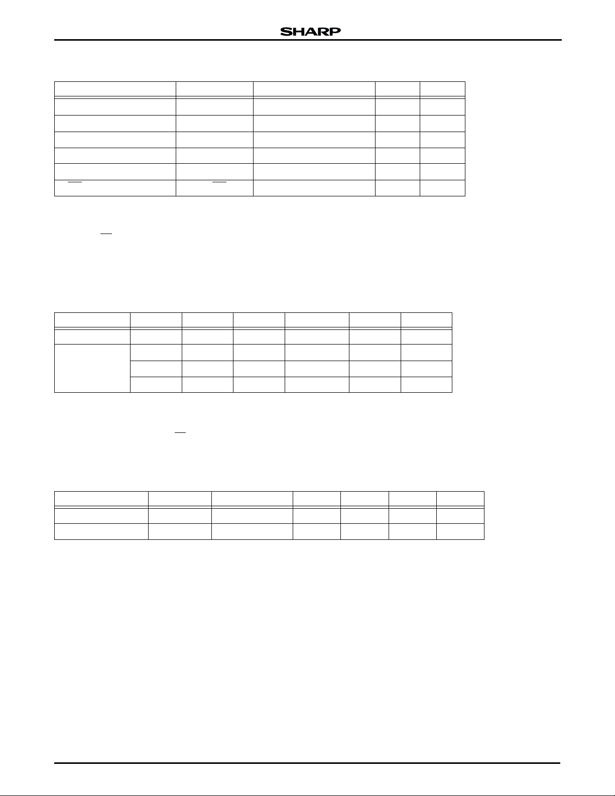
Table 4. Identifier Codes
CODES
ADDRESS
- A18)
(A
0
LRS1341 DATA
(DQ0 - DQ7)
LRS1342 DATA
(DQ0 - DQ7)
Manufacture Code 00000H B0H B0H
Device Code 00001H 48H 49H
Table 5. Write Protection Alternatives
OPERATION F-V
Block Erase or
Word Write
> V
V
IL
PPLK
PP
F-RP F-WP EFFECT
XX
V
IL
V
HH
V
IH
V
IH
V
All blocks locked
All blocks locked
X
All blocks unlocked
X
Two boot blocks locked
V
IL
All blocks unlocked
IH
Table 6. Status Register Definition
WSMS ESS ES WWS VPPS WWSS DPS R
76543210
SR.7 = Write State Machine Status (WSMS)
1 = Ready
0 = Busy
SR.6 = Erase Suspend Status (ESS)
1 = Block Erase Suspended
0 = Block Erase in Progress/Completed
SR.5 = Erase Status (ES)
1 = Error in Block Erasure
0 = Successful Block Erase
SR.4 = Word Write Status (WWS)
1 = Error in Word Write
NOTES:
1. Check RY/BY
completion. SR.6 - SR.0 are invalid while SR.7 = 0.
2. If both SR.5 and SR.4 are ‘1’s after a block erase attempt, an
improper command sequence was entered.
3. SR.3 does not provide a continuous indication of F-V
WSM interrogates and indicates the F-V
Erase or Word Write command sequences. SR.3 is not guaranteed
to report accurate feedback only when F-V
4. The WSM interrogates the F-WP
or Word Write command sequences. It informs the system,
depending on the attempted operation, if the F-WP
F-RP
5. SR.0 is reserved for future use and should be masked out when
is not VHH.
polling the status register.
or SR.7 to determine block erase or word write
≠ V
PP
, V
PPH1
is not VIH or
level only after Block
PP
and F-RP only after Block Erase
PP
0 = Successful Word Write
level. The
.
PPH2
SR.3 = V
1 = F-V
0 = F-V
Status (VPPS)
PP
LOW Detect, Operation Abort
PP
Okay
PP
SR.2 = Word Write Suspend Status (WWSS)
1 = Word Write Suspended
0 = Word Write in Progress/Completed
SR.1 = Device Protect Status (DPS)
1 = F-WP
and/or F-RP Lock Detected,
Operation Abort
0 = Unlock
SR.0 = Reserved for future enhancements (R)
Data Sheet 5
LRS1341/LRS1342 Stacked Chip (16M Flash & 2M SRAM)
MEMORY MAPS
[A0 - A19]
FFFFF
F8000
F7FFF
F0000
EFFFF
E8000
E7FFF
E0000
DFFFF
D8000
D7FFF
D0000
CFFFF
C8000
C7FFF
C0000
BFFFF
B8000
B7FFF
B0000
AFFFF
A8000
A7FFF
A0000
9FFFF
98000
97FFF
90000
8FFFF
88000
87FFF
80000
7FFFF
78000
77FFF
70000
6FFFF
68000
67FFF
60000
5FFFF
58000
57FFF
50000
4FFFF
48000
47FFF
40000
3FFFF
38000
37FFF
30000
2FFFF
28000
27FFF
20000
1FFFF
18000
17FFF
10000
0FFFF
08000
07FFF
07000
06FFF
06000
05FFF
05000
04FFF
04000
03FFF
03000
02FFF
02000
01FFF
01000
00FFF
00000
32K-WORD MAIN BLOCK
32K-WORD MAIN BLOCK
32K-WORD MAIN BLOCK
32K-WORD MAIN BLOCK
32K-WORD MAIN BLOCK
32K-WORD MAIN BLOCK
32K-WORD MAIN BLOCK
32K-WORD MAIN BLOCK
32K-WORD MAIN BLOCK
32K-WORD MAIN BLOCK
32K-WORD MAIN BLOCK
32K-WORD MAIN BLOCK
32K-WORD MAIN BLOCK
32K-WORD MAIN BLOCK
32K-WORD MAIN BLOCK
32K-WORD MAIN BLOCK
32K-WORD MAIN BLOCK
4K-WORD PARAMETER BOOT BLOCK
4K-WORD PARAMETER BOOT BLOCK
4K-WORD PARAMETER BOOT BLOCK
4K-WORD PARAMETER BOOT BLOCK
4K-WORD PARAMETER BOOT BLOCK
4K-WORD PARAMETER BOOT BLOCK
4K-WORD BOOT BLOCK
4K-WORD BOOT BLOCK
30
2932K-WORD MAIN BLOCK
2832K-WORD MAIN BLOCK
2732K-WORD MAIN BLOCK
2632K-WORD MAIN BLOCK
2532K-WORD MAIN BLOCK
2432K-WORD MAIN BLOCK
2332K-WORD MAIN BLOCK
2232K-WORD MAIN BLOCK
2132K-WORD MAIN BLOCK
2032K-WORD MAIN BLOCK
1932K-WORD MAIN BLOCK
18 32K-WORD MAIN BLOCK
1732K-WORD MAIN BLOCK
1632K-WORD MAIN BLOCK
15
14
13
12
11
10
9
8
7
6
5
4
3
2
1
0
5
4
3
2
1
0
1
0
BOTTOM BOOT
LRS1342-3
Figure 3. Bottom Boot for Flash Memory
[A0 - A19]
FFFFF
F8000
F7FFF
F0000
EFFFF
E8000
E7FFF
E0000
DFFFF
D8000
D7FFF
D0000
CFFFF
C8000
C7FFF
C0000
BFFFF
B8000
B7FFF
B0000
AFFFF
A8000
A7FFF
A0000
9FFFF
98000
97FFF
90000
8FFFF
88000
87FFF
80000
7FFFF
78000
77FFF
70000
6FFFF
68000
67FFF
60000
5FFFF
58000
57FFF
50000
4FFFF
48000
47FFF
40000
3FFFF
38000
37FFF
30000
2FFFF
28000
27FFF
20000
1FFFF
18000
17FFF
10000
0FFFF
08000
07FFF
07000
06FFF
06000
05FFF
05000
04FFF
04000
03FFF
03000
02FFF
02000
01FFF
01000
00FFF
00000
4K-WORD PARAMETER BOOT BLOCK
4K-WORD PARAMETER BOOT BLOCK
4K-WORD PARAMETER BOOT BLOCK
4K-WORD PARAMETER BOOT BLOCK
4K-WORD PARAMETER BOOT BLOCK
4K-WORD PARAMETER BOOT BLOCK
TOP BOOT
4K-WORD BOOT BLOCK
4K-WORD BOOT BLOCK
32K-WORD MAIN BLOCK
32K-WORD MAIN BLOCK
32K-WORD MAIN BLOCK
32K-WORD MAIN BLOCK
32K-WORD MAIN BLOCK
32K-WORD MAIN BLOCK
32K-WORD MAIN BLOCK
32K-WORD MAIN BLOCK
32K-WORD MAIN BLOCK
32K-WORD MAIN BLOCK
32K-WORD MAIN BLOCK
32K-WORD MAIN BLOCK
32K-WORD MAIN BLOCK
32K-WORD MAIN BLOCK
32K-WORD MAIN BLOCK
32K-WORD MAIN BLOCK
32K-WORD MAIN BLOCK
32K-WORD MAIN BLOCK
32K-WORD MAIN BLOCK
32K-WORD MAIN BLOCK
32K-WORD MAIN BLOCK
32K-WORD MAIN BLOCK
32K-WORD MAIN BLOCK
32K-WORD MAIN BLOCK
32K-WORD MAIN BLOCK
32K-WORD MAIN BLOCK
32K-WORD MAIN BLOCK
32K-WORD MAIN BLOCK
32K-WORD MAIN BLOCK
32K-WORD MAIN BLOCK
32K-WORD MAIN BLOCK
Figure 4. Top Boot for Flash Memory
0
1
0
1
2
3
4
5
0
1
2
3
4
5
6
7
8
9
10
11
12
13
14
15
16
17
18
19
20
21
22
23
24
25
26
27
28
29
30
LRS1342-13
6 Data Sheet
Stacked Chip (16M Flash & 2M SRAM) LRS1341/LRS1342
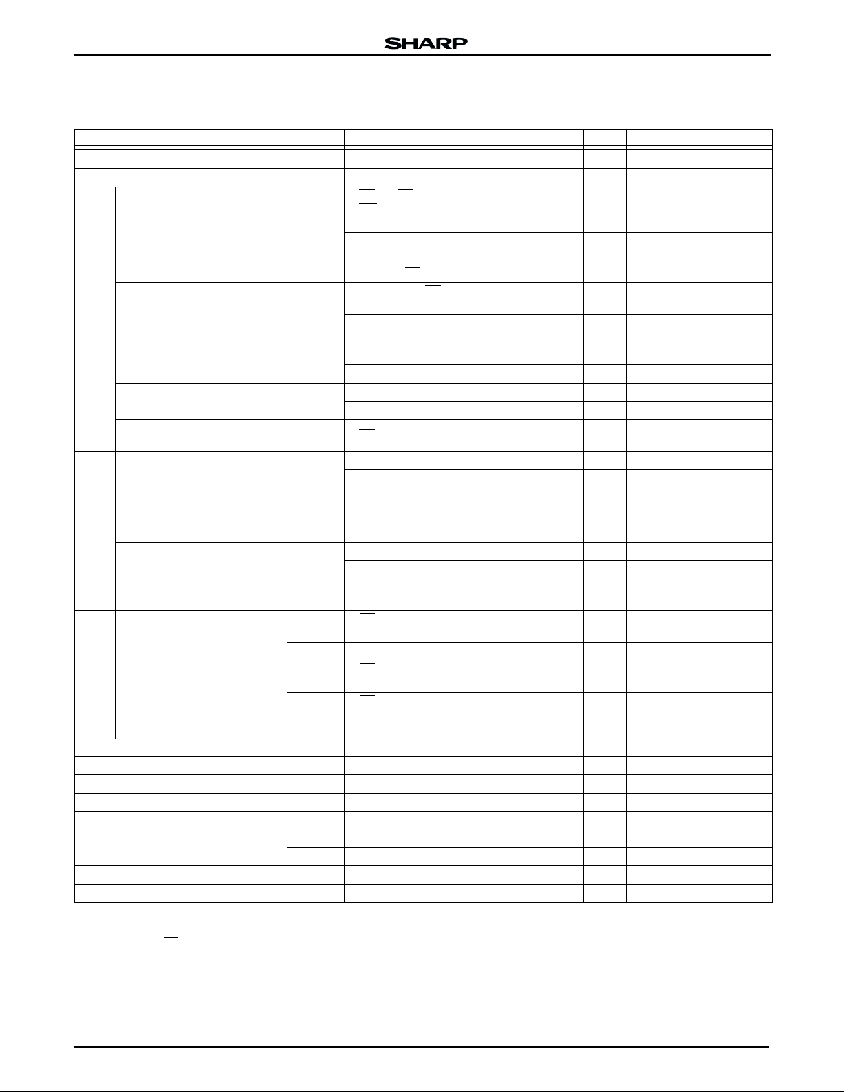
ABSOLUTE MAXIMUM RATINGS
PARAMETER SYMBOL RATINGS UNIT NOTES
Supply voltage V
Input voltage V
Operating temperature T
Storage temperature T
voltage F-V
F-V
PP
voltage F-RP -0.5 to +14.0 V 1, 4, 5
F-RP
NOTES:
1. The maximum applicable voltage on any pins with respect to GND.
2. Except F-V
3. Except F-RP
4. -2.0 V undershoot is allowed when the pulse width is less than 20 ns.
5. +14.0 V overshoot is allowed when the pulse width is less than 20 ns.
PP
.
.
CC
IN
OPR
STG
PP
-0.2 to +3.9 V 1, 2
-0.2 to VCC +0.3 V 1, 3, 4
-25 to +85 °C
-55 to +125 °C
-0.2 to +14.0 V 1, 4, 5
RECOMMENDED DC OPERATING CONDITIONS
TA = -25°C to +85°C
PARAMETER SYMBOL MIN. TYP. MAX. UNIT NOTES
Supply voltage V
Input voltage
CC
V
IH
V
IL
V
HH
2.7 3.0 3.6 V
2.2 VCC + 0.2 V 1
-0.2 0.6 V 2
11.4 12.6 V 3
NOTES:
1. V
is the lower one of S-VCC and F-VCC.
CC
2. -2.0 V undershoot is allowed when the pulse width is less than 20 ns.
3. This voltage is applicable to F-RP
pin only.
PIN CAPACITANCE
TA = 25°C, f = 1 MHz
PARAMETER SYMBOL CONDITION MIN. TYP. MAX. UNIT
Input capacitance* C
I/O capacitance* C
NOTE: *Sampled by not 100% tested.
IN
I/O
VIN = 0 V 20 pF
V
= 0 V 22 pF
I/O
Data Sheet 7
LRS1341/LRS1342 Stacked Chip (16M Flash & 2M SRAM)
DC CHARACTERISTICS
TA = -25°C to + 85°C, VCC = 2.7 V to 3.6 V
1
PARAMETER SYMBOL CONDITION MIN. TYP.
Input leakage current I
Output leakage current I
VIN = VCC or GND -1.5 +1.5 µA
LI
V
LO
= VCC or GND -1.5 +1.5 µA
OUT
F-CE = F-RP = F-VCC ± 0.2 V
F-WP
Standby Current I
Deep Power-Down Current I
CCS
CCD
= F-VCC ± 0.2 V
or F-GND ± 0.2 V
F-CE
= F-RP = V
F-RP = F-GND ± 0.2 V,
(F-RY/BY) = 0 mA
I
OUT
CMOS input, F-CE = F-GND,
Read Current I
F-V
CC
CCR
f = 5 MHz, I
TTL input, F-CE
f = 5 MHz, I
Word Write Current I
Block Erase Current I
Word Write Block Erase
Suspend Current
Standby or Read Current
I
CCWS
I
CCES
I
I
Deep Power-Down Current I
Word Write Current I
F-V
PP
Block Erase Current I
Word Write or Block Erase
Suspend Current
I
PPWS
I
PPES
Standby Current
S-V
CC
I
Operation Current
I
Input LOW Voltage V
Input HIGH Voltage V
Output LOW Voltage V
Output HIGH Voltage (CMOS) V
Lockout during Normal Operations V
F-V
PP
F-V
Word Write or Block Erase
PP
Operations
Lockout Voltage V
F-V
CC
Unlock Voltage V
F-RP
V
V
CCW
PPW
I
F-VPP = 2.7 V to 3.6 V 17 mA
= 11.4 V to 12.6 V 12 mA
F-V
PP
F-VPP = 2.7 V to 3.6 V 17 mA
CCE
= 11.4 V to 12.6 V 12 mA
F-V
PP
F-CE = V
F-VPP = F-V
PPS
PPR
PPD
> F-V
F-V
PP
F-RP = F-GND ± 0.2 V 0.1 5 µA
F-VPP = 2.7 V to 3.6 V 12 40 mA
= 11.4 V to 12.6 V 30 mA
F-V
PP
F-VPP = 2.7 V to 3.6 V 8 25 mA
PPE
= 11.4 V to 12.6 V 20 mA
F-V
PP
F-VPP = V
S-CE1, S-CE2 ≥ S-VCC - 0.2 V
I
SB
or S-CE
S-CE1 = VIH or S-CE2 = V
SB1
S-CE1 = VIL, S-CE2 = VIH, VIN = VIL or
CC1
V
IH
, t
CYCLE
≤ 0.2 V
2
S-CE1 = 0.2 V, S-CE2 = S-VCC - 0.2 V,
V
CC2
IL
IH
OL
OH1IOH
PPLK
PPH1
PPH2
LKO
HH
= S-VCC - 0.2 V, or 0.2 V
IN
= 1 µs, I
t
CYCLE
IOL = 0.5 mA 0.4 V 2
= -0.5 mA 2.2 V 2
Unavailable F-WP 11.4 12.6 V 6
NOTES:
1. Reference values at V
2. Includes F-RY/BY
= 3.0 V and TA = +25°C.
CC
.
3. Automatic Power Savings (APS) for Flash Memory reduces typi to 3 mA at 2.7 VCC in static operation.
cal I
CCR
4. CMOS inputs are either V
are either V
or VIH.
IL
± 0.2 V or GND ± 0.2 V. TTL inputs
CC
OUT
OUT
IH
CC
CC
PPH
= MIN., I
25 50 µA 2
F-WP = VIH or V
IH,
IL
0.2 2 mA
= 0 mA
= F-GND,
= 0 mA
±2 ±15 µA
10 200 µA
10 200 µA
IL
= 0 mA
I/O
= 0 mA
I/O
-0.2 0.6 V
2.2 VCC + 0.2 V
2.7 3.6 V
11.4 12.6 V
1.5 V
5. Block erases and word writes are inhibited when F-V
not guaranteed in the range between V
(MIN.), and above V
6. F-RP
connection to a VHH supply is allowed for a maximum cumu-
PPH
(MAX.).
lative period of 80 hours.
MAX. UNIT NOTES
510µA
25 mA 3, 4
30 mA 3, 4
6mA
45 µA
3mA
45 mA
8mA
1.5 V 5
PP≤VPPLK
(MAX.) and V
PPLK
and
PPH
8 Data Sheet

Stacked Chip (16M Flash & 2M SRAM) LRS1341/LRS1342
FLASH MEMORY AC CHARACTERISTICS
AC Test Conditions
PARAMETER CONDITION
Input pulse level 0 V to 2.7 V
Input rise and fall time 10 ns
Input and Output timing reference level 1.35 V
Output load 1TTL + C
(30 pF)
L
Read Cycle
TA = -25°C to +85°C, VCC = 2.7 V to 3.6 V
PARAMETER SYMBOL MIN. MAX. UNIT
Read Cycle Time t
Address to Output Delay t
F-CE
to Output Delay* t
HIGH to Output Delay t
F-RP
to Output Delay* t
F-OE
F-CE
to Output in LOW-Z t
HIGH to Output in HIGH-Z t
F-CE
to Output in LOW Z t
F-OE
F-OE
HIGH to Output in HIGH-Z t
Output Hold from Address, F-CE
or F-OE change,
whichever occurs first
NOTE: *F-OE may be delayed up to t
ELQV
- t
after the falling edge of F-CE without impact on t
GLQV
AVAV
AVQV
ELQV
PHQV
GLQV
ELQX
EHQZ
GLQX
GHQZ
t
OH
100 ns
100 ns
100 ns
10 µs
45 ns
0ns
45 ns
0ns
20 ns
0ns
.
ELQV
Data Sheet 9

LRS1341/LRS1342 Stacked Chip (16M Flash & 2M SRAM)
Write Cycle (F-WE Controlled)
1
TA = -25°C to +85°C, VCC = 2.7 V to 3.6 V
PARAMETER SYMBOL MIN. MAX. UNIT
Write Cycle Time t
F-RP
HIGH Recovery to F-WE going to LOW t
F-CE Setup to F-WE going LOW t
Pulse Width t
F-WE
F-RP
V
Setup to F-WE going HIGH t
HH
V
F-WP
F-V
Address Setup to F-WE
Data Setup to F-WE
Data Hold from F-WE
Address Hold from F-WE
F-CE
F-WE
F-WE
Setup to F-WE going HIGH t
IH
Setup to F-WE going HIGH t
PP
going HIGH
going HIGH
2
2
HIGH t
HIGH t
Hold from F-WE HIGH t
Pulse Width HIGH t
HIGH to F-RY/BY going LOW t
Write Recovery before Read t
F-V
Hold from Valid SRD, F-RY/BY HIGH-Z t
PP
VHH Hold from Valid SRD, F-RY/BY HIGH-Z t
F-RP
VIH Hold from Valid SRD, F-RY/BY HIGH t
F-WP
AVAV
PHWL
ELWL
WLWH
PHHWH
SHWH
VPWH
t
AVWH
t
DVWH
WHDX
WHAX
WHEH
WHWL
WHRL
WHGL
QVVL
QVPH
QVSL
100 ns
10 µs
0ns
50 ns
100 ns
100 ns
100 ns
50 ns
50 ns
0ns
0ns
0ns
30 ns
100 ns
0ns
0ns
0ns
0ns
NOTES:
1. Read timing characteristics during block erase and word write operations are the same as
during read-only operations. Refer to AC Characteristics for Read Cycle.
2. Refer to the ‘Flash Memory Command Definition’ section for valid A
and DIN for block erase or word write.
IN
10 Data Sheet

Stacked Chip (16M Flash & 2M SRAM) LRS1341/LRS1342
Write Cycle (F-CE Controlled)
1
TA = -25°C to +85°C, VCC = 2.7 V to 3.6 V
PARAMETER SYMBOL MIN. MAX. UNIT
Write Cycle Time t
HIGH Recovery to F-CE going to LOW t
F-RP
Setup to F-CE going LOW t
F-WE
Pulse Width t
F-CE
V
F-RP
F-WP
F-V
Address Setup to F-CE
Data Setup to F-CE
Data Hold from F-CE
Address Hold from F-CE
F-WE
F-CE
F-CE
Write Recovery before Read t
F-V
F-RP
F-WP
Setup to F-CE going HIGH t
HH
V
Setup to F-CE going HIGH t
IH
Setup to F-CE going HIGH t
PP
going HIGH
going HIGH
2
2
HIGH t
HIGH t
Hold from F-CE HIGH t
Pulse Width HIGH t
HIGH to F-RY/BY going LOW t
Hold from Valid SRD, F-RY/BY HIGH-Z t
PP
VHH Hold from Valid SRD, F-RY/BY HIGH-Z t
VIH Hold from Valid SRD, F-RY/BY HIGH t
AVAV
PHEL
WLEL
ELEH
PHEH
SHEH
VPEH
t
AVEH
t
DVEH
EHDX
EHAX
EHWH
EHEL
EHRL
EHGL
QVVL
QVPH
QVSL
100 ns
10 µs
0ns
70 ns
100 ns
100 ns
100 ns
50 ns
50 ns
0ns
0ns
0ns
25 ns
100 ns
0ns
0ns
0ns
0ns
NOTES:
1. Read timing characteristics during block erase and word write operations are the same as
during read-only operations. Refer to AC Characteristics for Read Cycle.
2. Refer to the ‘Flash Memory Command Definition’ section for valid A
and DIN for block erase or word write.
IN
Block Erase and Word Write Performance
TA = -25°C to +85°C, VCC = 2.7 V to 3.6 V
V
= 2.7 V to 3.6 V VPP = 11.4 V to 12.6 V
SYMBOL PARAMETER
t
WHQV1
t
EHQV1
Word Write Time 32K-word Block 55 15 µs 2
Word Write Time 4K-word Block 60 30 µs 2
Block Write Time 32K-word Block 1.8 0.6 s 2
Block Write Time 4K-word Block 0.3 0.2 s 2
t
WHQV2
t
EHQV2
t
WHRZ1
t
EHRZ1
t
WHRZ2
t
EHRZ2
NOTES:
1. Reference values at T
2. Excludes system-level overhead.
Block Erase Time 32K-word Block 1.2 0.7 s 2
Block Erase Time 4K-word Bock 0.5 0.5 s 2
Word Write Suspend Latency Time to Read 7.5 8.6 6.5 7.5 µs
Erase Suspend Latency Time to Read 19.3 23.6 11.8 15 µs
= +25°C and VCC = 3.0 V, VPP = 3.0 V.
A
PP
MIN. TYP.
1
MAX. MIN. TYP.1MAX.
UNIT NOTES
Data Sheet 11

LRS1341/LRS1342 Stacked Chip (16M Flash & 2M SRAM)
FLASH MEMORY AC CHARACTERISTICS TIMING DIAGRAMS
ADDRESS
F-CE
F-OE
F-WE
DQ
Standby
Device
Address Selection
t
GLQV
t
ELQV
t
GLQX
t
ELQX
Address Stable
t
AVAV
Data Valid
Valid Output
t
t
t
OH
EHQZ
GHQZ
HIGH ZHIGH Z
F-V
F-RP
CC
t
AVQV
t
PHQV
Figure 5. Read Cycle Timing Diagram
LRS1342-4
12 Data Sheet

Stacked Chip (16M Flash & 2M SRAM) LRS1341/LRS1342
21 3 4 5 6
ADDRESS
F-WE
F-OE
F-CE
DQ
t
HIGH-Z
t
PHWL
ELWL
A
t
AVAV
t
WLWH
t
DVWH
t
AVWH
A
IN
t
WHAX
t
WHGL
t
WHQV1, 2, 3, 4
D
IN
t
EHRL
Data
Valid
SRD
D
IN
IN
t
WHWL
t
WHEH
t
WHDX
D
IN
F-RY/BY
F-WP
V
HH
V
IH
F-RP
V
IL
V
PPH
F-V
PP
V
PPLK
V
IL
NOTES:
power-up and standby.
1. V
CC
2. Write block erase or word write setup.
3. Write block erase confirm or valid address and data.
4. Automated erase or program delay.
5. Read status register data.
6. Write Read Array command.
Figure 6. Write Cycle Timing Diagram (F-WE Controlled)
t
SHWH
t
PHHWH
t
VPWH
t
t
t
QVVL
QVSL
QVPH
LRS1342-5
Data Sheet 13

LRS1341/LRS1342 Stacked Chip (16M Flash & 2M SRAM)
21 3 4 5 6
ADDRESS
F-WE
F-OE
F-CE
DQ
HIGH-Z
t
PHWL
A
IN
t
AVAV
t
WLELtEHWH
t
ELEH
t
DVEH
D
IN
t
EHEL
t
EHDX
t
AVEH
A
IN
t
EHAX
t
EHGL
t
EHQV1, 2, 3, 4
Data
Valid
SRD
D
IN
t
EHRL
D
IN
F-RY/BY
F-WP
V
HH
V
F-RP
F-V
IH
V
IL
V
PPH
V
PPLK
PP
V
IL
NOTES:
power-up and standby.
1. V
CC
2. Write block erase or word write setup.
3. Write block erase confirm or valid address and data.
4. Automated erase or program delay.
5. Read status register data.
6. Write Read Array command.
Figure 7. Write Cycle Timing Diagram (F-CE Controlled)
t
SHEH
t
PHHEH
t
VPEH
t
QVSL
t
QVPH
t
QVVL
LRS1342-6
14 Data Sheet

Stacked Chip (16M Flash & 2M SRAM) LRS1341/LRS1342
RESET OPERATIONS
TA = -25°C to +85°C, VCC = 2.7 V to 3.6 V
PARAMETER SYMBOL MIN. MAX. UNIT NOTES
F-RP
Pulse LOW Time (if F-RP is tied to VCC, this
specification is not applicable).
F-RP
LOW to Reset during Block Erase or Word Write t
F-V
2.7 V to F-RP HIGH t
CC
NOTES:
1. If F-RP
2. A reset time t
3. When the device power-up, holding F-RP
is asserted while a block erase or word write operation is not executing,
the reset will complete with 100 ns.
is required from the later of F-RY/BY going HIGH-Z, or F-RP going HIGH until outputs are valid.
PHQV
in predefined range and also has been stable there.
HIGH Z
F-RY/BY (R)
V
OL
LOW minimum 100 ns is required after VCC has been
t
PLPH
PLRZ
VPH
100 ns
23.6 µs 1, 2
100 ns 3
F-RP (P)
F-RY/BY (R)
F-RP (P)
F-V
CC
F-RP (P)
V
V
HIGH Z
V
OL
V
V
2.7 V
V
V
V
IH
IL
t
PLPH
A. Reset During Read Array Mode
t
PLRZ
IH
IL
t
PLPH
B. Reset During Block Erase or Word Write
IL
IH
IL
t
VPH
C. F-RP Rising Timing
LRS1342-7
Figure 8. AC Waveform for Reset Operation
Data Sheet 15

LRS1341/LRS1342 Stacked Chip (16M Flash & 2M SRAM)
SRAM AC ELECTRICAL CHARACTERISTICS
AC Test Conditions
PARAMETER CONDITION
Input Pulse Level 0.4 V to 2.7 V
Input Rise and Fall Time 5 ns
Input and Output Timing Reference Level 1.5 V
Output Load* 1TTL + C
NOTE: *Including scope and jig capacitance.
(30 pF)
L
Read Cycle
TA = -25°C to +85°C, VCC = 2.7 V to 3.6 V
PARAMETER SYMBOL MIN. MAX. UNIT
Read Cycle Time t
Address Access Time t
Chip Enable Access Time
S-CE
S-CE
1
2
t
ACE1
t
ACE2
Byte Enable Access Time t
Output Enable to Output Valid t
Output hold from address change t
S-CE
S-CE
, S-CE2 LOW to Output Active*
1
LOW to Output Active* t
S-OE
or S-LB LOW to Output in HIGH Impedance* t
S-UB
, S-CE2 HIGH to Output in HIGH Impedance*
S-CE
1
HIGH to Output in HIGH Impedance* t
S-OE
or S-LB HIGH to Output in HIGH Impedance* t
S-UB
NOTE: *Active output to HIGH impedance and HIGH impedance to output active
tests specified for a ±200 mV transition from steady state levels into the test load.
S-CE
S-CE
S-CE
1
2
1
2
t
t
t
t
OHZ
RC
AA
BE
OE
OH
LZ1
LZ2
OLZ
BLZ
HZ1
HZ2
BHZ
85 ns
85 ns
85 ns
85 ns
85 ns
45 ns
10 ns
10 ns
10 ns
10 ns
10 ns
025ns
025ns
025ns
025ns
Write Cycle
TA = -25°C to +85°C, VCC = 2.7 V to 3.6 V
PARAMETER SYMBOL MIN. MAX. UNIT
Write Cycle Time t
Chip Enable to End of Write t
Address Valid to End of Write t
Byte Enable to End of Write t
Address Setup Time t
Write Pulse Width t
Write Recovery Time t
Input Data Setup Time t
Input Data Hold Time t
HIGH to Output Active* t
S-WE
LOW to Output in HIGH Impedance* t
S-WE
NOTE: *Active output to HIGH impedance and HIGH impedance to output active
tests specified for a ±200 mV transition from steady state levels into the test load.
WC
CW
AW
BW
AS
WP
WR
DW
DH
OW
WZ
16 Data Sheet
85 ns
75 ns
75 ns
75 ns
0ns
65 ns
0ns
35 ns
0ns
5ns
025ns

Stacked Chip (16M Flash & 2M SRAM) LRS1341/LRS1342
SRAM AC CHARACTERISTICS TIMING DIAGRAMS
t
RC
ADDRESS
t
AA
t
ACE1, 2
S-CE
1
S-CE
2
S-UB, S-LB
S-OE
D
OUT
NOTE: S-WE is HIGH for Read Cycle.
t
LZ
t
BE
t
BLZ
t
OE
t
OLZ
Data Valid
Figure 9. Read Cycle Timing Diagram
t
HZ
t
HZ
t
BHZ
t
OHZ
t
OH
LRS1342-8
Data Sheet 17

LRS1341/LRS1342 Stacked Chip (16M Flash & 2M SRAM)
t
WC
ADDRESS
t
AW
t
CW
(NOTE 2)
S-CE
1
t
WR
S-CE
2
t
BW
(NOTE 3)
S-UB, S-LB
t
AS
(NOTE 4)
(NOTE 7)
S-WE
t
WZ
D
OUT
(NOTE 6)
D
IN
NOTES:
1. A write occurs during the overlap of a LOW S-CE
A write begins at the latest transition among S-CE
and
S-WE going LOW. A write ends at the earliest transition among S-CE1 going HIGH,
S-CE2 going LOW and S-WE going HIGH. tWP is measured from the beginning of
write to the end of write.
2. t
is measured from the later of S-CE1 going LOW or S-CE2 going HIGH to the end
CW
of write.
3. t
is measured from the time of going LOW S-UB or LOW S-LB to the end of write.
BW
4. t
is measured from the address valid to the beginning of write.
AS
5. t
is measured from the end of write to the address change.
WR
6. During this period, DQ pins are in the output state, therefore the input signals of
opposite phase to the outputs must not be applied.
7. If S-CE
after S-WE going LOW, the outputs remain in HIGH impedance state.
8. If S-CE
S-WE going HIGH, the outputs remain in HIGH impedance state.
goes LOW or S-CE2 goes HIGH simultaneously with S-WE going LOW or
1
goes HIGH or S-CE2 goes LOW simultaneously with S-WE going HIGH or
1
, a HIGH S-CE2 and a LOW S-WE.
1
going LOW, S-CE2 going HIGH
1
Figure 10. Write Cycle Timing Diagram (S-WE Controlled)
t
WP
t
DW
t
WR
(NOTE 5)
t
OW
(NOTE 8)
t
DH
Data Valid
LRS1342-9
18 Data Sheet

Stacked Chip (16M Flash & 2M SRAM) LRS1341/LRS1342
t
WC
ADDRESS
t
AW
t
WP
t
CW
(NOTE 2)
t
BW
(NOTE 3)
t
WR
t
WR
(NOTE 5)
S-CE
S-CE
S-UB, S-LB
t
AS
(NOTE 4)
1
2
(NOTE 7)
S-WE
D
OUT
D
IN
HIGH IMPEDANCE
(NOTE 6)
NOTES:
1. A write occurs during the overlap of a LOW S-CE
A write begins at the latest transition among S-CE
and
S-WE going LOW. A write ends at the earliest transition among S-CE1 going HIGH,
S-CE2 going LOW and S-WE going HIGH. tWP is measured from the beginning of
write to the end of write.
2. t
is measured from the later of S-CE1 going LOW or S-CE2 going HIGH to the end
CW
, a HIGH S-CE2 and a LOW S-WE.
1
going LOW, S-CE2 going HIGH
1
of write.
3. t
is measured from the time of going LOW S-UB or LOW S-LB to the end of write.
BW
4. t
is measured from the address valid to the beginning of write.
AS
5. t
is measured from the end of write to the address change.
WR
6. During this period, DQ pins are in the output state, therefore the input signals of
opposite phase to the outputs must not be applied.
7. If S-CE
goes LOW or S-CE2 goes HIGH simultaneously with S-WE going LOW or
1
after S-WE going LOW, the outputs remain in HIGH impedance state.
Figure 11. Write Cycle Timing Diagram (S-CE Controlled)
t
DW
Data Valid
t
DH
LRS1342-10
Data Sheet 19

LRS1341/LRS1342 Stacked Chip (16M Flash & 2M SRAM)
t
WC
ADDRESS
t
AW
t
CW
(NOTE 2)
S-CE
1
t
WR
S-CE
2
t
BW
(NOTE 3)
S-UB, S-LB
t
AS
(NOTE 4)
(NOTE 7)
S-WE
t
WZ
D
OUT
(NOTE 6)
D
IN
NOTES:
1. A write occurs during the overlap of a LOW S-CE
A write begins at the latest transition among S-CE
and
S-WE going LOW. A write ends at the earliest transition among S-CE1 going HIGH,
S-CE2 going LOW and S-WE going HIGH. tWP is measured from the beginning of
write to the end of write.
2. t
is measured from the later of S-CE1 going LOW or S-CE2 going HIGH to the end
CW
, a HIGH S-CE2 and a LOW S-WE.
1
going LOW, S-CE2 going HIGH
1
of write.
3. t
is measured from the time of going LOW S-UB or LOW S-LB to the end of write.
BW
4. t
is measured from the address valid to the beginning of write.
AS
5. t
is measured from the end of write to the address change.
WR
6. During this period, DQ pins are in the output state, therefore the input signals of
opposite phase to the outputs must not be applied.
7. If S-CE
goes LOW or S-CE2 goes HIGH simultaneously with S-WE going LOW or
1
after S-WE going LOW, the outputs remain in HIGH impedance state.
8. If S-CE
goes HIGH or S-CE2 goes LOW simultaneously with S-WE going HIGH or
1
S-WE going HIGH, the outputs remain in HIGH impedance state.
Figure 12. Write Cycle Timing (S-UB, S-LB Controlled)
t
WP
t
DW
t
WR
(NOTE 5)
t
OW
(NOTE 8)
t
DH
Data Valid
LRS1342-11
20 Data Sheet

Stacked Chip (16M Flash & 2M SRAM) LRS1341/LRS1342
SRAM DATA RETENTION CHARACTERISTICS
TA = -25°C to +85°C
PARAMETER SYMBOL CONDITIONS MIN. TYP.1MAX. UNIT NOTES
Data Retention Supply Voltage V
Data Retention Supply Current I
Chip Enable Setup Time t
Chip Enable Hold Time t
NOTES:
1. Reference value at T
2. S-CE
≥ VCC - 0.2 V, S-CE2 ≥ VCC - 0.2 V (S-CE1 controlled) or S-CE2 ≤ 0.2 V (S-CE2 controlled).
1
S-V
CC
S-CE
1
= 25°C, S-VCC = 3.0 V.
A
2.7 V
2.2 V
V
CCDR
CCDR
CCDR
CDR
R
t
CDR
S-CE2 ≤ 0.2 V or
S-CE
≥ V
1
CCDR
V
= 3V, S-CE2 ≤ 0.2 V or
CCDR
S-CE
≥ V
1
CCDR
Data Retention Mode
S-CE1 ≥ V
- 0.2 V
- 0.2 V
CCDR
- 0.2 V
2.0 3.6 V 2
35 µA 2
0ns
5ms
t
R
0 V
NOTE: To control the data retention mode at S-CE
V
CCDR
and V
- 0.2 V, or 0 V and 0.2 V, and during the data retention mode.
CCDR
Figure 13. Data Retention Timing Diagram (S-CE1 Controlled)
S-V
CC
2.7 V
S-CE
2
V
CCDR
t
CDR
0.6 V
0 V
Figure 14. Data Retention Timing Diagram (S-CE
, fix the input level of S-CE2 between
1
Data Retention Mode
S-CE2 ≤ 0.2 V
t
R
Controlled)
2
LRS1342-12
LRS1342-13
Data Sheet 21

LRS1341/LRS1342 Stacked Chip (16M Flash & 2M SRAM)
GENERAL DESIGN GUIDELINES
Supply Power
Maximum difference (between F-VCC and S-VCC) of
the voltage is less than 0.3 V.
Power Supply and Chip Enable of Flash
Memory and SRAM
S-CE1 should not be LOW and S-CE2 should not be
HIGH when F-CE
If the two memories are active together, they may
not operate normally because of interference noises or
data collision on DQ bus.
Both F-V
recommended supply voltage at the same time except
SRAM data retention mode.
is LOW simultaneously.
and S-VCC need to be applied by the
CC
Power Up Sequence
When turning on Flash memory power supply, keep
LOW. After F-VCC reaches over 2.7 V, keep F-RP
F-RP
LOW for more than 100 ns.
Device Decoupling
The power supply needs to be designed carefully
because one of the SRAM and the Flash Memory is in
standby mode when the other is active. A careful
decoupling of power supplies is necessary between
SRAM and Flash Memory. Note peak current caused
by transition of control signals (F-CE
, S-CE1, S-CE2).
FLASH MEMORY DATA PROTECTION
Noises having a level exceeding the limit specified in
the specification may be generated under specific
operating conditions on some systems.
Such noises, when induced onto F-WE
power supply may be interpreted as false commands,
causing undesired memory updating.
To protect the data stored in the flash memory
against unwanted overwriting, systems operating with
the flash memory should have the following write protect designs, as appropriate:
signal or
Protecting Data in Specific Block
By setting a F-WP to LOW, only the boot block can
be protected against overwriting. Parameter and main
blocks cannot be locked. System program, etc., can be
locked by storing them in the boot block. When a high
voltage is applied to F-RP
enabled for all blocks.
For further information on setting/resetting of block
bit, and controlling of F-WP
‘Command Definitions’ section.
, overwrite operation is
and F-RP, refer to the
Data Protection Through F-V
When the level of F-VPP is lower than F-V
out voltage), write operation on the flash memory is disabled. All blocks are locked and the data in the blocks
are completely write protected.
For the lockout voltage refer to the ‘DC Characteristics’ section.
PP
PPLK
(lock-
Data Protection During Voltage Transition
DATA PROTECTION THROUGH F-RP
When the F-RP is kept LOW during power up and
power down sequence, write operation on the flash
memory is disabled, write protecting all blocks.
For details of F-RP
Memory AC Electrical Characteristics’ section.
control refer to the ‘Flash
DESIGN CONSIDERATIONS
Power Supply Decoupling
To avoid a bad effect on the system by flash memory
power switching characteristics, each device should
have a 0.1 µF ceramic capacitor connected between its
and GND and between its VPP and GND. LOW
V
CC
inductance capacitors should be placed as close as
possible to package leads.
VPP Trace on Printed Circuit Boards
Updating the memory contents of flash memories
that reside in the target system requires that the printed
circuit board designer pay attention to the V
Supply trace. Use similar trace widths and layout considerations given to the V
power bus.
CC
Power
PP
The Inhibition of Overwrite Operation
Please do not execute reprogramming ‘0’ for the bit
which has already been programmed ‘0’. Overwrite
operation may generate unerasable bit. In case of
reprogramming ‘0’ to the data which has been programmed ‘1’.
• Program ‘0’ for the bit in which you want to change
data from ‘1’ to ‘0’.
• Program ‘1’ for the bit which has already been pro-
grammed ‘0’.
For example, changing data from
‘1011110110111101’ to ‘1010110110111100’ requires
‘1110111111111110’ programming.
Power Supply
Block erase, full chip erase, word write and lock-bit
configuration with an invalid V
tics’) produce spurious results and should not be
attempted. Device operations at invalid V
product spurious results and should be attempted.
(see ‘DC Characteris-
PP
voltage
CC
22 Data Sheet

Stacked Chip (16M Flash & 2M SRAM) LRS1341/LRS1342
OUTLINE DIMENSIONS
FBGA072-P-0811
B
TOP VIEW
SIDE VIEW
S
A
0.10 S
INDEX
0.10 S
11.0
+0.2
-0
+0.2
-0
8.0
(See Detail)
0.40 TYP.
DETAIL
1.1 TYP.
0.8 TYP.
H
BOTTOM VIEW
D
NOTE: Dimensions are in mm.
G
F
E
D
C
B
A
12345678
0.4 TYP.
C
9101112
φ 0.45 ±0.05
φ 0.30
φ 0.15
1.2 TYP.
0.8 TYP.
M
SSAB
M
1.4 MAX.
0.35 ±0.05
0.4 TYP.
CD
72FBGA
Data Sheet 23

LRS1341/LRS1342 Stacked Chip (16M Flash & 2M SRAM)
LIFE SUPPORT POLICY
SHARP components should not be used in medical devices with life support functions or in safety equipment (or similiar applications where
component failure would result in loss of life or physical harm) without the written approval of an officer of the SHARP Corporation.
LIMITED WARRANTY
SHARP warrants to its Customer that the Products will be free from defects in material and workmanship under normal use and service for a
period of one year from the date of invoice. Customer's exclusive remedy for breach of this warranty is that SHARP will either (i) repair or
replace, at its option, any Product which fails during the warranty period because of such defect (if Customer promptly reported the failure to
SHARP in writing) or, (ii) if SHARP is unable to repair or replace, refund the purchase price of the Product upon its return to SHARP. This
warranty does not apply to any Product which has been subjected to misuse, abnormal service or handling, or which has been altered or
modified in design or construction, or which has been serviced or repaired by anyone other than Sharp. The warranties set forth herein are in
lieu of, and exclusive of, all other warranties, express or implied. ALL EXPRESS AND IMPLIED WARRANTIES, INCLUDING THE
WARRANTIES OF MERCHANTABILITY, FITNESS FOR USE AND FITNESS FOR A PARTICULAR PURPOSE, ARE SPECIFICALLY
EXCLUDED. In no event will Sharp be liable, or in any way responsible, for any incidental or consequential economic or property damage.
The above warranty is also extended to Customers of Sharp authorized distributors with the following exception: reports of failures of Products
during the warranty period and return of Products that were purchased from an authorized distributor must be made through the distributor.
In case Sharp is unable to repair or replace such Products, refunds will be issued to the distributor in the amount of distributor cost.
SHARP reserves the right to make changes in specifications at any time and without notice. SHARP does not assume any responsibility
for the use of any circuitry described; no circuit patent licenses are implied.
NORTH AMERICA
SHARP Microelectronics
of the Americas
5700 NW Pacific Rim Blvd.
Camas, WA 98607, U.S.A.
Phone: (360) 834-2500
Telex: 49608472 (SHARPCAM)
Facsimile: (360) 834-8903
EUROPE
SHARP Electronics (Europe) GmbH
Microelectronics Division
Sonninstraße 3
20097 Hamburg, Germany
Phone: (49) 40 2376-2286
Facsimile: (49) 40 2376-2232
http://www.sharpmed.com
ASIA
SHARP Corporation
Integrated Circuits Group
2613-1 Ichinomoto-Cho
Tenri-City, Nara, 632, Japan
Phone: +81-743-65-1321
Facsimile: +81-743-65-1532
http://www.sharp.co.jp
http://www.sharpsma.com
©1999 by SHARP Corporation Reference Code SMA99092
 Loading...