Data Sheet
LRS1338A-1
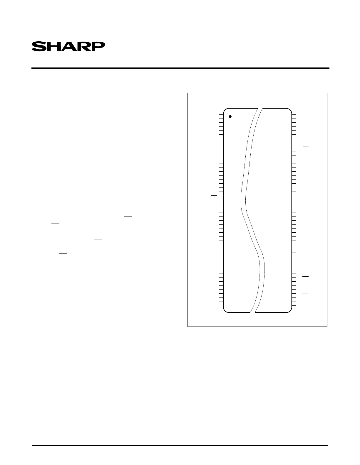
TOP VIEW48-PIN TSOP
2
3
4
5
8
9
S-A
9
/F-A
8
S-A12/F-A
11
S-A13/F-A
12
S-A14/F-A
13
48
45
42
6
7S-A
10
/F-A
9
S-A11/F-A
10
47
46
I/O
14
S-CE
I/O
15
I/O
13
10
11
12
I/O
7
13
44
I/O
3
43
I/O
10
I/O
6
14
15
16
17
18
19
20
39
36
41
40
38
37
I/O
1
S-WE
I/O
8
S-A7/F-A
6
S-A6/F-A
5
S-A8/F-A
7
F-A18
F-A17
F-WP
S-A
5
/F-A
4
I/O
0
F-OE
I/O
5
I/O
4
I/O
12
I/O
9
1
S-A
15
/F-A
14
S-A16/F-A
15
S-A17/F-A
16
21
22
23
24S-A
0
S-A2/F-A
1
S-A4/F-A
3
S-A3/F-A
2
34
F-CE
35
GND
31
33
32
30
29
S-A
1
/F-A
0
F-RP
F-WE
S-OE
F-V
PP
S-V
CC
F-V
CC
I/O
11
I/O
2
27
28
26
25
LRS1338A
Stacked Chip
8M Flash Memory and 2M SRAM
FEATURES
PIN CONFIGURATION
• Flash memory and SRAM
• Stacked die chip scale package
• 48-pin TSOP (TSOP48-P-1014) plastic package
• Power supply: 2.7 V to 3.6 V
• Operating temperature: -40°C to +85°C
• Access time (MAX.):
– Flash memory: 120 ns
– SRAM: 85 ns
• Operating current (MAX.):
–Flash memory
– Read: 25 mA (t
– Word write: 57 mA (F -V
– Block erase: 42 mA (F-V
– SRAM: 25 mA (t
• Standby current
2
CYCLE
CYCLE
= 200 ns)
≥ 3.0 V)
CC
≥ 3.0 V)
CC
= 200 ns)
– Flash memory: 20 µA MAX. (F-CE ≥ F-VCC - 0.2 V,
F-RP
≤ 0.2 V, F-VPP ≤ 0.2 V)
–SRAM:
– 40 µA MAX. (S-CE
• Fully static operation
• Three-state output
NOTES:
1. Block erase and word write operations of flash memory with
2. Total standby current is the summation of flash’s memory standby
DESCRIPTION
as 524,288 × 16-bit flash memory and 262,144 × 8-bit
static RAM in one package. It is fabricated using silicongate CMOS process technology.
S-CE
< -30°C are not supported.
T
A
current and SRAM’s one.
The LRS1338A is a combination memory organized
≥ S-VCC - 0.2 V)
– 0.6 µA TYP. (T
A
≥ S-VCC - 0.2 V)
= 25°C, S-VCC = 3 V,
Figure 1. LRS1338A Pin Configuration
Data Sheet 1
LRS1338A Stacked Chip (8M Flash & 2M SRAM)
CC
SRAM
S-V
F-V
CC
F-CE
F-OE
F-WE
F-RP
F-WP
, F-A
F-A
17
S-A1 to S-A
F-A
to F-A
0
S-A
S-CE
S-OE
S-WE
F-V
524,288 x 16 BIT
FLASH MEMORY
18
17
,
16
0
262,144 x 8 BIT
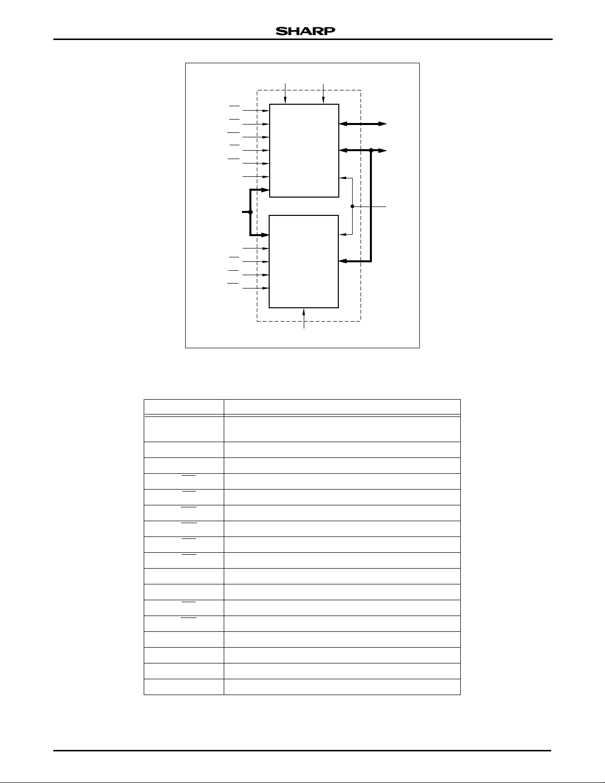
Figure 2. LRS1338A Block Diagram
PP
I/O8 to
I/O
15
I/O0 to
I/O
7
GND
LRS1338A-2
Table 1. Pin Descriptions
PIN DESCRIPTION
S-A
to S-A
1
F-A0 to F-A
S-A
F-A
17
F-CE
S-CE
F-WE
S-WE
F-OE
S-OE
I/O
0
I/O
to I/O
8
F-RP
F-WP
F-V
F-V
S-V
0
to F-A
to I/0
CC
PP
CC
17
Common Address Input Pins
16
Address Input Pin for SRAM
Address Input Pin for Flash Memory
18
Chip Enable Input Pin for Flash Memory
Chip Enable Input Pin for SRAM
Write Enable Input Pin for Flash Memory
Write Enable Input Pin for SRAM
Output Enable Input Pin for Flash Memory
Output Enable Input Pin for SRAM
Common Data Input/Output Pins
7
Data Input/Output Pins for Flash Memory
15
Reset/Deep Power Down Input Pin for Flash Memory
Write Protect Pin for Flash Memory’s Boot Block
Power Supply Pin for Flash Memory
Power Supply Pin for Flash Memory Write/Erase
Power Supply Pin for SRAM
GND Common Ground
2 Data Sheet
Stacked Chip (8M Flash & 2M SRAM) LRS1338A
GENERAL DESIGN GUIDELINES
Supply Po wer
Maximum difference (between F-VCC and S-VCC) of
the voltage is less than 0.3 V.
Power Supply and Chip Enable of Flash
Memory and SRAM
It is forbidden that both F-CE and S-CE should be
LOW simultaneously. If the two memories are active
together, they many not op erate nor mally du e to inter ference noi ses or dat a collis ion on I/O bus. Bot h F-V
CC
and S-VCC need to be applied by the recommende d
supply voltage at the same time except SRAM data
retention mode.
SRAM Data Retention
SRAM data retention is capable in three ways.
SRAM power switching betwee n a system bat tery an d
a backup battery needs careful device decoupling from
Flash Memory to prevent SRAM supply voltage from
falling lower than 2.0 V by a Flash Mem ory peak current caused by transitio n of F la sh Mem or y supp ly vol tage or of control signals (F-CE
CASE 1: FLASH MEMORY IS IN STANDBY MODE
(F-V
= 2.7 V TO 3.6 V)
CC
• SRAM inputs and input/outputs except S-CE
be applied with voltages in the range of -0.3 V to
S-V
+ 0.3 V or to be open (HIGH-Z).
CC
• Flash Memory inputs and input/outputs except F-CE
and RP need to be applied with voltages in the range
of -0.3 V to S-V
+ 0.3 V or to be open (HIGH-Z).
CC
, F-OE, and RP).
need to
CASE 2: FLASH MEMORY IS IN DEEP POWER
DOWN MODE (F-V
• SRAM inputs and input/outputs except S-CE
= 2.7 V TO 3.6 V)
CC
need to
be applied with voltages in the range of -0.3 V to
S-V
+ 0.3 V or to be open.
CC
• Flash Memory inputs and input/outputs except RP
need to be applied with voltages in the range of -0.3 V
to S-V
be at the same level as F-V
+ 0.3 V or to be open (HIGH-Z). RP needs to
CC
or to be open.
CC
CASE 3: FLASH MEMORY POWER SUPPLY IS
TURNED OFF (F-V
• Fix RP
LOW level before tu rning off Flash memo ry
CC
= 0 V)
power supply.
• SRAM inputs and input/outputs except S-CE
need to
be applied with voltages in the range of -0.3 V to
S-V
+ 0.3 V or to be open (HIGH-Z).
CC
• Flash Memory inputs and input/outputs except RP
need to be applied with voltages in the range of
-0.3 V to S-V
+ 0.3 V or to be open (HIGH-Z).
CC
Power Up Sequence
When turning on Flash memory power supply, keep
RP
LOW. After F-VCC reaches ove r 2.7 V, keep RP
LOW for more than 100 ns.
Device Decoupling
The power supply needs to be designed c arefully
because one of the SRAM and the F lash Me mor y is in
standby mode when the other is active. A careful
decoupling of power supplies is necessary between
SRAM and Flash Memory. Note peak current caused
by transition of control signals (F-CE
, S-CE).
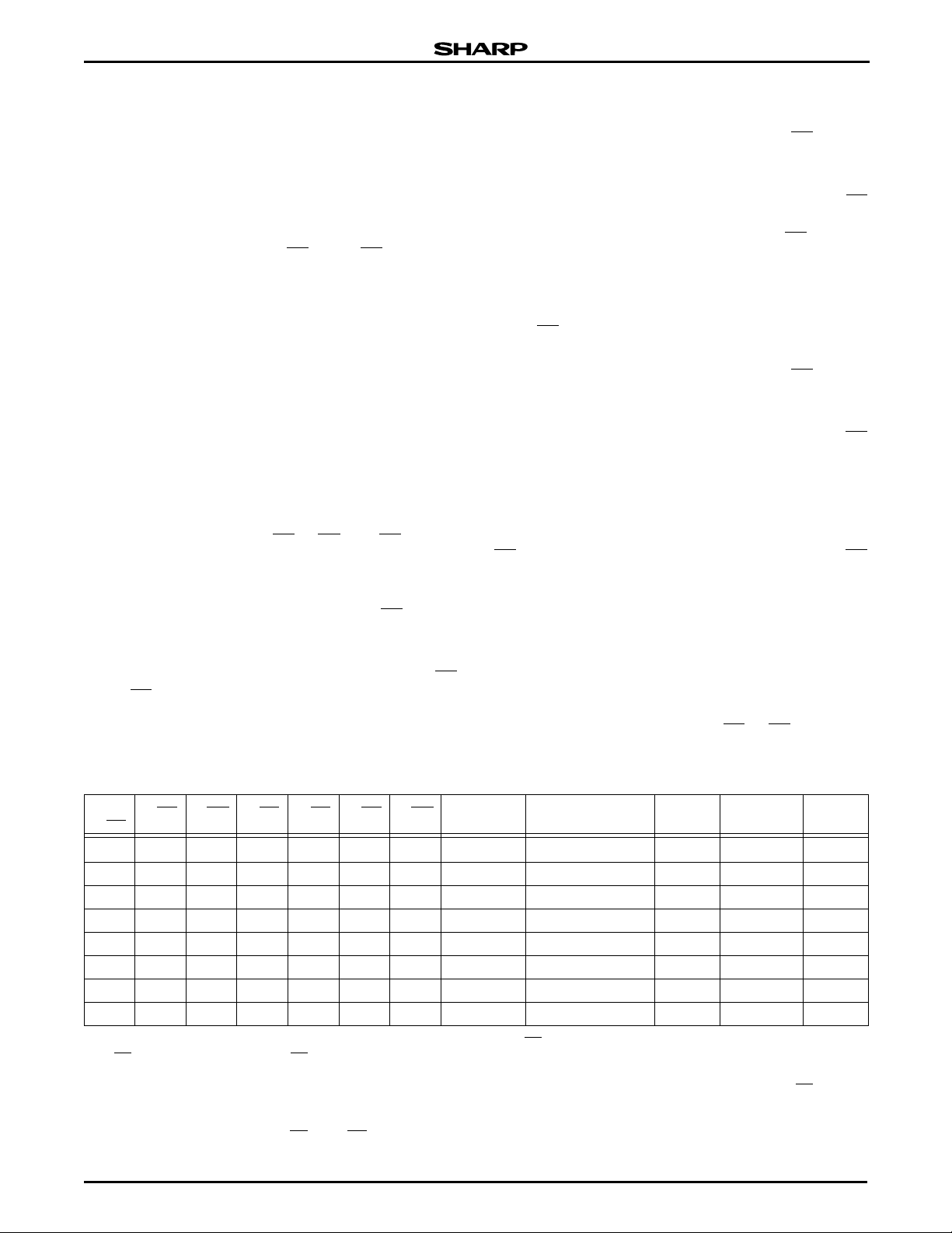
Table 2. Truth Table
F-CE F-OE F-WE F-RP S-CE S-OE S-WE ADDRESS MODE
L L H H H X X X Flas h read Output I
L H H H H X X X Flash read HIGH-Z I
LHLHHXX XFlash write Input I
H X X X L L H X SRAM read Output I
H X X X L H H X SRAM read HIGH-Z I
H X X X L X L X SRAM write Input I
H X X H H X X X Standby HIGH-Z I
X X X L H X X X Deep power down HIGH-Z I
NOTES:
1. F-CE
2. X can be V
3. Refer to DC Characteristics. When F-V
4. Do not use in a timing that both F-OE
should not be LOW when S-CE is LOW simultaneously.
or VIH for control pins and addresses, and V
for F-VPP. See DC Characteristics for V
tents can be read, but not altered.
IL
or V
and V
PPLK
≤ V
PP
and F-WE is LOW level.
PPLK
voltages.
PPH
, memory con-
PPLK
PPH
5. F-RP
6. Command writes involving block erase, write, or lock-bit configura-
7. Refer to Table 6 for valid D
1,2
to
I/O
0
I/O
at GND ± 0.2 V ensures the lowest deep power down current.
tion are reliably executed whe n F-V
block erase or word w rite operations wit h VIH < F-RP < VHH or
T
<-30°C produce spurious results and should not be attempted.
A
during a write operation.
IN
CURRENT NOTE
15
CC
CC
CC
CC
CC
CC
SB
SB
= V
PP
and F-VCC=V
PPH
3, 4
5
4, 6, 7
5
CC1
Data Sheet 3
LRS1338A Stacked Chip (8M Flash & 2M SRAM)
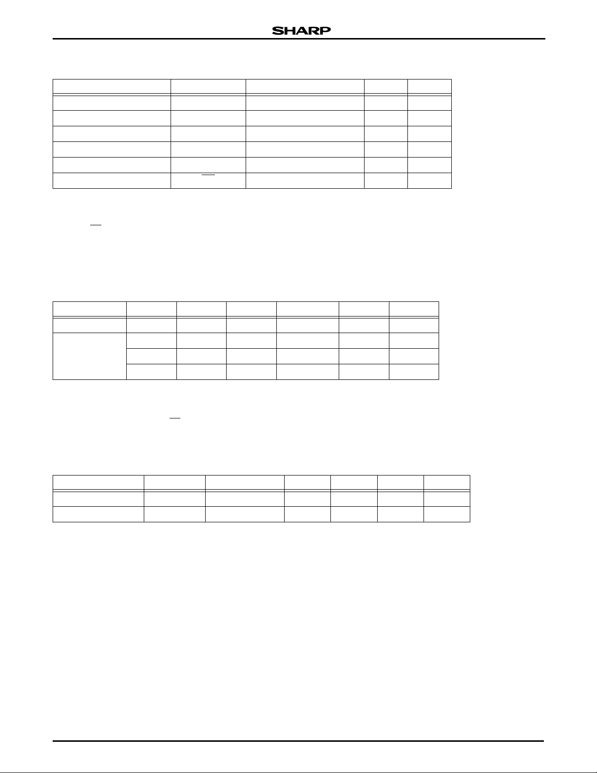
ABSOLUTE MAXIMUM RATINGS
PARAMETER SYMBOL RATINGS UNIT NOTES
Supply voltage V
Input voltage V
Operating temperature T
Storage temperature T
voltage V
V
PP
CC
IN
OPR
STG
PP
Input voltage RP
NOTES:
1. The maximum applicable voltage on any pins with respect to GND.
2. Except V
3. Except RP
4. -2.0 V undershoot is allowed when the pulse width is less than 20 ns.
5. +14.0 V overshoot is allowed when the pulse width is less than 20 ns.
PP
.
.
-0.2 to +4.6 V 1, 2
-0.3 to VCC +0.3 V 1, 3, 4
-40 to +85 °C
-65 to +125 °C
-0.2 to +12.6 V 1, 5
-0.5 to +12.6 V 1, 4, 5
RECOMMENDED DC OPERATING CONDITIONS
TA = -40°C to +85°C
PARAMETER SYMBOL MIN. TYP. MAX. UNIT NOTES
Supply voltage V
Input voltage
CC
V
IH
V
IL
V
HH
2.7 3.0 3.6 V
2.0 VCC + 0.3 V 1
-0.3 0.8 V 2
11.4 12.6 3
NOTES:
1. V
is the lower one of S-VCC and F-VCC.
CC
2. -2.0 V undershoot is allowed when the pulse width is less than 20 ns.
3. This voltage is applicable to F-RP
pin only.
PIN CAPACITANCE
TA = 25°C, f = 1 MHz
PARAMETER SYMBOL CONDITION MIN. TYP. MAX. UNIT
Input capacitance* C
I/O capacitance* C
NOTE: *
Sampled by not 100% tested.
IN
I/O
VIN = 0 V 20 pF
V
= 0 V 22 pF
I/O
4 Data Sheet
Stacked Chip (8M Flash & 2M SRAM) LRS1338A
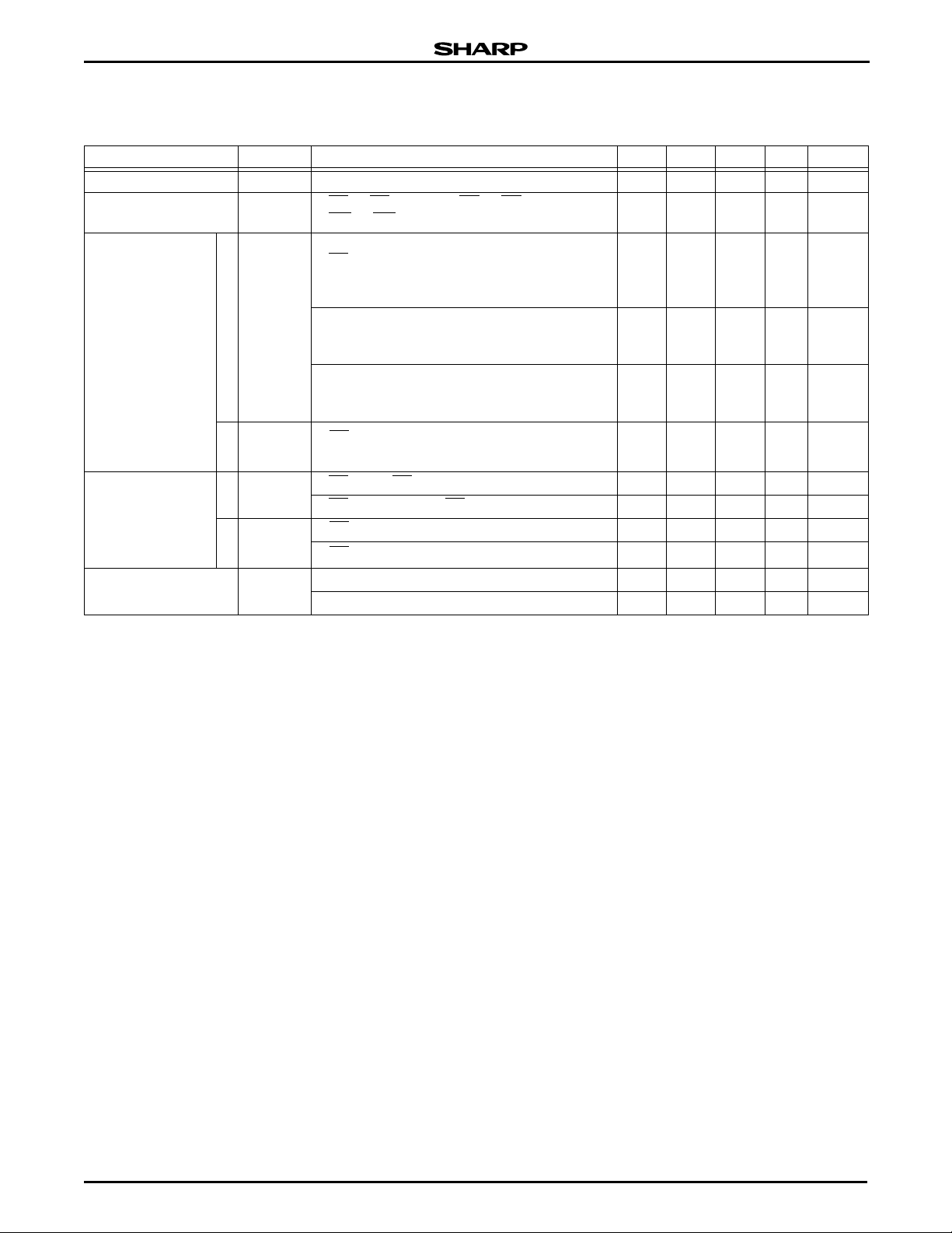
DC ELECTRICAL CHARACTERISTICS
TA = -40°C to + 85°C, VCC = 2.7 V to 3.6 V
PARAMETER SYMBOL CONDITION MIN. TYP. MAX. UNIT NOTES
Input leakage current I
Output leakage current I
Operating supply
current
I
Flash
I
SRAM
I
Standby current
Flash
I
SRAM
Output voltage
NOTES:
1. This value is read current (I
2. Sampled but not 100% tested.
3. This value is operation current (I
4. This value is operation current (I
5. This value is operation current (I
VOL,
V
CCR
CC
CC
VIN = 0V to V
LI
F-CE, S-CE = VIH or F-OE, S-OE = VIH or
LO
, S-WE = VIH, V
F-WE
CC
= 0 V to V
I/O
CC
-1.5 1.5 µA
-1.5 1.5 µA
Read current, F-VPP ≤ F-VCC,
≤ 0.2 V, VIN ≥ VCC – 0.2 V or
F-CE
V
≤ 0.2 V
IN
= 200 ns, I
t
CYCLE
Summation of V
rent, and V
F-V
≥ 3.0 V
CC
PP
Summation of V
lock-bits current, and V
Block lock-bits current. F-V
= 0 mA
I/O
Byte Write or set l ock-bi t c ur-
CC
Byte Write or set lock-bit current.
Block Erase or Clear Block
CC
Block Erase or Clear
PP
≥ 3.0 V
CC
S-CE = 0.2 V, VIN ≥ VCC – 0.2 V or VIN ≥ 0.2 V
t
CYCLE
F-CE = VIH, RP = V
SB
F-CE
S-CE = V
SB
S-CE
= 200 ns, I
≥ VCC – 0.2 V, RP ≤ 0.2 V 20 µA 7
IH
≥ VCC – 0.2 V 0.6 40 µA 9, 10
= 0 mA
I/O
IH
IOL = 2.0 mA 0.4 V
I
OH
+ I
CCW
CCE
CC1
= 1.0 mA 2.4 V
OH
) of flash memory.
PPR
+ I
) of flash memory.
PPW
+ I
) of flash memory.
PPE
) of SRAM.
6. This value is standby current (I
7. This value is deep power down current (I
flash memory.
8. This value is standby current (I
9. This value is standby current (I
10.Reference values at V
CCS
SB1
SB
= 3.0 V and TA = +25°C
CC
25 mA 1
57 mA 2, 3
42 mA 2, 4
25 mA 5
2.0 mA 6
3.0 mA 8
+ I
) of flash memory.
PPS
CCD
) of SRAM
) of SRAM.
+ I
PPD
) of
Data Sheet 5

LRS1338A Stacked Chip (8M Flash & 2M SRAM)
FLASH MEMORY*
New Features
The LRS1388A flash memory ma intain s backw ards
compatibility with SHARP’s LH28F 800B G- L.
• SmartVoltage technolog y
• Enhanced suspend capabilities
• Boot block architecture
Please note the following important differences:
• V
has been lowered to 1.5 V to support 3.0 V
PPLK
block erase and word write operations. Designs that
switch V
sure that the V
• Allow V
off during read ope rations should ma ke
PP
connection to 3.0 V.
PP
voltage transitions to GND.
PP
Product Overview
The LRS1338A is a high-performance 8M SmartVoltage flash memory organized as 512K-word of 16
bits. The 512K-word of data is arranged in two 4K-word
boot blocks, six 4K-word paramete r blocks and fifteen
32K-word main blocks wh ich are individuall y erasable
in-system. The memory map is shown in Figure 4.
SmartVoltage technolog y provides a choice of V
and VPP combinations, as shown in Table 3, to meet
system performance and power expectatio ns. In add ition to flexible erase and program voltages, the dedicated V
V
PP
≤ V
pin gives complete data protection when
PP
.
PPLK
Table 3. VCC and VPP Voltage Combinations
V
Voltage VPP Voltage
CC
2.7 V to 3.6 V 2.7 V to 3.6 V
Internal V
and VPP detection circuitry automati-
CC
cally configures the device for optimized read and write
operations.
CC
A Command User Interface (CUI) serves as the
interface between the system processor and internal
operation of the devi ce. A valid command seque nce
written to the CUI initiates device automation. An internal Write State Machine (WSM) automatically executes
the algorithms and timings necessary for block erase
and word write operations.
A block erase o perati on erases on e of the de vi ce’s
32K-word blocks typically within 1.14 se conds, 4Kword blocks typically with in 0 .38 s ec on ds ind epe nden t
of other blocks. Each block can be independently
erased 100,000 times. Block erase suspend mode
allows system software to suspend block erase to read
or write data from any other block.
Writing memory data is performed in word increments
of the device’s 32K-word blocks typically within 44.6 µs,
4K-word blocks typically within 45.9 µs. Word write suspend mode enables the system to read data or execute
code from any other fl as h me mor y array location.
The boot blocks can be locked for the WP
pin. Block
erase or word write fo r boot b lock mus t not be car ried
out by WP
to LOW and RP to VIH.
The status register indicates when the WSM’s block
erase or word write operation is finished.
The access time is 120 ns (t
cial temperature range (-40°C to +85°C) and V
) over the commer-
AVQV
CC
sup-
ply voltage range of 2.7 V to 3.6 V.
The Automatic Power Savi ngs (APS) feature substantially reduces activ e current when the devic e is in
static mode (addresses not switching). In APS mode,
the typical I
When CE
standby mode is enabled. When the RP
current is 1 mA at 3.3 V VCC.
CCR
and RP pins are at VCC, the ICC CMOS
pin is at GND,
deep power-down mode is enabled which minimi zes
power consumption a nd provide s write pr otection during reset. A reset time (t
) is required from RP
PHQV
switching HIGH until output s are valid. Likewise, the
device has a wake time (t
writes to the CUI are recognized. With RP
) from RP HIGH until
PHEL
at GND, the
WSM is reset and the status register is cleared.
NOTE: *
mands, voltage, etc. refer only to the Flash portion of this chip.
In the Flash Me mory sectio n all referenc e to pins, com -
6 Data Sheet
Stacked Chip (8M Flash & 2M SRAM) LRS1338A
- I/O
I/O
0
15
INPUT
BUFFER
OUTPUT
BUFFER
A0 - A
I/O
15
BLOCKS
LOGIC
PROGRAM/ERASE
VOLTAGE
SWITCH
DATA
REGISTER
IDENTIFIER
REGISTER
OUTPUT
MULTIPLEXER
18
INPUT
BUFFER
ADDRESS
LATCH
ADDRESS
COUNTER
Y
DECODER
X
DECODER
. . .
STATUS
REGISTER
DATA
COMPARATOR
BOOT BLOCK 0
BOOT BLOCK 1
PARAMETER BLOCK 0
PARAMETER BLOCK 1
PARAMETER BLOCK 2
PARAMETER BLOCK 3
COMMAND
USER
REGISTER
WRITE
STATE
MACHINE
Y GATING
32K-WORD
MAIN BLOCK 0
MAIN BLOCK 1
PARAMETER BLOCK 4
PARAMETER BLOCK 5
V
CC
CE
WE
OE
RP
WP
MAIN BLOCK 13
MAIN BLOCK 14
V
PP
V
CC
GND
. . .
LRS1338A-3
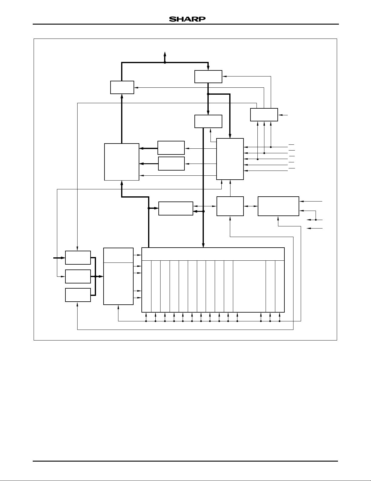
Figure 3. Flash Memory Block Diagram
Data Sheet 7

LRS1338A Stacked Chip (8M Flash & 2M SRAM)
Table 4. Flash Pin Descriptions
SYMBOL TYPE NAME AND FUNCTION
A
0
- A
18
Input
ADDRESS INPUTS: Inputs for addresses during read and write operations.
Addresses are internally latched during the write cycle.
DATA INPUT/OUTPUTS: Inputs da ta an d co mman ds du ring C UI wr ite cycl es ; ou t-
I/O
- I/O
0
15
Input/Output
puts data during memory array, status register, and identifier code read cycles. Data
pins float to HIG H- imp edan ce wh en the chi p is dese le ct ed or ou tp uts a r e di sabl e d.
Data is internally la tc he d dur in g a writ e cycle .
CHIP ENABLE: Activates the device’s control logic, input buffers, decoders, and
CE
Input
sense amplifiers. CE-HIGH deselects the device and reduces power consumption
to standby levels.
RESET/DEEP POWER-DOWN: Puts the device in deep power-down mode and
RP
Input
resets internal automation. RP
LOW, RP
inhibits write operations which provides data protection during power
transitions. Exit from deep power-down sets the device to read array mode. With
RP
= VHH, block erase or word write can operate to all blocks without WP state.
Block erase or word write with V
-HIGH enables normal operation. When driven
IH
not be attempted.
OE
WE
WP
Input OUTPUT ENABLE: Gates the device’s outputs during a read cycle.
Input
Input
WRITE ENABLE: Controls writes to the CIU and array blocks. Addresses and data
are latched on the rising edge of the WE
WRITE PROTECT: Master control for boot blocks locking. When V
blocks cannot be erased and programmed.
BLOCK ERASE an d WORD WRITE P OWER SUPPLY: For erasin g array bloc ks or
V
PP
Supply
writing words. With V
and word write with an invalid V
PP
≤ V
, memory contents cannot be altered. Block erase
PPLK
PP
results and should not be attempted.
DEVICE POWER SUPPLY: Do not float any power pins. With V
V
CC
Supply
write attempts to the flash memory are inhibited. Device operations at invalid
V
voltage (see ‘DC Characteristics’) produce spurious results and should not
CC
be attempted.
GND Supply GROUND: Do not float any ground pins.
< RP < VHH produce spurious results and should
pulse.
, locked boot
IL
(see ‘DC Characteristics’) produce spurious
CC
≤ V
LKO
, all
8 Data Sheet

Stacked Chip (8M Flash & 2M SRAM) LRS1338A
7
7F000
7FFFF
7EFFF
FE000
7DFFF
7D000
7CFFF
7C000
7BFFF
7B000
7AFFF
7A000
79FFF
79000
78FFF
78000
77FFF
70000
6FFFF
68000
67FFF
58000
57FFF
60000
5FFFF
50000
4FFFF
48000
47FFF
40000
3FFFF
38000
37FFF
30000
2FFFF
28000
27FFF
20000
1FFFF
18000
17FFF
10000
0FFFF
08000
07FFF
00000
8
9
10
11
12
13
14
32K-WORD MAIN BLOCK
632K-WORD MAIN BLOCK
532K-WORD MAIN BLOCK
4 32K-WORD MAIN BLOCK
332K-WORD MAIN BLOCK
232K-WORD MAIN BLOCK
132K-WORD MAIN BLOCK
032K-WORD MAIN BLOCK
54K-WORD PARAMETER BLOCK
44K-WORD PARAMETER BLOCK
34K-WORD PARAMETER BLOCK
24K-WORD PARAMETER BLOCK
14K-WORD PARAMETER BLOCK
04K-WORD PARAMETER BLOCK
14K-WORD BOOT BLOCK
0
4K-WORD BOOT BLOCK
TOP BOOT
32K-WORD MAIN BLOCK
32K-WORD MAIN BLOCK
32K-WORD MAIN BLOCK
32K-WORD MAIN BLOCK
32K-WORD MAIN BLOCK
32K-WORD MAIN BLOCK
32K-WORD MAIN BLOCK
LRS1338A-4
Principles of Operation
The LRS1388A SmartVoltage flash memory
includes an on-chip W SM to manage bloc k erase and
word write functions. It allows for: 100% TTL-level control inputs, fixed power supplies during block erasure,
word write, and minimal processor overhead with
RAM-like interface timings.
After initial device power-up or return from deep
power-down mode (see ‘Bus Operatio n’), the device
When V
altered. The CUI, with two-step bloc k erase or word
write command sequences, provides protec tion from
unwanted operations even when high voltage is
applied to V
V
is below the write lockout voltage V
CC
RP
is at VIL. The device’s boot blocks locking capability for WP
vertent code or data alteration by block erase and
word write operations.
≤ V
PP
. All write functions are d isabled when
PP
, memory contents cannot be
PPLK
provides additional protection from inad-
defaults to re ad array mode . Manipulation of external
memory control pins allow array read, standby, and
output disable operations.
Status register and identifier codes can be accessed
through the CUI indep endent of the F-V
High voltage on F-V
enables successful block era-
PP
voltage.
PP
sure and word writing. All functions associated with
altering m emory co ntents — block erase, word write,
status, and identifier codes — are accessed via the CUI
and verified through the status register.
Commands are written using standard microprocessor write timings. The CUI contents serve as input to
the WSM, which controls the block erase and word
write. The internal algorithms are regulated by the
WSM including pulse repetition , internal verif ication,
and margining of d ata. Addresses a nd data are internally latched during write cycles. Wr iting the appropriate command outputs array data, accesses the
identifier codes or outputs status register data.
Interface software that initiates and polls progress of
block erase and word write can be stored in any block.
This code is copied to and executed from system RAM
during flash memory updates. After successful completion, reads are again possible via the Read Array command. Block erase suspend allows system software to
suspend a block erase to read/write dat a from/to blocks
other than that which is suspended. Word writ e suspend allows system software to suspend a word write to
read data from any other flash memory array location.
DATA PROTECTION
Depending on the appl ication, the syst em designer
may choose to make the V
(available only when memor y block erases or word
writes are required) or hardwir ed to V
accommodates either design practice and encourages
optimization of the processor-memory interface.
Data Sheet 9
power supply switchable
PP
. The device
PPH
Figure 4. Memory Map
LKO
or when

LRS1338A Stacked Chip (8M Flash & 2M SRAM)
RESERVED FOR
FUTURE IMPLEMENTATION
DEVICE CODE
MANUFACTURER CODE
7FFFF
00001
00000
1338A-5
Bus Operation
The local CPU reads and writes f lash memory insystem. All bus cycles to or from the flash memory conform to standard microprocessor bus cycles.
READ
Information can be read from any block, identifier
codes or status register independent of the V
age. RP
can be either VIH or VHH.
The first task is to write the appropriate read mode
command (Read Array, Read Identifier Codes, or Read
Status Register) to the CUI. Upon initial device powerup or after exit from deep power-down mode, the device
automatically resets to read array mode. Five control
pins dictate the data flow in and out of the component:
CE
, OE, WE, RP and WP. CE and OE must be drive n
active to obtain data at the outputs. CE
is the device
selection control, and when active enables the selected
memory device. OE
is the data output (I/O0 - I/O15) control and when active drives the selected memory data
onto the I/O bus. WE
V
or VHH. Figure 12 illustrates a read cycle.
IH
must be at VIH and RP must be at
OUTPUT DISABLE
With OE
puts are disabled. Output pins (I/O
at a logic-HI GH le ve l ( VIH), the device out-
- I/O15) are placed
0
in a HIGH impedance state.
PP
volt-
As with any automated device, it is important to
assert RP
during system reset. When the system
comes out of reset, i t ex pec ts to re ad f ro m fl ash m emory. Automated flash memories provide status information when accessed during block erase or word write
modes. If a CPU reset occur s with no flash memory
reset, proper CPU initialization may not occur because
the flash memory may be provid ing status in formation
instead of arr ay data. SHARP ’s flash memories allow
proper CPU initialization following a system reset
through the use of RP
controlled by the same RESET
input. In this appl ication, RP is
signal that resets the
system CPU.
READ IDENTIFIER CODES OPERATION
The read identifier codes operation outputs the manufacturer code and devic e codes, the system CP U can
automatically match the device with its proper algorithms.
STANDBY
CE
at a logic HIGH level (VIH) places the device in
standby mode which substantially reduces device
power consumption. I/O
a HIGH-impedance st ate independent of OE
- I/O15 outputs are placed in
0
. If deselected during block erase or word write, the device continues functioning, and consuming active power until
the operation completes.
DEEP POWER-DOWN
RP
at VIL initiates the deep power down mode.
In read modes, RP
-LOW deselects the memory,
places output driver s in a HIGH-impedance s tate and
turns off all internal circuits. RP
a minimum of 1 00 ns. Time t
must be held LOW for
is required after
PHQV
return from power-down until initial memory access
outputs are valid. After this wake-up interval, normal
operation is restored. The CUI is reset to read array
mode and status register is set to 80H.
During block erase or word write modes, RP
-LOW
will abort the operation. Memory contents being altered
are no longer valid; the data may be partially erased or
written. Time t
HIGH (V
) before another command can be written.
IH
is required after RP goes to logic
PHWL
Figure 5. Device Identifier Code Memory Map
WRITE
Writing commands to the CUI enable reading of
device data and identifier codes. T hey also control
inspection and clearing of the status register.
When V
CC
= V
and VPP = V
CC1
, the CUI add i-
PPH
tionally controls block erasure and word write. The
Block Erase comman d requ ires ap propr iate com man d
data and an address within the block to be erased. The
Word Write command requires the command and
address of the location to be written.
The CUI does not occupy an addressable memory
location. It is wri tten wh en WE
and CE are active. The
address and data needed to execute a command ar e
latched on the rising edge of WE
or CE (whichever
goes HIGH first). Standard microprocessor write timings are used. F igure 13 a nd 14 illustrat e WE
and CE
controlled write operations.
10 Data Sheet
Stacked Chip (8M Flash & 2M SRAM) LRS1338A
COMMAND DEFINITIONS
When VPP ≤ V
, Read oper ation s from t he statu s
PPLK
Device operations are selected by writ ing specific com-
mands into the CUI. Tabl e 6 defines these comma nds.
register, identifier codes or blocks are enabled. Placing
V
on VPP enables successful block erase and word
PPH
write operations.
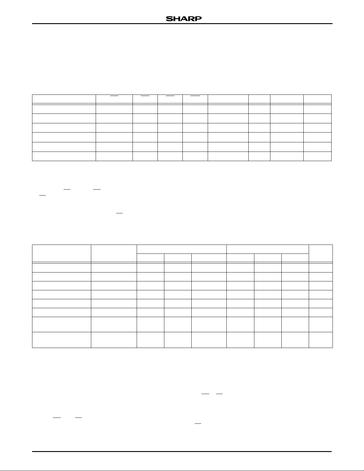
Table 5. Bus Operations
MODE RP
Read V
Output Disable V
Standby V
Deep Power-Down V
Read Identifier Codes V
Write V
NOTES:
1. Refer to ‘DC Characteristics’. When V
2. X can be V
See ‘DC Characteristics’ for V
3. Never hold OE
at GND ± 0.2 V ensures the lowest deep power-down current.
4. RP
5. See ‘Read Identifier Codes Command’ for read identifier code data.
6. Command writes involving block erase or word write are reliably executed when V
Block erase or word write with V
7. Refer to Table 6 for valid D
or VIH for control pins and addresses, and V
IL
LOW and WE LOW at the same time.
or V
IH
HH
or V
IH
HH
or V
IH
HH
IL
or V
IH
HH
or V
IH
HH
PP
and V
PPLK
< RP < VHH produce spurious results and should not be attempted.
IH
during a write operations.
IN
CE OE WE ADDRESS V
V
IL
V
IL
V
IH
V
IL
V
IH
V
IH
V
IH
XX X XHIGH Z
XXX X XHIGH Z4
≤ V
PPH
V
IL
V
IL
, memory contents can be read, but not altered.
PPLK
voltages.
V
V
PPLK
IL
IH
or V
PPH
V
IH
V
IL
for VPP.
I/O0 - I/O15NOTES
PP
XXD
OUT
1, 2, 3
XXHIGH Z
See Figure 3 X 5
XXDIN3, 6, 7
= V
PP
and VCC = V
PPH
CC1
.
1
4
OPER.2ADDR.3DATA
4
NOTES
COMMAND
Read Array/Reset
Read Identifier Codes
Table 6. Command Definitions
BUS CYCLES
REQUIRED
FIRST BUS CYCLE SECOND BUS CYCLE
OPER.
2
ADDR.
3
DATA
1 Write X FFH
2 Write X 90H Read IA ID 5
≥
Read Status Register 2 Write X 70H Read X SRD
Clear Status Register 1 Write X 50H
Block Erase 2 Write BA 20H Write BA D0H 6
Word Write 2 Write WA 40H or 10H Write WA WD 6, 7
Block Erase and Word
Write Suspend
Block Erase and Word
Write Resume
NOTES:
1. Commands other than those shown in table are reserved by SHARP for
future device implementations and should not be used.
2. BUS operations are defined in Table 5.
3. X = Any valid address within the device; IA = Identifier Code Address, see Figure 5.
BA = Address within the block being erased; WA = Address of memory location to be written.
4. SRD = Data read from status register. See Table 9 for a description of the status register bits.
WD = Data to be written at location WA. Data is latched on the rising edge of WE
ID = Data read from identifier codes.
5. Following the Read Identifier Codes command, read operations access manufacturer and device codes.
See ‘Read Identifier Codes Command’ for read identifier code data.
6. When WP
Attempts to issue a block erase or word write to a locked boot block while RP
7. Either 40H or 10H are recognized by the WSM as the word write setup.
= VIL, RP must beat VHH to enable block erase or word write operations.
1WriteXB0H 6
1WriteXD0H 6
or CE (whichever goes HIGH first).
= VIH.
Data Sheet 11
 Loading...