


®
Integrated Circuits Group
LRS1329
Stacked Chip
16M Flash and 2M SRAM
(Model No.: LRS1329)
Spec No.: MFM2-J11601
Issue Date: June 10, 1999
PRELIMINARY PRODUCT SPECIFICATIONS
SHARP
LRS1329
l
Handle this document carefully for it contains material protected by international
copyright law. Any reproduction,
full or in part,. of this material is prohibited
without the express written permission of the company.
l
When using the products covered herein, please observe.the conditions written herein
and the precautions outlined in the following paragraphs. In no event shall the
company be liable for any damages resulting from failure to strictly adhere to these
conditions and precautions.
(1) The products covered herein are designed and manufactured for the following
application areas. When using the products covered herein for the equipment
listed in Paragraph (2), even for the following application areas, be sure
to observe the precautions given in Paragraph (2). Never use the products
for the equipment listed in Paragraph (3).
*Office electronics
* Instrumentation and measuring equipment
*Machine tools
-Audiovisual equipment
*Home appliances
* Communication equipment other than for trunk lines
(2) Those contemplating using the products covered herein for the following
equipment which demands high reliability, should first contact a sales
representative of the company and then accept responsibility for incorporating
into the design fail-sale operation,
redundancy, and other appropriate measures
for ensuring reliability and safety of the equipment and the overall system.
*Control and safety devices for airplanes, trains, automobiles, and other
transportation equipment
* Mainframe computers
-Traffic control systems
. Gas leak detectors and automatic cutoff devices
*Rescue and security equipment
. Other safety devices and safety equipment,etc.
(3) Do not use the products covered herein for the following equipment which
demands extremely high performance in terms of functionality, reliability, or
accuracy.
.
* Aerospace equipment
. Communications equipment for trunk lines
*Control equipment for the nuclear power industry
-Medical equipment related to life support, etc.
(4) Please direct all queries and comments regarding the interpretation of the
above three Paragraphs to a sales representative of the company.
l
Please direct all queries regarding the products covered herein to a sales
representative of the company.
SHARP
LRS1329
1
1. Description
Contents
. . . . . . . . . . . . . . . . . . . . . . . . . . . .
2
4. Block Diagram
. . . . . . . . . . . . . . . . . . . . . . . . . .
4
5. Command Definitions for Flash Memory
- * - - * - * - - - - - * - - - - 5
8. Absolute Maximum Ratings
. . . . . . . . . . . . . . . f . . . . .
8
9. Recommended DC Operating Conditions
. . . . . . . . . . . . . . .
8
10. pi* Capacitance . - . . . . . a . . . . . a . - . a s s s s s ‘- s - e 8
11. DC Electrical Characteristics
- * - * - * * * + * - * - - * - * - *
9
12. AC Electrical Characteristics (Flash Memory) - * - * * - * * - * - * - 11
13. AC Electrical Characteristic’s (SRAM) - - * - * - - - - - - * - - - * - 18
14. Data Retention Characteristics for SRM * - * - * - - - * - - - * - - - 21
15. Notes . . . . . . . . . . . . . . . . . . . . . . . . . . . . . . . . . 22
17. Design Consideration . . . . . . . . . . . . , . . . . . . . . . . . . 24
SHARI=
LRS1329
2
Part 1 Overview
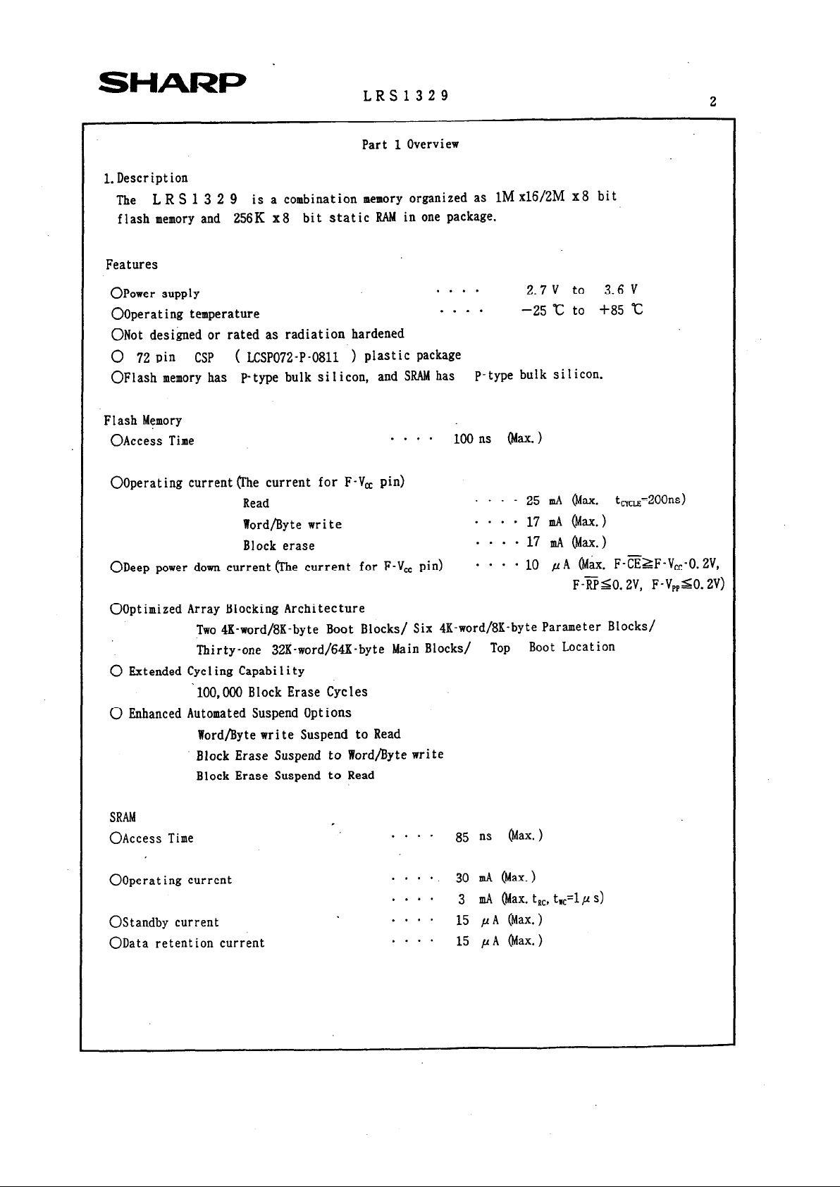
1. Description
The LR S 1 3 2 9 is a combination memory organized as lMx16/2M ~8 bit
flash memory and 256K x8 bit static RAM in one package.
Features
OPower supply
. . . .
2.7 v to 3.6 V
OOperat ing temperature
. . . .
-25 “c to +85 ‘c
ONot designed or rated as radiation hardened
0
72 pin CSP
( LCSPO72-P-0811 ) plastic package
OFlash memory has P-type bulk silicon, and SRAM has P-type bulk silicon.
Flash Memory
OAccess Time
. . . .
100 ns (Max.)
OOperating current (Ihe current for F-V, pin)
Read
Word/Byte write
Block erase
ODeep power down current (The current for F-V,, pin)
. . .
- 25 mA (Max. t,U=200ns)
. . . .
17 mA (Max.)
. . .
- 17 mA (Max.)
* * * * 10 PA (Max. F-ZZF-Vcc-0. 2V,
F-EsO. ZV, F-V&O. 2V)
OOptimized Array Blocking Architecture
Two 4X-word/8K-byte Boot Blocks/ Six 4K-word/8K-byte Parameter Blocks/
Thirty-one 32X-word/64K-byte Main Blocks/ Top Boot Location
0 Extended Cycling Capabi 1 i ty
~100,000 Block Erase Cycles
0
Enhanced Automated Suspend Options
Word/Byte write Suspend to Read
Block Erase Suspend to Nerd/Byte write
Block Erase Suspend to Read
SRAM
OAccess Time
.
OOperat ing current
OStandby current
OData retention current
. . . .
85 ns &ax. >
. . . .
30 d OhL >
. . . .
3 mA (Max. t,, t,=lp s)
. . . .
15 PA (Max.)
. . . .
15 ,uA (Max.)
SHARP
LRS1329
3
2. Pin Configuration
r INDEX
Block erase and Word/Byte Write : Vi, or V w,
Read 1 V,, or V k,,
Deep Power Down : VIL
F7@ Write Protect (Flash)
Two Boot Blocks Locked : ViL
(With F-&V m, Erase/Write can operate to all block)
F-BYTE
Byte
Enable (Flash); x8 mode: VIL, x16 mode: VI,
F-RY/BY
Ready/Busy (Flash)
During an Erase or Write operation: V,,
Block Erase and Word/Byte Write Suspend: High-Z
Deep Power Down: V,
DQ,to DQ, Data Input/Outputs (Common)
F-DQ 8 to F-DQ is Data Inputs/Outputs (Flash) ; Not used in x8 mode.
F-V,,
Power Supply (Flash)
s-“cc
Power Supply (SRAl4)
F-V,,
Write, Erase Power Supply (Flash)
Block Erase and Word/Byte Write : F-V,,=V,,,
:
Al 1 Blocks Locked 1 F-V,,<Vppll(
F-GND GND (Flash)
S-GND
GND (SRAM)
NC
No Connect
r
T, to T, Test pins (Should be open)
SHARI=
LRS1329
4
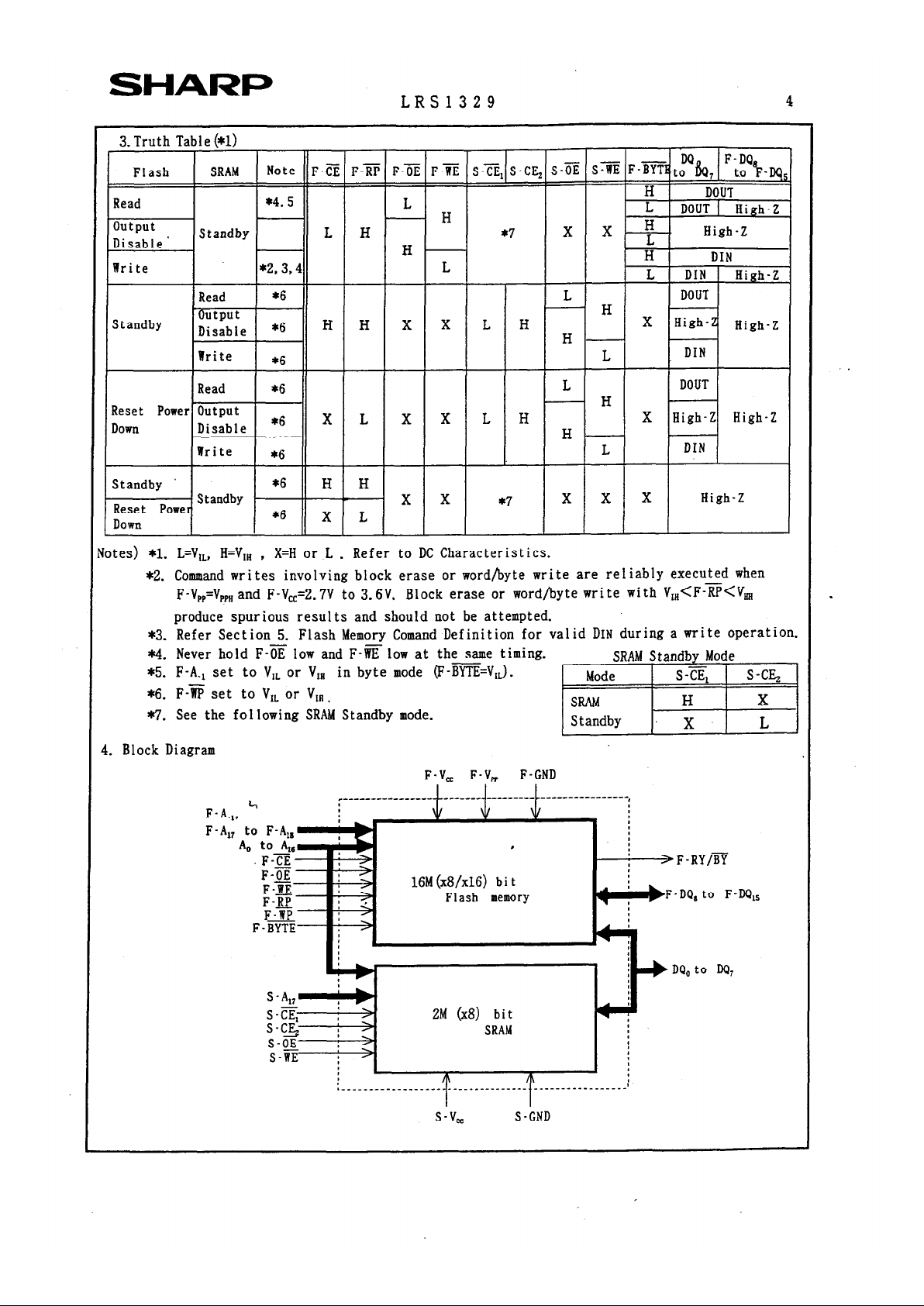
3. Truth Table (*l)
Note F-a F-B F-3 F-E S-CE, S-GE, S-s S* F-mtoDPh
F-DQ
Flash
SRAM
, to hu&
Read
*4.5
H DOUT
L
output
H
L
DOUT 1 High-Z
Disable ’
Standby L H *7
H
x x.7-.
Bigh-Z
H
L
DIN
Write
*2,3,4
L DIN High-Z
Read
*6 L
DOUT
output
H
Standby
Disable *6 H H ’ ’ L H H
X High-Z High-Z
Write
*6
L
DIN
Read *6
L
DOUT
Reset Power Output
H
Down Disable *6
XLXXLH
X High-Z Bigh-2
H -
Write
*6
L
DIN
Standby ’
*6
H H
Reset Power
Standby -
x x
*7
x x x
High-Z
Down
*6
x L
tes) *l. L=V,,, H=V,, , X=H or L . Refer to DC Characteristics.
*2. Command writes involving block erase or word/byte write are reliably executed when
F-V,,+., and F-V,=2.7V to 3-W. Block erase or word/byte write with V,,<F-B<V,
produce spurious results and should not be attempted.
*3. Refer Section 5. Flash Memory Comand Definition for valid DIN during a write operation.
*4. Never hold F-2 low and F-s low at the same timing.
-
*5. F-A., set to V,, or VI, in byte mode (F-BYTE=Vn).
*6. F-‘RP set to V,, or V,, .
*7. See the following SRAM Standby mode.
-1
Block Diagram
F-V, F-V, F-GND
----------------,
.
.F-?i? i =-
> F-RY/?%
F-X
F-E :’
16M (x8/x16) b i t
F-m +
Flash memory
F-D’& to F-W,,
F* :>
F-BYTE :T
S-A,, 4 b
S-E, I >
s-c> j >
S-OE ; >
S-IRE
2M (x8) bit
SRAM
+DQ, to W,
s-v,
S-GND
SHARP
LRS1329
5
I
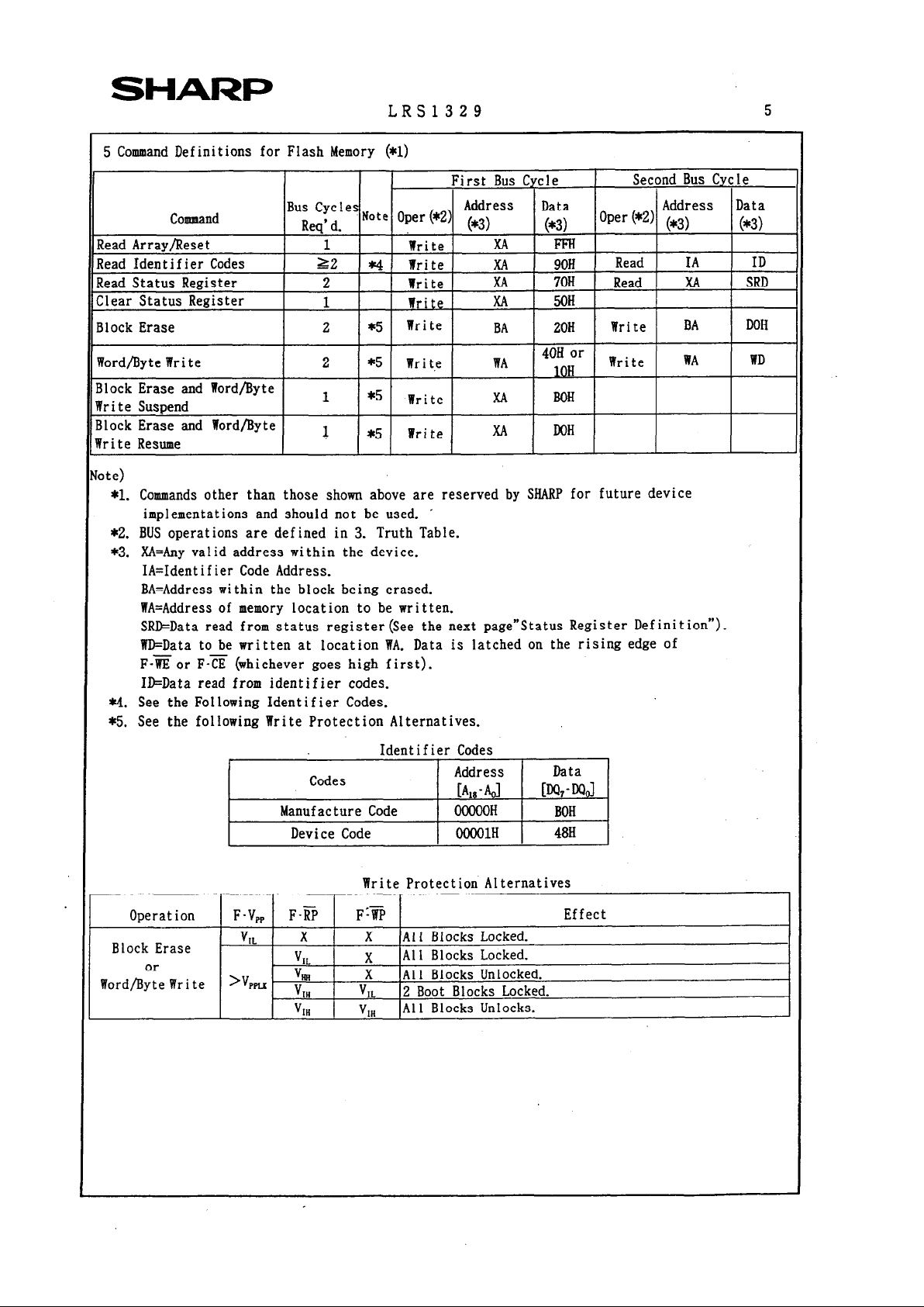
5 Command Definitions for Flash Memory (*I)
I
Word/Byte Write
Block Erase and Word/Byte
Write Suspend
Block Erase and Word/Byte
Write Resume
2 *5
Wr i t,e WA
4OH or
10H
Write WA
WD
1
*5
Write
XA Boll
XA DOH
1 *5 Write
Note)
*l. Commands other than those shown above are reserved by SHARP for future device
implementations and should not be used. ’
*2. BUS operations are defined in 3. Truth Table.
*3. XA=Any valid address within the device.
IA=Identifier Code Address.
BA=Address within the block being erased.
WA=Address of memory location to be written.
SRD=Data read from status register(See the next page”Status Register Definition”).
WD=Data to be written at location WA. Data is latched on the rising edge of
F-%?or F-5 (whichever goes high first).
II&Data read from identifier codes.
*4. See the Following Identifier Codes.
*5. See the following Write Protection Alternatives.
Write Protection Alternatives
Operation F-V,, F-i@
F?@ Effect
V
IL
X X All Blocks Locked.
Block Erase
V
X
All Blocks Locked.
or
Word/Byte Write >V,,
“t
X All Blocks Unlocked.
v
IH
V
IL
2 Boot Blocks Locked.
V
IH
V
IH
All Blocks Unlocks.
SHARP
LRS1329
6
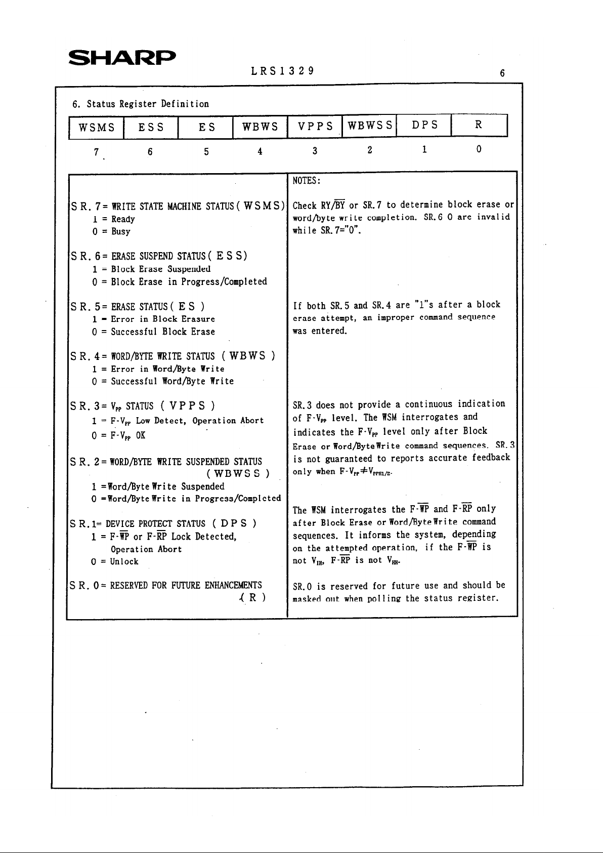
6. Status Register Definition
WSMS
ESS
ES
WBWS VPPS WBWSS
DPS R
7 6 5 4 3
2
1 0
NOTES :
S R. 7= WRITE STATE MACHINE STATUS ( W SMS) Check RYm or SR.7 to determine block erase OI
1 = Ready
word/byte write completion. SR.6-0 are invalid
0 = Busy
whi 1 e SR. 7=“0”.
SR. 6= ERASE SUSPEND STATUS( ESS)
1 = Block Erase Suspended
0 = Block Erase in Progress/Completed
SR.5=ERASESTATUS( ES )
If both SR. 5 and SR.4 are “1”s after a block
1 = Error in Block Erasure
erase attempt, an improper command sequence
0 = Successful Block Erase was entered.
S R. 4= WORD/BYTE WRITE STATUS ( WBWS )
1 = Error in Word/Byte Write
0 = Successful Word/Byte Write
SR. 3= V,, STATUS ( VPPS )
SR.3 does not provide a continuous indication
1 = F-V,, Low Detect, Operation Abort
of F-V,, level. The WSM interrogates and
0 = F-V,, OK
indicates the F-V,, level only after Block
Erase or Word/ByteWrite command sequences. SR.:
S R. 2 = WORD/BYTE WRITE SUSPENDED STATUS
is not guaranteed to reports accurate feedback
(WBWSS)
on 1 y when F-V, +Vepm,2.
1 =Word/ByteWrite Suspended
0 =Word/ByteWrite in Progress/Completed
S R . l= DEVICE PROTECT STATUS ( D P S )
1 = F-‘WP or F-@’ Lock Detected,
Operation Abort
0 = Unlock
The WSM interrogates the F-s and F-E only
after Block Erase orWord/ByteWrite command
sequences.
It informs the system, depending
on the attempted operation, if the F-w is
not VIM,
F-E is not Vm+
S R. 0 = RESERVED FOR FUTURE ENBANCEMENTS
SR.0 is reserved for future use and should be
4,R > masked out when polling the status register.
SHARP
LRS1329
7
Memory Map for Flash Memory
Address
[A,.-hl
4K*word/8K-byte Parameter Block
4K-word/BK-byte Parameter
Block
4K-word/BK-byte Parameter Block
32K-word/64K-byte Main Block
32X-word/64K-byte Main Block
323.word/64K-byte Main Block
32K-word/64K-byte Main Block
32K-word/64K.byte Main Block
32K-word/64K-byte Main Block
32K-word/64K-byte Main Block
32K-word/64K-byte Main Block
32K-word/64K-byte Main Block
32K-word/64K-byte Main Block
32K-word/64K-byte Main Block
32K-aord/64K-byte Main Block
32K-word/64K-byte tdain Block
32K-word/64K-byte Main Block
32K-word/64K-byte Main Block
32K-word/64K-byte Main Block
32K-word/64K-byte Main Block
32K-word/64K-byte Main Block
32K-word/64K-byte Main Block
32K-word/64K-byte Main Block
32K-word/64K-byte Main Block
32X-word/64K-byte Main Block
32K-word/64K-byte Main Block
32K-word/64K-byte Main Block
32K-word/64K-byte Main Block
32K-word/64K-byte Main Block
32K-word/64K-byte Main Block
32K-word/64K-byte Main Block
32K-word/64K-byte Main Block
32K-word/64K-byte Main Block
I ~~~
32K-word/64K-byte Main Block
I
19 18 17 ..... 2 1 0 20 19 18 .....
2 1 0
MSB
LSB YSB
LSB
X8
Mode
X16
Mode
I

SHARP
LRS1329
I?
8.Absolute Maximum Ratings
Parameter
Symbo 1
* Supply voltage (*l, 2)
V
cc
Ratings
-0.2 to +4.6
Unit
V
Input voltage (*l, 3)
V
IN
-0.2 (*4) to vcc+o.3
V
Operating temperature
T
OPT
-25 to +85
‘c .
Storage temperature
T,
F-;pr
-65
to +125
c
F-V,, voltage (*l)
-0.2 (*4) to +14.0(*5) V
F-E voltage (*l)
F-E
-0.5 04 to +14.0(*5)
V
Notes) *l. The maximum applicable voltage on any pins with respect to
CND.
*2. Except F-V,,.
*3. Except F-E.
*4.
-2.OV undershoot is allowed when the pulse width is less than 20nsec.
*5. i-14.OV overshoot is allowed when the pulse width is less than 20nsec.
9.Recommended DC Operating Conditions
(T,= -25 “c to +85 “c )
Parameter Symbo 1 Min.
TYP.
Max.
Unit
Supply voltage
v,
2.7 3.0
3.6
V
Input voltage
V
III
2.2
v,+o. 3(*1) v
V
IL
-0.2 (*2)
0.8
V
v, (*3)
11.4
12.6
V
Notes) *1. V, is the lower one of S-V,, and F-V, _
*2. -2.OV undershoot is allowed when the pulse width is less than 20nsec.
*3. This voltage is applicable to F-B Pin only.
10. Pin Capacitance
Parameter Symbo 1 Condition
Input capacitance Crw
vIN=ov
I/O capac i tance C
I/o
VI/o=oV
Note) *1 Sampled but not 100% Jested
(T,=25r, f=lMHz)
Min. TYP. kx.
Unit
20 pF *I
22 pF *l

SHARI=
LRS1329
9
11. DC Characteristics
Character
istics (T.= -25 “r: to +85
c
, V,= 2.7V to 3.6V)
G#pJy
F-V,
Parameter
Input leakage current (Iti)
)utput’ leakage current (IJ
V, Standby Current
T-V
PI
S-V,
Deep Power-Down Current
V,
Read Current
J,, Word/Byte Write Current
V,
Block Erase Current
J, Word/Byte Write Block
!rase Suspend Current
VP,
St andby or
Read Current
V, Deep Power-Down
Current
fpp Word/Byte Write Curren
VP,
Block Erase ‘Current
I,, Word/Byte Write or
slack Erase Suspend
Zurrent
Standby Current
Operation Current
Symbo 1
I
LX
Ll
bcs
(*2,7)
bCD (*7)
I
cm
I,,,
I
PPS
I
PPP
I
PPD
I
PW
I
PPE
I
PPIS
I
PPES
I
SB
ISBl
I
cc1
I
cc2
Conditions
V,,
=V, or CND
VOIR
=V, or GND
F-E=F-3=F-V, fO.2V
F--%F-V, fO.2V
or F-CNDfO. 2V
F -z=F -@=V,,
F-%‘=V,, or VIL
:-%=F-CNDfO. 2V,
LOUT (F-RY~bC-mA
MOS Input
:-Cj?=F-GND, f=5Mlz. I,,, =OmA
TL Input
%=F-GND, f=SMBz, Iom =omA
F-V, =vpp,
F-Vpp =vpp”
F -CE=V,,
F-V,, = F-V,,
F-V, > F-V,,
F-@=F-GNDfO. 2V
F-V, =v,,,
F - ‘4, =VPPII
F-V, =V,,,
.
S-CE,, s-cE.&s-v,-0.2v
or S-CE,IO. 2V
S -CE,=V,a or S - CEa=ViL
s -CE,=V,,,
t
,,=Min.
s - C&=V,,
II/O=omA
VIN=VI~ or V,II
s -CE,=o. 2v,
t
cYa.B=~ P s
s-C&=S-vcc-0.2v Im--om
VIN=S-vCC-O. 2V
or 0.2V
-1.5
+1.5 pA
25
50 PA
0.2 2mA
I
I I I4mA
I I
I I
I I I6b
I
I I
I
,I I lo1 2ool pA
I
I
I I
15
pA
3.0 DlA
3o DlA
I I I 31*
I
I I I

SHARP
LRS1329
10
DC Characteristics
(Continue)
-25’c to +ss”c
, V,=
2.7 V to 3.6v)
Notes)
1. Reference values at V,=3.OV and T,=+25”C.
2. Includes F-RY/BY.
3. Automatic Power Savings (APS) for Flash Memory reduces typical I,,, to 3mA
at 2.7V V, in static operation.
4. CMOS inputs are either V, fO.2V or GNMO.2V. TTL inputs are either Vi, or Vi,.
5. Block erases and word/byte writes are inhibited when F-V,, SV,,, and not guaranteed
in the range between V,, (max) and V,, (min), and above V,, (max).
6. F-3 connection to a V, supply is allowed for a maximum cumulative period of 80 hours.
7. F-m is V&O.2V in word mode and is CWO.2V in byte mode.
F-@ is V&O.ZV or CNDztO. 2V.

SHARP
LRS1329
11
12. Flash memory AC Characteristics
AC Test Condtions
Input pulse level
0 v to 2.7 V
Input rise and fall time 5
ns
Input and Output timing Ref. level 1.35 V
~ Output load
lTTLfc, (30pF)
Read Cycle
CT,=
-25°C to +SS”c ) v,(y 2.7 to 3.6V )
Notes) *l. F-n may be delayed up to tuQ,-k,,after the falling edge of F-OEwithout impact on t,,
Write Cycle (F-E Controlled) (*2)
(T,= -25°C to +85”c
, V$ 2.7v to 3.6V)
Parameter Min. Max. Unit
Write Recovery before Read
F-V,, Hold from Valid SRD, F-RY/BTHigh Z
F-E V,,,, Hold from Valid SRD, F-RY/k@-High Z
F-w Vi, Hold from Valid SRD, F-RY/B?High
hHCL
0 ns
WL
0
ns
t9
VPH
0
ns
t9
VSL
0
ns
F-BYTE Setup to F-E Going High
F-BYTE Hold from F% Hinh
hlH
50
ns
tn 100
ns
1 I
I 1 I
I

SHARP
LRS1329
12
Write Cycle (F-z Control led) (*2)
(T,= -25°C to +85X
) V,F 2.7v to 3.6v)
Notes) *2. Read timing characteristics during block erase and word/byte write operations are th
same as during read-only operations. Refer to AC Characteristics for Read Cycle.
*3. Refer to Section 5. Flash Memory Command Definition for valid
&N
and
DIN
for block
erase or word/byte write.

LRS1329
Block Erase and Word/Byte Write Performance
(T,=
-25°C to +85 c, V,= 2.7 V to 3.6 V j
hHav2 Block Erase
32K-word Block
1.2
s
t
MPVZ
Time
64K-byte Block
4K-word Block
0.5
s
8K-byte Block
huur
Word/ByteWrite Suspend
7.5 8.6
PS
hnRz1
Latency Time to Read
hm3z2
Erase Suspend Latency Time
19.3 23.6
P’s
hlmz2
to Read
^- - --. __ - _--

SHARP
LRS1329
Flash Memory AC Characteristic Timing Chart
Read Cycle timing chart
Address
DQ
F-V,
HIGH Z
Device
Address Selection
Address Stable
L
Data Valid
F-BYTE
F-BYTE timing Waveform
Standby
Address
m
Device
Address Selection
Address Stable
Data Valid
)ATA (D/Q>
HIGH Z
(IQ,-W>
DATA @/Cl)
HIGH Z
c
t
AVPV
k
t
Pm
I
HIGH Z

SHARP
LRS1329
Write cycle timeng chart (F-E controlled)
w
Address
F-E
F-Bm
F-RY/BY
t,
( b.L
L
/
\
himlII>
hWH)
l-
( ~Wvll >
tjt
am
F-WP
F-i@
F-V,,
Notes:
*l. V,, Power -up and standby.
*2. Write block erase or word/byte write setup.
*3. Write block erase confirm or valid address and data.
*4. Automated erase or program delay.
*5. Read status register data.
*6. Write Read Array command.
*1 *2
I-l-A
, *6 ,_

SHARP
LRS1329
16
Write cycle timing chart (F-E controlled)
*1
l-V--%
A
Address
F-E
F-Z
F-E
w
F-BYTE
F-RY/BY
Notes:
*l. V,, Power-up and standby.
*2. Write block erase or word/byte write setup.
*3. Write block erase confirm or valid address and data.
*4. Automated erase or program delay.
*5. Read status register data.
%.
Wri
te Read Array command.

SHARP
LRS1329
17
Reset Operations
(T,= -25 ‘c to +85 ‘c , Vcc= 2.7V to 3.6 V )
Parameter
SW.
Min. Max.
Unit
F-E Pulse Low Time
(If F-E.is tied to Vcc, this specification is not
true 100
ns
applicable.)
F?@ Low to Reset during Block Erase or
hz
23.6 ,u s
*1,2
Write
F-V,, 2.7V to F-B High h
100
ns *3
iotes)*l. If F-B is asserted while a block erase or word/bytewrite operation is not
executing, the reset will complete with loons.
*2. A reset time, t,,.
is required from the later of F-RY/BY going High Z of
F-E going
high until outputs are valid.
*3. When the device power-up, holding F-3 low minimum 1oOns is required after Vcc has
been in predefined range and also has been in stable there.
AC
Waveform for Reset Oneration
High Z
FRY/BY @) voL
V
III
F -@ (P)
VI, -
\ /
( )
t,m
(A)Reset During Read Array Mode
High Z
F-RY/BY(R)
V
OL
V
III
F-B (P)
V
IL
7
I( tpu.2 >
r I( >
t,LPil
(B)Reset During Block Erase or Word/Byte Write
.
F-i@(P)
(C)F-E Rising Timing

SHARP
LRS1329 18
13. SRAM AC Electrical Characteristics
SRAM AC Test Conditions
Input pulse level
I
0.4 v to 2.2 v
Input rise and fall time 5 ns
Input and Output timing Ref.level
1.5 V
1 Output load llTLtC, (30pF) (*l)
Note) *l. Including scope and jig capacitance.
Read Cycle
(T,= -25 =C to +85 ‘c
, v,= 2.7Vto3.6 V)
Parameter
Read Cycle Time
Address access time
Chip enable access time(S-E)
Sym. Min. Max. Unit .
hc
85
ns
hA
85
ns
hcE1
85
ns
(s-c&J
hca
85
ns
*2
*2
*2
*2
*2
*2
Write Cycle
(T,= -25 “c to +85 C
, v,=2.7 V to 3.6 V )
S-z High to output active
t
01
5
ns
*2
S-B Low to output in High impedance t, 0 25 ns
*2
L
*2. Active output to High impedance and High impedance to output active tests
specified for a f20OmV transition from steady state levels into the test load.

SHARP
LRS1329
19
SRAM AC Charaterestics Timing Chart
Read cycle timing chart- (*3)
Address
s -CE,
S-C&
S-X
D
OOI
*3 S%? is high for Read cycle.
Write cycle timing chart- (S-E Controlled)
Address
S-OE
S-CE,
S-CE,
D
OUT
D
IN
<
tic
>
Jf
‘(
t ’
OIL?
I
(*I <
tow
>
\\\\\\\\\\\\\\
(*lo)
trn
,, km
/'
(*8)
/
\
Data Valid

SHARI=
LRS1329
20
Write cycle timing chart-(S-aLow fixed)
Address
Dwr
/ / /
, , ,
, ,
I I I
I
I,
<
ta ./
tm
I-
/‘A
(*s)
DIN
/
Data Valid
Notes)
*4. A write occurs during the overlap of a low SE,, a high S-C& and a low S-x,
A write begins at the latest transition among S-m going low, S-CE,going
high and S-mgoing low.
A write ends at the earliest transition among S-z, going high, S-CE, going low
and S-E going high. twis measured from the beginning of write to the end of write.
*5.
tcr is measured from the later of S-going low or S-C& going high
to the end of write.
.
*6.
tAs is measured from the address valid to the beginning of write.
*7. tm is measured from the end of write to the address change.
a.
During this period, W pins are in the output state, therefore the input
signals of opposite phase to the outputs must not be applied.
*9. If S-E, goes low or S-C& goes high simultaneously with S-E going low or after
S-WE going low, the outputs remain in high impedance state.
*10. If S-XI goes high or S-C& goes low simultaneously with S% going high or
S-E going high, the outputs remain in high impedance state.

SHARP
LRS1329
21
14.SRAM Data Retention Characteristics
(T,=
-25°C to
+35”c >
Parameter
sym.
Conditions Min. Typ. (*l) Max. Unit
Data Retention
VCCDB
S-C& SO. 2V or
Supply volotage
S-CE,~V,w-O. 2v (*2>
2.0 3.6 V
Data Retention I
cccm
v,,=3v
Supply current S-C&SO. 2V or
S-E LV,,-0.2v (*2)
0.2 15 pA
Chip enable
setup time
bDR
0
ns
Chip enable
hold time
tR
5
lCS
Notes) *l. Reference value at T,=25’c, S-V,=3. OV.
*2. S-CE,ZV,-O.2V, S-CE.&V,-0.2V (S-E, control led) or S-C&SO. 2V (S-C& control led)
Data Retention timing chart (S-%Controlled)(*3)
L
Data Retention mode
.
()v --.---I -_--- -.-----s-e-
____I__.___..._ _ . . ..-.....- -_ -I-..._- -I_ . . . . . ..--.. --
Data Retention timing chart (S-CEz Control led)
-VCC
. CE,
Data Retention mode
/
.
/
2.JV
- . . . ..---.. _ . . . . ..- -i-‘ . .._. _ . . . .._ _._._-_..__._._ ._-_.--.-__-. _ .-._.... _.._ . . . . . . . . . . . . .
_..__.._ _..__ . . . . . ..-_.... _..._.._...__.._----_ . . . . . . . . . . . . . . .
CDP
,
0. 8
v ___.. _..__ .___ _ _____ _ __._. __________________.........~ _ .__.____.____.______ _ _.____. ___ ________.__._______...................... ._..___._.__......................... _ . . . . . . . . . _ . . . . . .
Note) *3. To control the data retention mode at S-z,, fix the input level of
S-C& between V,, and Vcc, -0.2V or OV or 0.2V and during the data retetion mode.

SHARP
LRS1329
22
15. Notes
This product is a stacked CSp package that a
16M(x8/x16) bit Flash Memory
and a
2M (x8) bit SWAM are assembled into.
Supply Power
Maximum difference (between F-V
,x and S-V,) of the voltage is less than 0.3V.
Power Supply and Chip Enable of Flash Memory and SRAM
S-E1 should not be LOW and S-Q should not be BIGH when F-Eis LOW
simulataneously.
.If the two memories are active together, possibly they may not operate normally by
interference noises or data collision on W bus.
Both F-V, and S-V, are needed to be applied by the recommended supply voltage at the
same time except SWAM data retention mode.
Power UP Sequence
When turping on Flash memory power supply, keep F-B LOW. After F-V,, reaches over
2.7V, keep F-a LOW for more than 100nsec.
Device Decoupling
The power supply is needed to be designed carefully because one of the SRAM and the
Flash Memory is in standby mode when the other is active. A careful decoupling of power
supplies is necessary between SWAM and Flash Memory. Note peak current caused by transition
of control signals (F-E, S-CE,, S-C&).

SHARP
LRS1329
23
16.Flash Memory Data Protection
Noises having a level exceeding the limit specified in the specification may be generated
under specific operating conditions on some systems.
Such noises, when induced onto F-W signal or power supply may be interpreted as false
commands, causing undesired memory updating.
To protect the data stored in the flash memory against unwanted overwriting, systems
operating with the flash memory should have the following write protect designs, as
appropriate:
1) Protecting data in specific block
By setting a F?? to low, only the boot block can be protected against overwriting.
Parameter and main blocks cannot be locked.
System program, etc., can be locked by storing them in the boot block.
When a high voltage is applied to F-E, overwrite operation is enabled for all blocks.
For further information on setting/resetting of block bit,and controlling of F-e and F-D,
refer to the specification. (See 5.Command Definitions P.5)
2) Data protection through Vpp
When the level of Vpp is lower than VPPLK(lockout voltage), write operation on the
flash memory is disabled.
All blacks are locked and the data in the blocks are completely
write protected.
For the lockout voltage, refer to the specification. (See Chapter 11. DC Characteristics P-10)
Data protection during voltage transition
1) Data protection thorough F-s
When the F-E is kept low during power up and power down sequence, write operation on
the flash memory is disabled, write protecting all blocks.
.
For the details of F-E control, refer to the specification. (See chapter 12. Flash Memory
AC Electrical.Characteristics)

SHARF)
LRS1329
24
17. Design Considerations
1. Power Supply Decoupling
To avoid a bad effect to the system by flash memory power switching characteristics,
each device should have a O.lpF ceramic capacitor connected between its V, and GND
and between its V,,and CND. Low inductance capacitors should be placed as close as
possible to package leads.
2. V,,Trace on Printed Circuit Boards
Updating the memory contents of flash memories that reside in the target system requires
that the printed circuit board designer pay attention to the Vr, Power Supply trace.
Use similar trace widths and layout considerations given to the Vcc power bus.
3. The Inhibition of Overwrite Operation
Please do not execute reprogramming “0” for’the bit which has already been
programed “0”. Overwrite operation may generate unerasable bit.
In case of reprogramming “0” to the data which has been programed “1”.
* Program “0” for the bit in which you want to change data from “1” to “0”.
* Program “1” for the bit which has already been programmed “0”.
For example, changing data from “1011110110111101” to “1010110110111100” requires
“1110111111111110” programming.
4. Power Supply
Block erase, full chip erase, word/byte write and lock-bit configuration with an invalid
V,,(See 11. DC Characteristics) produce spurious results and should not be attempted.
Device operations at invalid Vcc voltage(see ll.DC Characteristics) produce spurious
results and should not be attempted.
I

INDEX
TOP VIEW-,--
I
I
---e-e
0
-i-
-----a
0
I
:
0
01
6
+o
1
-- ---
----.
0
ai
1’
\
,
\ -
\
‘
\
/
i i
II
\
I
----____ 1
’ \/
I
I
1 u c-1 , ,
:\j
\
I ”
\
I
\ ,
1. 1 TYP.
=
TYP.
to
C
0. 8
,=
OJ
0. 4
TYP.
I
3
I
\/
/ I
000bOL!000OOO
\
?z
/I
”
0000~0000
a
4
---
BOTTOM VIEW
P
oooo;ooo~
I I
m
0000~0000 1
.----e-v-
1
P
0 0 0 oT~~~j-cc.----
I
”
OOOOiOOOO
m
0000~0000
I
ti
c
a,
d
v
~0000601000000
1 2 3 4 5 6,171 6 9101112
I
i=?ES SCALE
WI UNIT
slF%H
16M FLASH .yEMORYCXL6aa)
APPL t
c.4aLz
+ZM SRAM CXSI
5/l
l=l/lmm
MODEL
- SC’b’J71
-
MATRIX
LCSPO72-P-081
 Loading...