

Sharp LR38603 Datasheet
LR38603
BACK
DESCRIPTION
The LR38603 is a CMOS digital signal processor for
color CCD video camera systems of 270 k/320 k/
410 k/470 k-pixel CCDs with complementary color
filters. The video camera system consists of
CDS/PGA/ADC IC (IR3Y48A1), DSP IC (LR38603)
and V driver IC (LR36685) with CCD.
FEATURES
• Designed for 1/4-type 270 k/320 k/410 k/470 kpixel color CCDs with Mg, G, CY, and Ye
complementary color filters
• Switchable between NTSC and PAL modes
• Built-in signal generation circuit for driving CCD
and various pulses for TV signals
• Parameters for camera signal processing can be
set
• Built-in auto exposure control
• Built-in auto white balance control
• Built-in auto carrier balance control
• Built-in drive circuit for 2 K-bit EEPROM
• Built-in 9-bit D/A converter
• Built-in mirror image output
• Built-in circuit to reduce line crawl noise
• Built-in auto white detect correction
• YUV digital output (8 bits x 2)
• UYVY digital output (8 bits x 1)
• Analog video output
• External clock input (8 fsc)
• Built-in vertical reset
• Built-in horizontal reset
• Single +3.3 V power supply
• Package :
80-pin LQFP (P-LQFP080-1212) 0.5 mm pin-pitch
LR38603
Digital Signal Processor for
Color CCD Cameras
In the absence of confirmation by device specification sheets, SHARP takes no responsibility for any defects that may occur in equipment using any SHARP devices shown in
catalogs, data books, etc. Contact SHARP in order to obtain the latest device specification sheets before using any SHARP device.
1
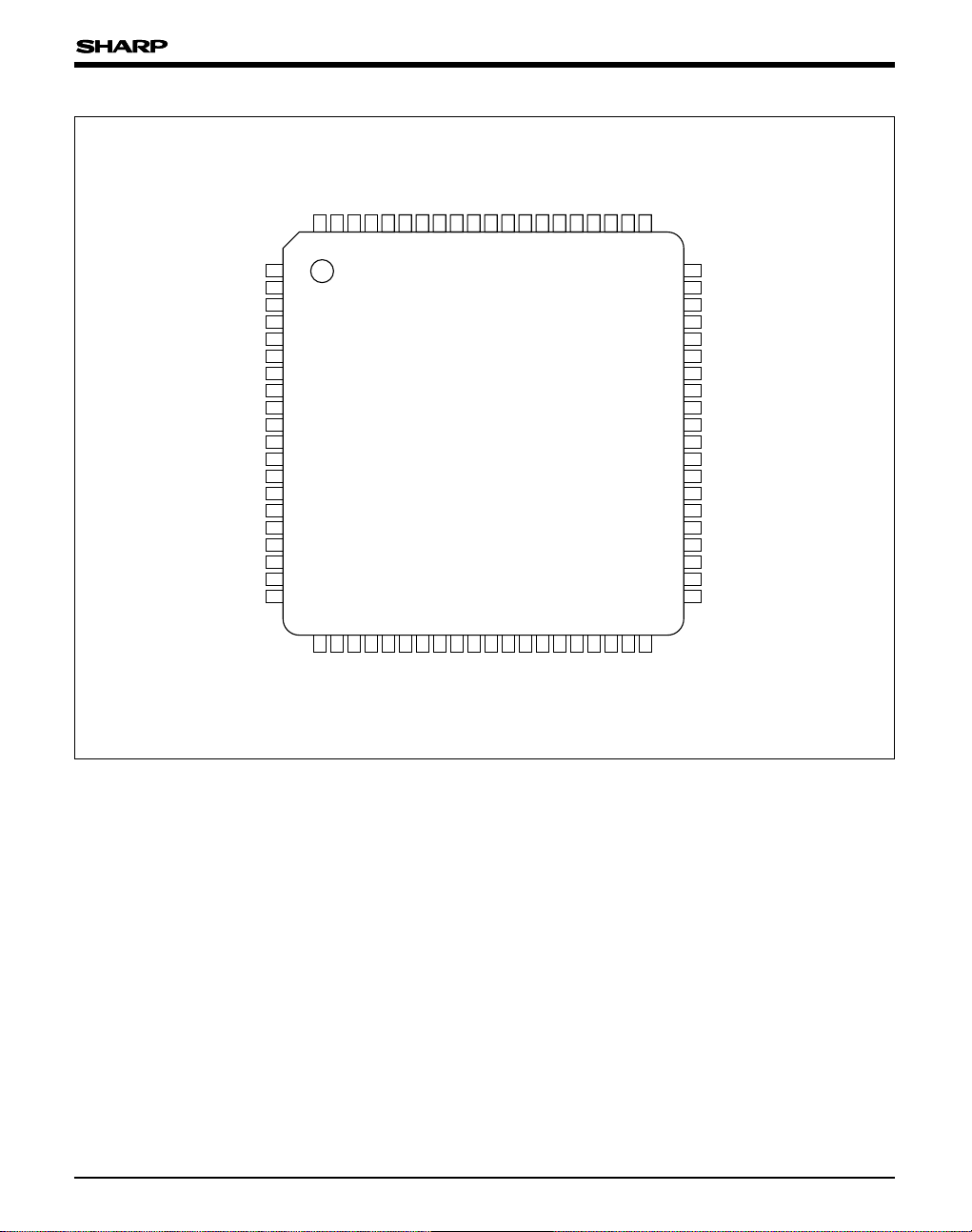
PIN CONNECTIONS
1
2
3
4
5
6
7
8
9
10
11
12
13
14
15
16
17
18
19
20
60
59
58
57
56
55
54
53
52
51
50
49
48
47
46
45
44
43
42
41
21222324252627282930313233343536373839
40
ACL
CKI
CKO
V
DD
GND
ADCK
SCK
SDATA
ADI
9
ADI8
ADI7
ADI6
ADI5
ADI4
VDD
GND
ADI
3
ADI2
ADI1
ADI0
OBCP
ADCLP
BLKX
EEPDA
GND
V
DD
EEPCK
EEPFL
EEPSL
WB
1
WB2
MIR
BLC
GNDDA
V
DDDA
VB
I
REF
VREF
GNDDA
VIDEO
HD
Y
7
Y6
Y5
Y4
VDD
GND
Y
3
Y2
Y1
Y0
EXCKI
DCK
2
DCK1
VDD
GND
EEMD
3
EEMD2
EEMD1
EEMDS
80797877767574737271706968676665646362
61
FCDSFSRS
GND
VDDFH2
FH1FRGND
VDDOFDX
VH3XVH1X
GND
VDDV4X
V3X
V2X
V1X
VD
LR38603
80-PIN LQFP
TOP VIEW
(P-LQFP080-1212)
2
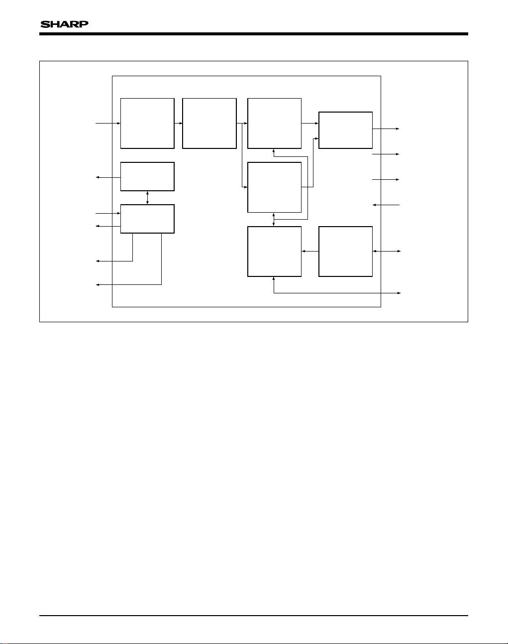
BLOCK DIAGRAM
ADI9-ADI0
VIDEO
CKI
FR, FH1, FH2
V1X-V4X
VH1X, VH3X
OB
CLAMPING
4 LINES
DELAY
LUMINANCE
SIGNAL
PROCESS
9-BIT DA
COLOR
SIGNAL
PROCESS
SSG
TG
BLKX, CSYNC
HD, VD, ADCLP
OBCP
FCDS, FS, RS
ADCK
CKO
Y7-Y0
DCK1, DCK2
EXCKI
EEPSL, EEPFL
EEPCK, EEPDA
EEMD
2, EEMD3
EEMDS, EEMD1
WB1, WB2, MIR, BLC
AUTOMATIC
CONTROL
EEPROM
CONTROL
LR38603
3
PIN DESCRIPTION
PIN NO.
SYMBOL
1 ACL ICSU All reset
2 CKI OSCI
3 CKO OSCO
DD – Power supply input (+3.3 V)
4V
5 GND – Ground
6 ADCK OBF4M
7 SCK OBF4M
8 SDATA OBF4M
9 ADI9 IC Digital signal input (MSB)
10 ADI
11 ADI
12 ADI
13 ADI
14 ADI4 IC Digital signal input
DD – Power supply input (+3.3 V)
15 V
16 GND – Ground
17 ADI
18 ADI
19 ADI1 IC Digital signal input
20 ADI
21 OBCP OBF4M
22 ADCLP OBF4M Clamp pulse output
23 BLKX OBF4M
24 EEPDA IO4MU
25 GND – Ground
DD – Power supply input (+3.3 V)
26 V
27 EEPCK IO4MSU
28 EEPFL ICU
29 EEPSL ICD
IO SYMBOL
POLARITY
Input for reference clock oscillator
Connect to CKO (pin 3) with R.
NTSC : 28.63636 MHz PAL : 28.375 MHz
Output for reference clock oscillator. The output is the inverse of CKI (pin 2).
Clock output for A/D converter
Connect to ADCK of IR3Y48A1.
Clock output for setting parameter of IR3Y48A1
Serial data output for setting parameter of IR3Y48A1
8 IC Digital signal input
7 IC Digital signal input
6 IC Digital signal input
5 IC Digital signal input
3 IC Digital signal input
2 IC Digital signal input
0 IC Digital signal input (LSB)
Clamp pulse output for optical black
Blanking pulse output
Data input from EEPROM
Connect to a data output pin of EEPROM.
When setting internal register from an external device, use EEPCK, EEPFL and
EEPSL together with EEPDA. This pin is for serial data input.
Clock output for EEPROM
Connect to clock input of EEPROM.
When setting internal register from external device, this pin is used as serial
clock.
Control for setting internal register from an external device
Usually used at H level.
Control for setting internal register from external device
Usually used at L level.
When setting register, set EEPSL at H level.
LR38603
DESCRIPTION
4
PIN NO.
SYMBOL
30 WB1 IO4MD
IO SYMBOL
POLARITY
DESCRIPTION
WB setting. Use together with WB
1 and WB2
00 (WB2, WB1) : Auto white balance 01 : WB1 mode 10 : WB2 mode
11 : WB3 mode
31 WB
2 IO4MD
These pins are 0 bit (WB
1) and 1st-bit (WB2) of UV output in output digital YUV
mode.
Setting for mirroring video output mode
32 MIR IO4MD
L : Normal H : Mirroring
This pin is 2nd-bit of UV output in output digital YUV mode.
33 BLC IO4MD
Switching internal register for exposure-standard
This pin is 3rd-bit of UV output in digital output mode.
34 GNDDA – Ground for internal D/A converter
35 V
DDDA –
Power supply for internal D/A converter
Connect to DC 3.3 V power supply (+3.3 V).
36 VB DAO DC output of internal D/A converter. Connect to ground pin via capacitor.
REF DAO DC output of internal D/A converter. Connect to ground pin via register.
37 I
REF DAI
38 V
DC reference input for internal D/A converter
Connect to DC power supply (+1.0 V).
39 GNDDA – Ground for internal D/A converter.
40 VIDEO DAO Analog video output
41 EEMDS IO4MU
42 EEMD
1 IO4MU
Switching electronic shutter control
Use together with EEMDS, EEMD
1, EEMD2 and EEMD3. Refer to "Electronic
Shutter Speed Setting" in AUTOMATIC CAMERA FUNCTION CONTROL.
These pins are 4th to 7th-bit of UV output in digital output mode.
43 EEMD
44 EEMD
2 IO4MU
3 IO4MU
When in line lock mode,
2 : H reset
EEMD
: V reset
3
EEMD
45 GND – Ground
46 V
DD – Power supply input (+3.3 V).
47 DCK
1 OBF4M
Clock output synchronized with digital output
Switchable among CSYNC, CBLK or L level.
ID pulse output of UV signal for digital output
When in analog output, output is KEI or L level.
48 DCK
2 OBF4M
KEI pulse : At power-on, begin with L level. When shutter speed is 1/60 s (PAL
1/50 s) and PGA gain is more than the value in address 92h, it goes to H level
and becomes stable.
49 EXCKI ICSU
50 Y0 OBF4M
51 Y
1 OBF4M
52 Y2 OBF4M
53 Y3 OBF4M
Input for external clock
Digital video signal output
Use together with Y
7 (MSB) to Y0 (LSB).
UYVY signal or illumination signal output (according to the register).
54 GND – Ground
LR38603
5
PIN NO.
SYMBOL
IO SYMBOL
POLARITY
DESCRIPTION
55 VDD – Power supply input (+3.3 V)
4 OBF4M
56 Y
57 Y
5 OBF4M
6
58 Y
OBF4M
59 Y7 OBF4M
Digital video signal output
Use together with Y
7 (MSB) to Y0
(LSB).
UYVY signal or illumination signal output (according to the register)
Horizontal drive pulse output
60 HD OBF4M
It is able to select horizontal drive pulse for drive timing and video output timing
from BELL pulse, HREF pulse and L level.
BELL pulse : The signal that goes to H level 1 time per 1 field.
Vertical drive pulse output
61 VD OBF4M
It is able to select from VD, CSYNC and VS outputs for drive timing and video
output timing.
1X OBF4M
62 V
63 V2X OBF4M
64 V3X OBF4M
CCD vertical drive pulse output
Connect each pin to CCD via V driver IC.
65 V4X OBF4M
66 VDD – Power supply input (+3.3 V)
67 GND – Ground
68 VH
1X OBF4M Pulse output for reading charges
Connect each pin to CCD via V driver IC.69 VH3X OBF4M
70 OFDX OBF4M OFD pulse output. Connect each pin to CCD via V driver IC.
71 VDD – Power supply input (+3.3 V)
72 GND – Ground
73 FR
74 FH1
OBF12M
OBF12M
2
OBF12M
Reset pulse output. Connect each pin to CCD via capacitor.
Horizontal transmit pulse output
Connect to CCD.75 FH
76 VDD – Power supply input (+3.3 V)
77 GND – Ground
78 RS OBF4M
79 FS OBF4M
Pulse output for sample hold
When using IR3Y48A1, connect to CSN pin for parameter setting.
Pulse output for sample hold
80 FCDS OBF4M Pulse output for sample hold
IC : Input pin
ICU : Input pin with pull-up resistor
ICD : Input pin with pull-down resistor
ICSU : Schmidt input pin with pull-up resistor
DAI : Input pin for D/A converter
OSCI : Input pin for oscillation
OBF4M : Output pin
OBF12M : Output pin
DAO : Output pin for D/A converter
OSCO : Output pin for oscillation
IO4MU : Input/output pin with pull-up resistor
IO4MD : Input/output pin with pull-down resistor
IO4MSU : Input/output pin with pull-down resistor (schmidt
input)
LR38603
6
DSP REGISTER TABLE
ADDRESS
00h
01h LPF_TH [7] H : Luminance signal processing without LPF (when using B/W CCD)
02h NI [6] 0 : Interlace 1 : Non-interlace
03h HD_SEL [6 : 5] Select output signal from HD pin
04h SW_CTRL [7 : 0] Electronic shutter control (EEMDS, EEMD
NAME BIT CONTENTS
STOP_EEPROM
[7 : 0] Stop reading from EEPROM only when EEPROM data is FF.
CCD_SEL [6 : 5] 00 : 270 k pixel CCD (NTSC) 01 : 410 k pixel CCD (NTSC)
10 : 320 k pixel CCD (PAL) 11 : 470 k pixel CCD (PAL)
ADTI [4 : 3] Input data timing adjustment
00 : Reference 01 : 1 clock delay 10 : 1 clock forward 11 : 2 clocks forward
[2] 1 : Latch with inverted clock
SEL_CDS [1 : 0] Fixed to 1X (IR3Y48A1)
MODE_OUT_SIG
Select output mode.
[5 : 3]
000 : Analog video output EXCKI : Vertical reset pulse input
001 : Analog video output EXCKI : 8 fsc clock input
2 : Horizontal reset pulse input EEMD
EEMD
010 : Analog video output EEMD
: Vertical reset pulse input
3
EEMD
2 : Horizontal reset pulse input
3 : Vertical reset pulse input
100 : YUV digital video output : Clock rate of video data pixel-CK
101 : YUV digital video output : Clock rate of video data EXCKI
110 : UYVY digital video output : Clock rate of video data EXCKI
011, 111 are prohibited.
START_EE [2] Shutter speed at power-on 0 : minimum 1 : maximum
AGC_FIX [1] PGA control 0 : Auto 1 : Fixed
OB_SEL [0] Carrier balance control 0 : Auto 1 : Fixed
00 : HD output (CCD drive timing) 01 : HD output (video output timing)
10 : BELL pulse (in analog video output), HREF (in digital video output)
11 : Fixed to L level
VD_SEL [4 : 3] Select output signal from VD pin
00 : VD output (CCD drive timing) 01 : VD output (video output timing)
10 : Fixed to L level (in analog video output), VS (in digital video output)
11 : Fixed to L level (in analog video output), CSYNC (in digital video
output)
DCK1_SEL [2 : 1] Select output signal from DCK
1 pin (in analog video output)
00 : CSYNC 01 : CBLNK 1X : Fixed to L level
DCK2_SEL [0] Select output signal from DCK
2 pin (in analog video output)
0 : Fluorescent signal 1 : Fixed to L level
1, EEME2, EEMD3), mirror video
output (MIR [MSB]), internal register for exposure-standard (BLC) and white
balance (WB
2, WB1 [LSB]) are set when selecting digital output mode with
MODE_OUT_SIG (address 02h).
Shutter control of EEMD
and that of EEMDS and EEMD
2 and EEMD3 is set by the register of SW_CTRL
1 is set by pin 41 and pin 42 when setting
"001" and "010" with MODE_OUT_SIG (address 02h).
LR38603
7
LR38603
ADDRESS
05h MIN_SH_SEL [7] Select minimum shutter speed 0 : 1/60 s (1/50 s) 1 : 1/100 s (1/120 s)
06h REF_IRIS1 [7 : 0] Reference of exposure
07h CTLD_AGC [7 : 0] Outside range of error of exposure reference
08h CTLD_0 [7 : 0] Inside range of error of exposure reference
09h REF_IRIS2 [7 : 0] Exposure reference in condition against light (When BLC = H)
0Ah CLIP_IRIS [7 : 0] Ceiling clip in accumulate exposure data
0Bh UW_E1 [7 : 0] Downward weight factor 1 in calculation of exposure. (upper of screen)
0Ch UW_E2 [7 : 0] Downward weight factor 2 in calculation of exposure.
0Dh UW_E3 [7 : 0] Downward weight factor 3 in calculation of exposure.
0Eh UW_E4 [7 : 0] Downward weight factor 4 in calculation of exposure.
0Fh UW_E5 [7 : 0] Downward weight factor 5 in calculation of exposure.
10h UW_E6 [7 : 0] Downward weight factor 6 in calculation of exposure.
11h UW_E7 [7 : 0] Downward weight factor 7 in calculation of exposure.
12h UW_E8 [7 : 0] Downward weight factor 8 in calculation of exposure. (lower of screen)
13h CW_E [6 : 0] Ratio of downward IRIS against center
14h CWP_E [5 : 0] Center point, position of left-upper area.
15h CWA_E [5 : 0] Center point, size of area.
16h EE_DIV_STP [6 : 4] Select dividing value of shutter speed control.
17h P_HEE [7 : 0] Ratio of luminance H peak of IRIS data
18h P_LEE [7 : 0] Ratio of luminance L peak of IRIS data
19h MOD8 [4] Select peak accumulation. 0 : Avg. of 8 pixels 1 : Avg. of 4 pixels
1Ah AG_DIV_STP [7 : 5] Select dividing value of PGA control.
1Bh MAX_AGC [7 : 0] Upper limitation of PGA control.
1Ch REF_AGC [7 : 0] Lower limitation of PGA control (initial value of PGA at power-on).
1Dh S_38M_GA [7 : 0] Fixed PGA gain [7 : 0 (LSB) ]
1Eh S_38M_GA_U [3] Fixed PGA gain when using IR3Y48A1 [8 (MSB)]
NAME BIT CONTENTS
MAX_SH [6 : 0] Restriction in maximum shutter speed
(When EEMDS, EEMD
(Hysteresis range of IRIS and PGA tweaking range)
(Exposure control is stopped in REF_IRIS±CTLD_0)
Sum of UW_E1 to UW_E8 must be 256d.
LPFE_O [3 : 2] Select LPF of IRIS data in PGA normal adjustment.
LPFE_I [1 : 0] Select LPF of IRIS data in PGA tweak.
IRIS_DLY [3 : 2] Reduction of IRIS control in normal operation.
00 : Operating always 01 : Operating each 2VD timing
10 : Operating each 4VD timing 11 : Operating each 8VD timing
IRIS_DLY [1 : 0] Reduction of IRIS control in PGA tweak.
00 : Operating always 01 : Operating each 2VD timing
10 : Operating each 4 VD timing 11 : Operating each 8VD timing
AG_GAIN [4 : 0] Number of steps in PGA gain
S_38M_MX
IR3Y48A1 minimum gain [1 : 0]
[2 : 0]
00 : 0 01 : +6 dB 10 : +12 dB 11 : –2 dB
1, EEMD2
, EEMD3 = 4' b1110)
8
 Loading...