Sharp LR38269 Datasheet

DESCRIPTION
The LR38269 is a CMOS digital signal processor
for color CCD camera system of 270 k/320 k-pixel
CCD with complementary color filters. The camera
system consists of CDS/AGC/ADC IC (IR3Y38M),
DSP IC (LR38269), and V driver IC (LR36685) with
CCD.
FEATURES
• Designed for 270 k/320 k color CCDs with Mg, G,
Cy, and Ye complementary color filters
• Switchable between NTSC and PAL modes
• External control interface input/output
• Variable GAMMA and KNEE response
(Select one out of 4 kinds of GAMMA & KNEE
response)
• 10-bit digital input
• Analog NTSC/PAL composite output by built-in 9bit 1 ch DA converter
• Built-in mirror image function
• Built-in timing generator to drive CCD
• Built-in 2 k-bit EEPROM controller to set the
camera adjustment data
• Built-in auto exposure control
• Built-in auto white balance control
• Built-in auto carrier balance control
• Single + 3.3 V power supply
• Package :
80-pin LQFP (LQFP080-P-1212) 0.5 mm pin-pitch
LR38269
In the absence of confirmation by device specification sheets, SHARP takes no responsibility for any defects that may occur in equipment using any SHARP devices shown in
catalogs, data books, etc. Contact SHARP in order to obtain the latest device specification sheets before using any SHARP device.
1
LR38269
Digital Signal Processor for
Color CCD Cameras
LR38269
2
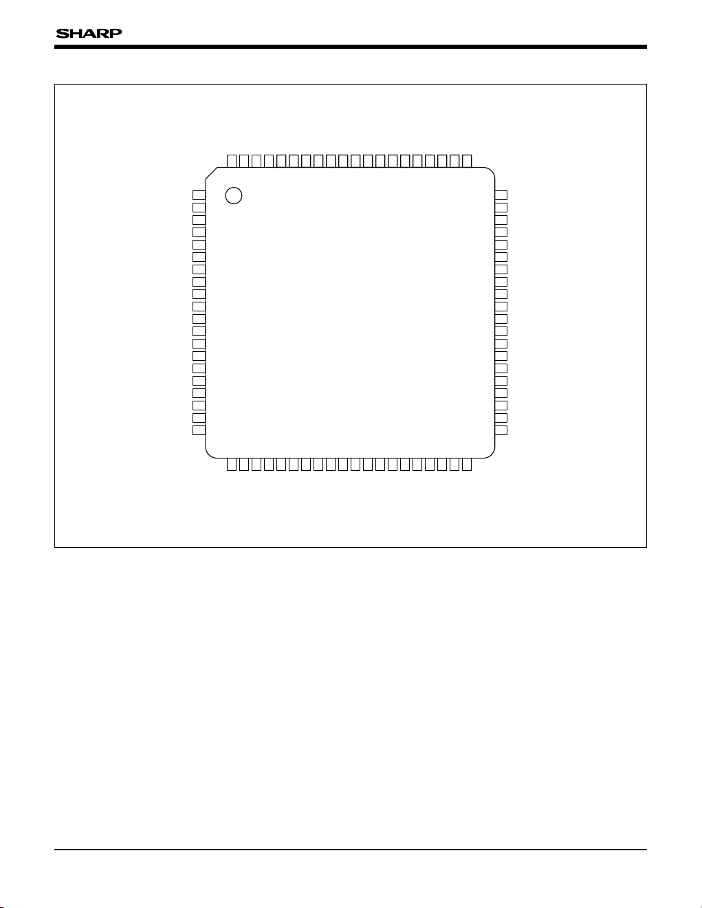
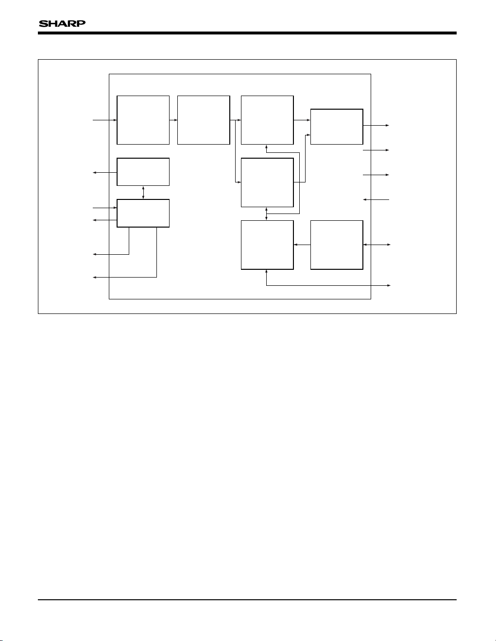
PIN CONNECTIONS
1
2
3
4
5
6
7
8
9
10
11
12
13
14
15
16
17
18
19
20
60
59
58
57
56
55
54
53
52
51
50
49
48
47
46
45
44
43
42
41
21
22
23
24
25
26
27
28
29
30
31
32
33
34
35
36
37
38
39
40
ACL
CKI
CKO
V
DD
GND
ADCK
SCK
SDATA
ADI
9
ADI
8
ADI
7
ADI
6
ADI
5
ADI
4
V
DD
GND
ADI
3
ADI
2
ADI
1
ADI
0
OBCP
ADCLP
BLKX
EEPDA
GND
V
DD
EEPCK
EEPFL
EEPSL
WB1WB
2
MIR
BLC
GNDDA
V
DDDA
V
B
I
REF
V
REF
GNDDA
VIDEO
HD
Y
7
Y6
Y5
Y4
VDD
GND
Y
3
Y2
Y1
Y0
EXCKI
DCK
2
DCK1
VDD
GND
EEMD
3
EEMD2
EEMD1
EEMDS
80
79
78
77
76
75
74
73
72
71
70
69
68
67
66
65
64
63
62
61
FCDS
FS
RS
GND
V
DD
FH
2FH1
FR
GND
V
DD
OFDX
VH
3XVH1X
GND
V
DDV4XV3XV2XV1X
VD
80-PIN LQFP
TOP VIEW
(LQFP080-P-1212)
LR38269
3
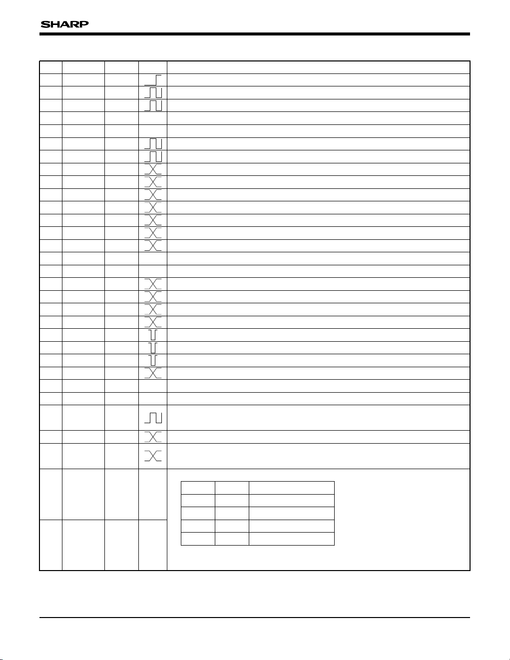
BLOCK DIAGRAM
ADI9-ADI0
VIDEO
CKI
FR, FH1, FH2
V1X-V4X
VH1X, VH3X
OB
CLAMPING
4 LINES
DELAY
LUMINANCE
SIGNAL
PROCESS
9-BIT DA
COLOR
SIGNAL
PROCESS
SSG
TG
BLKX, CSYNC
HD, VD, ADCLP
OBCP
FCDS, FS, RS
ADCK
CKO
Y7-Y0
DCK1, DCK2
EXCKI
EEPSL, EEPFL
EEPCK, EEPDA
EEMD
2, EEMD3
EEMDS, EEMD
1
WB
1, WB2, MIR, BLC
AUTOMATIC
CONTROL
EEPROM
CONTROL
LR38269
4
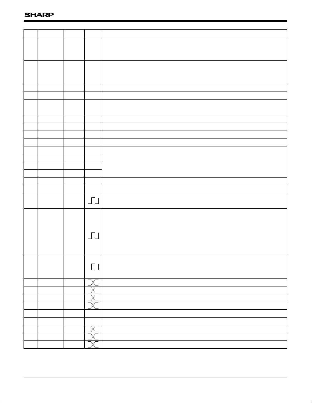
PIN DESCRIPTION
PIN NO.
SYMBOL I/O DESCRIPTION
1 ACL IC Initializing input.
2 CKI OSCI Input for reference clock oscillation. Connect to CKO (pin 3) with R.
3 CKO OSCO Output for reference clock oscillation. The output is the inverse of CKI (pin 2).
4V
DD – Supply of +3.3 V power.
5 GND – A grounding pin.
6 ADCK OBF6M Clock output of AD converter, connected to pin 13 of IR3Y38M.
7 SCK OBF4M Clock output of serial data, connected to pin 16 of IR3Y38M.
8 SDATA OBF4M Serial data output, connected to pin 19 of IR3Y38M.
9 ADI
9 IC Digital signal input, fed from pin 12 of IR3Y38M (MSB).
10 ADI8 IC Digital signal input, fed from pin 11 of IR3Y38M.
11 ADI
7 IC Digital signal input, fed from pin 10 of IR3Y38M.
12 ADI6 IC Digital signal input, fed from pin 9 of IR3Y38M.
13 ADI
5 IC Digital signal input, fed from pin 8 of IR3Y38M.
14 ADI
4 IC Digital signal input, fed from pin 5 of IR3Y38M.
15 VDD – Supply of +3.3 V power.
16 GND – A grounding pin.
17 ADI
3 IC Digital signal input, fed from pin 4 of IR3Y38M.
18 ADI
2 IC Digital signal input, fed from pin 3 of IR3Y38M.
19 ADI
1 IC Digital signal input, fed from pin 2 of IR3Y38M.
POLARITY
20 ADI0 IC Digital signal input, fed from pin 1 of IR3Y38M (LSB).
21 OBCP OBF4M
Optical clamp pulse output, connected to pin 32 of IR3Y38M.
22 ADCLP OBF4M Clamp pulse output, connected to pin 45 of IR3Y38M.
23 BLKX OBF4M
Blanking pulse output, connected to pin 35 of IR3Y38M.
24 EEPDA IO4MU
Data input from EEPROM output pin.
25 GND – Supply of +3.3 V power.
26 V
DD – A grounding pin.
27 EEPCK IO4MU
Clock output to EEPROM clock input pin.
This pin keeps high-impedance under high level of pin 29.
28 EEPFL IC
Control pin of EEPROM. Connect to the pull-up resistor.
29 EEPSL IC
Control pin of EEPROM. A pull-down resistor should be connected between pin
29 and GND. High level of pin 29 can make data-setting from outside available.
30 WB
1 IO4M
White balance mode setting by both WB1 and WB2.
In digital output mode, pin 30 is assigned to bit 0 (LSB) of U/V signal and pin 31
is assigned to bit 1.
31 WB
2 IO4M
Pin 30
0
0
1
11
0
1
0
Pin 31 White balance mode
AUTO
PRESET WB
1
PRESET WB2
PRESET WB3
LR38269
5
PIN NO.
SYMBOL I/O DESCRIPTION
POLARITY
32 MIR IO4M
Video output mode setting.
L : Normal H : Mirror
In digital output mode, this pin is assigned to bit 2 of U/V signal.
33 BLC IO4M
Backlight compensation selection.
L : OFF H : ON
In digital output mode, this pin is assigned to bit 3 of U/V signal.
34 GNDDA – A grounding pin of built-in DA converter.
35 V
DDDA – Supply of +3.3 V power of built-in DA converter.
36 V
B DAO
Bias voltage output of built-in DA converter, connected to GND through a
capacitor.
37 I
REF DAO Bias current output of built-in DA converter, connected to GND through a resistor.
38 V
REF DAI Bias voltage input of built-in DA converter, connected to +1.0 V power supply.
39 GNDDA – A grounding pin of built-in DA converter.
40 VIDEO DAO Analog video signal output.
41 EEMDS IO4MU Electronic exposure mode setting by EEMDS, EEMD1, EEMD2 and EEMD3.
See "Electronic Shutter Speed Setting" in AUTOMATIC CAMERA FUNCTION
CONTROL.
In digital output mode, 41 to 44 pins are assigned to bits 7 to 4 of U/V signals.
42 EEMD
1 IO4MU
43 EEMD
2 IO4MU
44 EEMD3 IO4MU
45 GND – A grounding pin
46 V
DD – Supply of +3.3 V power.
47 DCK
1 OBF4M
Clock output for digital signal output.
Output mode setting switches to CSYNC output.
48 DCK
2 OBF4M
ID pulse output for U/V output signal. In digital output, this pin outputs KEI-
PULSE.
NOTE : KEI-PULSE
At power-on, it keeps low. Both 1/60 s (PAL 1/50 s) as shutter speed and AGC gain
more than data of address 78h sets it high.
49 EXCKI IC
Bit 3 of address 03h sets the function of this pin.
1 : Clock input of 13.5 MHz for digital output
0 : VRI input for analog output
50 Y
0 OBF4M Bit 0 (LSB) of digital luminance signal output.
51 Y1 OBF4M Bit 1 of digital luminance signal output.
52 Y
2 OBF4M Bit 2 of digital luminance signal output.
53 Y3 OBF4M Bit 3 of digital luminance signal output.
54 GND – A grounding pin.
55 V
DD – Supply of +3.3 V power.
56 Y4 OBF4M Bit 4 of digital luminance signal output.
57 Y
5 OBF4M Bit 5 of digital luminance signal output.
58 Y6 OBF4M Bit 6 of digital luminance signal output.
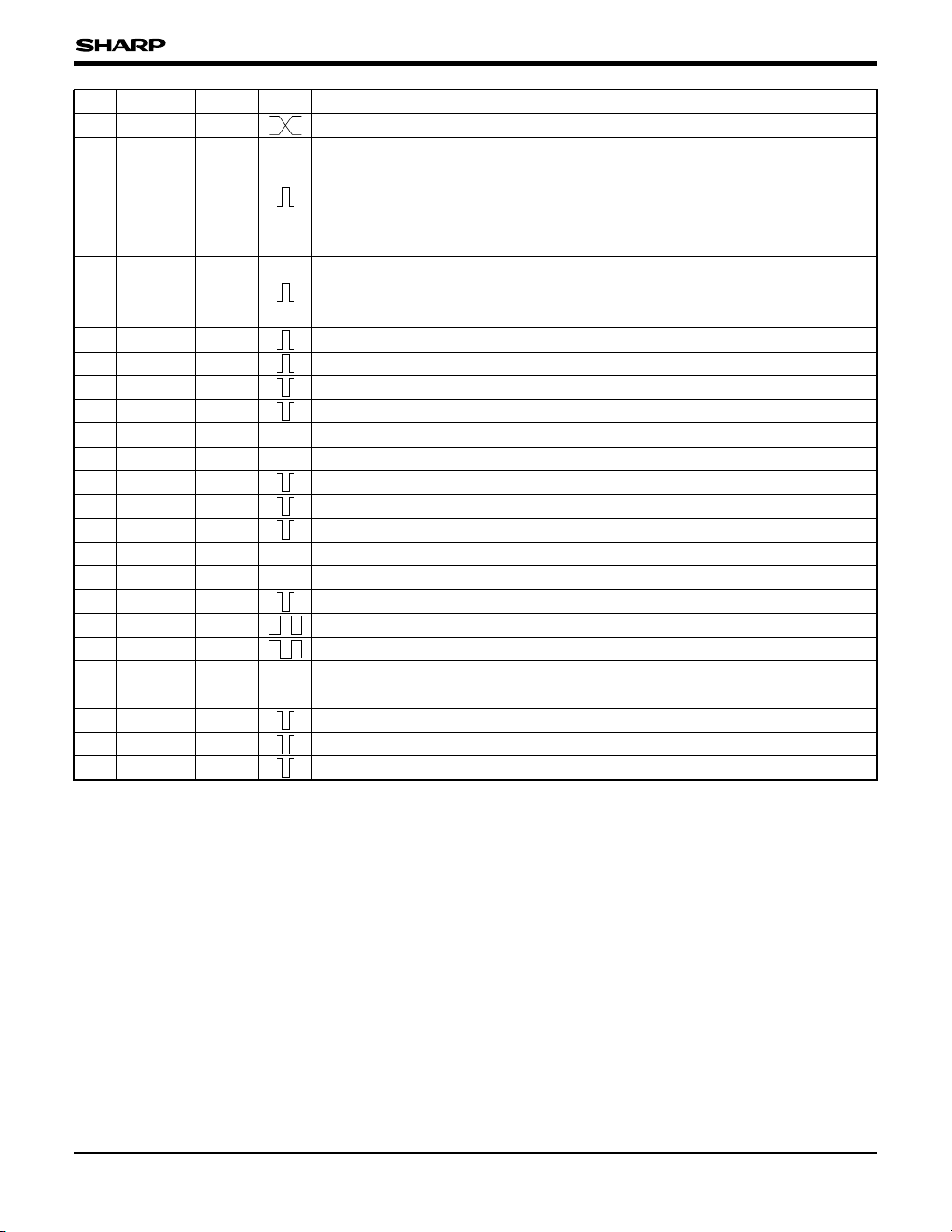
LR38269
6
IC : Input pin
OBF4M : Output pin
OBF6M : Output pin
OBF12M : Output pin
IO4M : Input/output pin
IO4MU : Input/output pin with pull-up resistor
OSCI : Input pin for oscillation
OSCO : Output pin for oscillation
DAI : Input pin for DA converter
DAO : Output pin for DA converter
PIN NO.
SYMBOL I/O DESCRIPTION
POLARITY
59 Y7 OBF4M Bit 7 (MSB) of digital luminance signal output
60 HD OBF4M
Horizontal driving pulse output. Either CCD driving timing or BELL-PULSE is
selected by output mode setting.
NOTE : BELL-PULSE
Some period with high level every field.
61 VD OBF4M
Vertical driving pulse output.
Either VD or CSYNC with either driving timing or video output timing is selected
by output mode setting.
62 V
1X OBF4M Vertical driving pulse output, connected to pin 20 of LR36685.
63 V2X OBF4M
64 V3X OBF4M
65 V4X OBF4M
66 VDD – Supply of +3.3 V power.
67 GND – A grounding pin.
68 VH
1X OBF4M Vertical driving pulse output, connected to pin 19 of LR36685.
69 VH
3X OBF4M Vertical driving pulse output, connected to pin 15 of LR36685.
70 OFDX OBF6M OFD driving pulse output, connected to pin 22 of LR36685.
71 V
DD – Supply of +3.3 V power.
72 GND – A grounding pin.
73 FR OBF12M
Reset pulse output, connected to CCD through a capacitor.
74 FH
1 OBF12M Horizontal driving pulse output, connected to CCD.
75 FH2 OBF12M Horizontal driving pulse output, connected to CCD.
76 V
DD – Supply of +3.3 V power.
77 GND – A grounding pin.
78 RS OBF6M
Sample-hold pulse output, connected to pin 31 of IR3Y38M.
79 FS OBF6M
Sample-hold pulse output, connected to pin 30 of IR3Y38M.
80 FCDS OBF6M Sample-hold pulse output, connected to both pin 28 and pin 29 of IR3Y38M.
Vertical driving pulse output, connected to pin 21 of LR36685.
Vertical driving pulse output, connected to pin 18 of LR36685.
Vertical driving pulse output, connected to pin 14 of LR36685.
 Loading...