Sharp LR38266 Datasheet

In the absence of confirmation by device specification sheets, SHARP takes no responsibility for any defects that may occur in equipment using any SHARP devices shown in
catalogs, data books, etc. Contact SHARP in order to obtain the latest device specification sheets before using any SHARP device.
1
DESCRIPTION
The LR38266 is a CMOS digital signal processor
for color CCD camera systems of 270 k/320 k/410
k/470 k-pixel CCD with complementary color filters.
FEATURES
• Designed for 270 k/320 k/410 k/470 k color CCDs
with Mg, G, Cy, and Ye complementary color
filters
• Switchable between NTSC and PAL modes
• External performance control
• Variable GAMMA and KNEE response
• 8 to 10-bit digital input
• Analog Y&C output by built-in 8-bit 2 ch DA
converter
• Switchable between Y, U/V (16 bits) and U/Y/V/Y
(8 bits) digital video output
• Line-lock and external lock function
• CPU interface input/output
• Accumulator to control auto exposure and auto
white balance
• Single +3.3 V power supply
• Package :
100-pin LQFP (LQFP100-P-1414) 0.5 mm pin-pitch
LR38266
LR38266
Digital Signal Processor for
Color CCD Cameras
LR38266
2
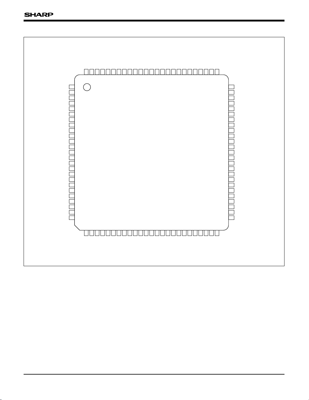
PIN CONNECTIONS
1
2
3
4
5
6
7
8
9
10
11
12
13
14
15
16
17
18
19
20
21
22
23
24
25
ACL
ADI
0
ADI1
ADI2
ADI3
ADI4
VDD
GND
ADI
5
ADI6
ADI7
ADI8
ADI9
GND
V
DD
OCP1
CSYN
GND
CKI
1
CKI2
GND
CKI
0
GND
HP
VD
75
74
73
72
71
70
69
68
67
66
65
64
63
62
61
60
59
58
57
56
55
54
53
52
51
HD1
DOC
EOO
V
DD
GND
DCK
1
YO7
YO6
YO5
YO4
GND
V
DD
YO3
YO2
YO1
YO0
VREF
DA GND
DA V
DD
IREF2
IREF1
VB2
VB1
CENCO
YENCO
26272829303132333435363738394041424344454647484950
VRI
GND
FI
CBLK
CSYO
V
DD
GND
TST
1
TST2
TST3
TST4
DCK2
GND
CO
0
CO1
CO2
CO3
GND
V
DD
CO4
CO5
CO6
CO7
TST5
TST6
100
9998979695949392919089888786858483828180797877
76
DATA7
DATA6
DATA5
DATA4
DATA3
DATA2
DATA1
DATA0
GND
VDDMCO1
ADD6
ADD5
ADD4
ADD3
ADD2
ADD1
ADD0
VDD
GND
SDI
SCK
SLDI
GND
ENC
100-PIN LQFP
TOP VIEW
(LQFP100-P-1414)
LR38266
3
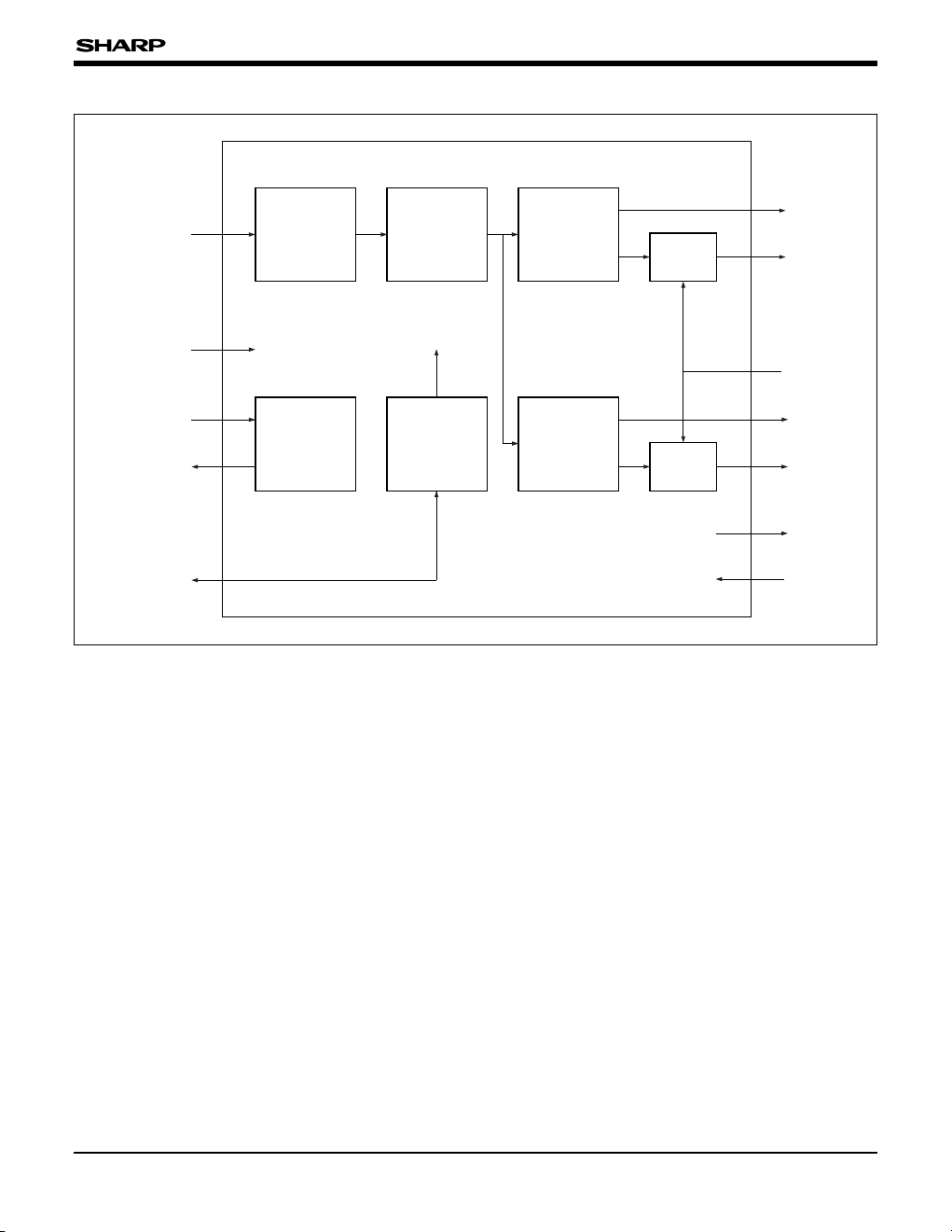
BLOCK DIAGRAM
ADI [9 : 0]
YOUT [7 : 0]
YENCO, VB
1
VREF
COUT [7 : 0]
I
REF1, IREF2
CENCO, VB2
DCK1, DCK2
DOC
ADD [6 : 0]
DATA [7 : 0]
OBCP
SSG
DAC
DAC
1H, 2H
DELAY LINE
LUMINANCE
SIGNAL
PROCESS
COLOR
SIGNAL
PROCESS
MICRO-
COMPUTER
INTERFACE
CKI
0, CKI1
HP, CSYO, HD1
CSYN, OCP1, VD, FI
CBLK, EOO, VRI
CKI
2, ENC
SDI, SCK, SLDI
4
LR38266
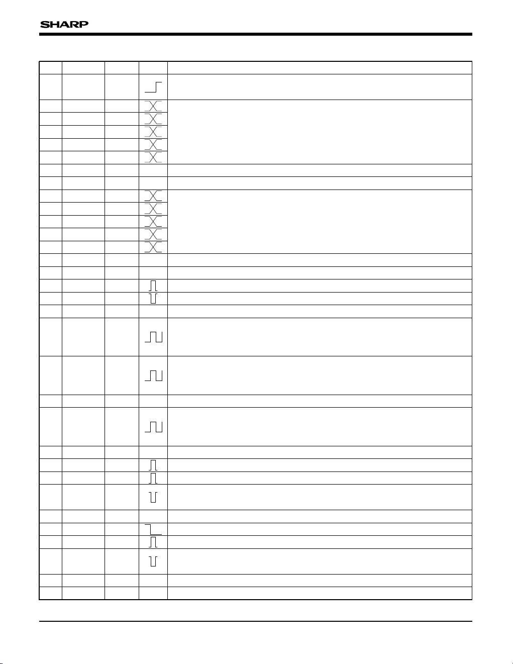
PIN DESCRIPTION
PIN NO.
SYMBOL
POLARITY
I/O DESCRIPTION
1 ACL ICU
All reset input. The internal circuit is initialized at power-on with a capacitor of
0.01 µF.
2 ADI
0 IC
ADI
0 to ADI9 are digital signal inputs.
ADI0 is LSB.
ADI
9 is MSB.
7VDD – Supply of +3.3 V power.
IC
IC
IC
IC
ADI1
ADI2
ADI3
ADI4
3
4
5
6
A grounding pin.–GND18
Composite synchronous pulse output for analog video output.OCSYNC17
Optical black clamp pulse output.OOCP116
Supply of +3.3 V power.–VDD15
A grounding pin.–GND14
ICADI913
ICADI812
ICADI711
ICADI610 ADI0 to ADI9 are digital signal inputs.
ADI0 is LSB.
ADI
9 is MSB.
ICADI
59
A grounding pin.–GND8
19 CKI
1 IC
Clock input. The frequency is below for each CCD.
270 k, 410 k CCD : 14.31818 MHz
320 k, 470 k CCD : 14.1875 MHz
Clock input. The frequency is below for each CCD.
270 k CCD : 9.5454 MHz 320 k CCD : 9.4583 MHz
410 k CCD : 14.3181 MHz 470 k CCD : 14.1875 MHz
ICCKI
220
22 CKI
0 IC
Clock input. The frequency is below for each CCD.
270 k, 410 k CCD : 28.6363 MHz
320 k, 470 k CCD : 28.3750 MHz
21 GND – A grounding pin.
23 GND – A grounding pin.
27 GND – A grounding pin.
Vertical reset input. Built-in vertical counter is reset by a low-input of more than
one horizontal period.
ICSVRI26
Vertical drive pulse output.OVD25
Horizontal drive pulse output.OHP24
Composite synchronous pulse output.
Output timing is variable by output mode.
OCSYO30
Composite blanking pulse output.OCBLK29
Supply of +3.3 V power.–V
DD31
Field index pulse output.OFI28
32 GND – A grounding pin.
5
LR38266
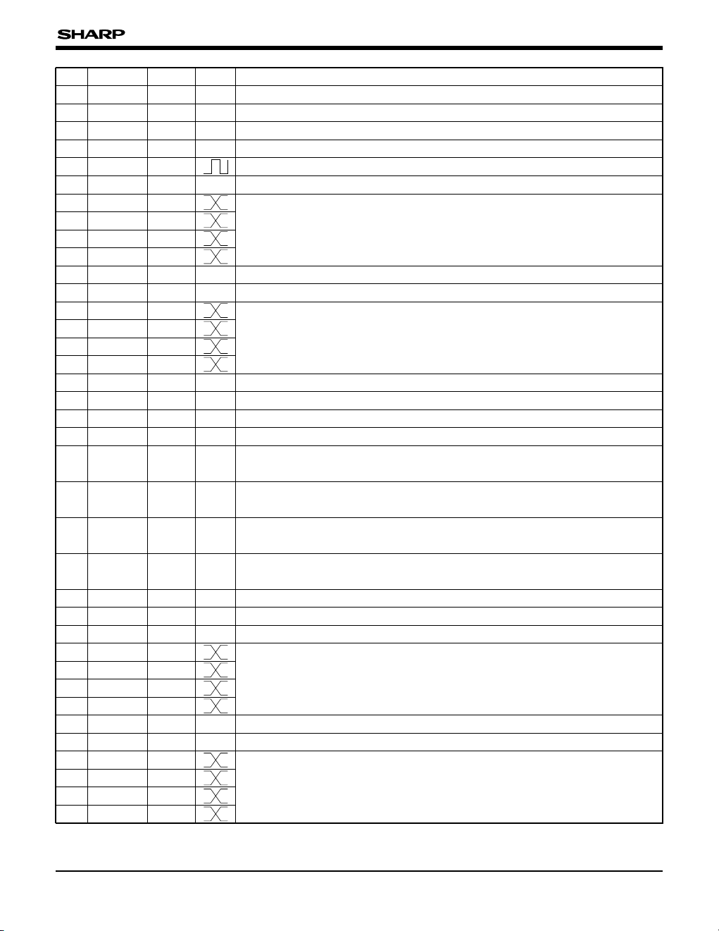
PIN NO.
SYMBOL
POLARITY
I/O DESCRIPTION
8-bit digital color signal output.
CO0 is LSB.
CO
7 is MSB.
TOCO
039
A grounding pin.–GND38
A grounding pin.–GND43
Clock output for digital COUT.ODCK237
Test input. Connected to low or open.ICDTST
436
Test input. Connected to low or open.ICDTST335
Test input. Connected to low or open.ICDTST
234
Test input. Connected to low or open.ICDTST
133
40
41
42
CO
1
CO2
CO3
TO
TO
TO
52 CENCO DAO Analog C signal output.
51 YENCO DAO Analog Y signal output.
50 TST
6 ICD Test input. Connected to low or open.
49 TST5 ICD Test input. Connected to low or open.
48 CO
7 TO
47 CO6 TO
46 CO5 TO
45 CO4 TO
8-bit digital color signal output.
CO
0 is LSB.
CO7 is MSB.
44 VDD – Supply of +3.3 V power.
Bias voltage output of built-in DA converter, connected to GND through a
capacitor.
DAOV
B254
Bias voltage output of built-in DA converter, connected to GND through a
capacitor.
DAOV
B153
57 DA V
DD – Supply of +3.3 V power input for built-in DA converter.
56 I
REF2 DAO
Bias current output of built-in DA converter, connected to GND through a
resistor.
55 I
REF1 DAO
Bias current output of built-in DA converter, connected to GND through a
resistor.
Bias voltage input of built-in DA converter, connected to +1.0 V power supply.DAIV
REF59
A grounding pin for built-in DA converter.–DA GND58
Supply of +3.3 V power.–V
DD64
Y digital outputs.
YO
0 is LSB.
YO
7 is MSB.
TOYO
060
61
62
63
YO1
YO2
YO3
TO
TO
TO
67 YO5 TO
66 YO4 TO
Y digital outputs.
YO
0 is LSB.
YO7 is MSB.
65 GND – A grounding pin.
68 YO
6 TO
TOYO769
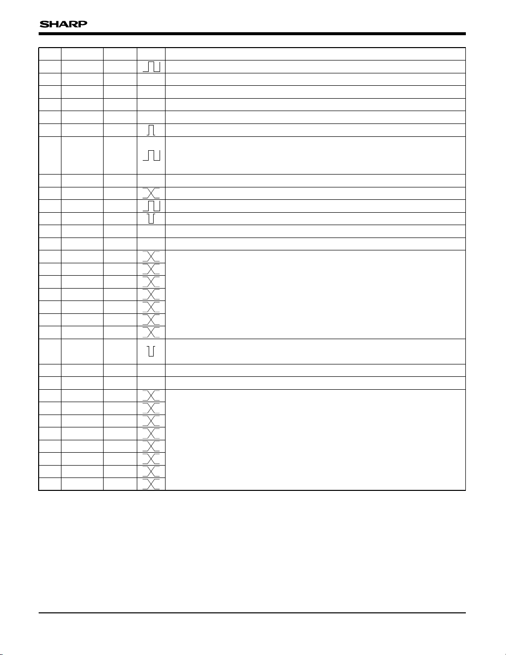
6
LR38266
PIN NO.
SYMBOL
POLARITY
I/O DESCRIPTION
Control input of YO and CO. H level sets both YO and CO high-impedance.ICDDOC74
Phase detector output comparing internal HD and HD1.XTOEOO73
Clock input to encode color signal.
Internal Synchronous mode : CKI2
Line Lock mode : same as CCD clock from outside or 4 fSC.
ICENC76
Horizontal drive pulse generated from ENC (pin 76).OHD175
A grounding pin.–GND77
Supply of +3.3 V power.–V
DD72
A grounding pin.–GND71
Clock output for YO output.ODCK170
83 ADD
0 IC
Address input to select an output data of DATA pins used in auto white
balance and auto exposure.
For details, see "Data Interface Timing".
82 VDD – Supply of +3.3 V power.
90 MCO
1 O
Control output to update internal data stored in DSP register. Data is updated
at the rising edge of MCO
1.
81 GND – A grounding pin.
80 SDI IC Timing pulse input to set SLDI data to DSP.
79 SCK IC Clock pulse input to set SLDI data to DSP.
78 SLDI IC Data input to set each coefficient of DSP.
ICADD588
ICADD487
ICADD386
ICADD285
ICADD184
89 ADD
6 IC
A grounding pin.–GND92
Supply of +3.3 V power.–VDD91
100 DATA
7 O
99 DATA6 O
98 DATA5 O
97 DATA4 O
96 DATA3 O
95 DATA2 O
94 DATA1 O
93 DATA0 O
Data output to control auto white balance and auto exposure. Data of address
set by ADD inputs is output.
For details, see "Data Interface Timing".
IC : Input pin (CMOS level)
ICU : Input pin (CMOS level with pull-up resistor)
ICD : Input pin (CMOS level with pull-down resistor)
ICS : Input pin (CMOS schmitt-trigger level with pull-
down resistor)
DAI : Input pin for DA converter
O : Output pin
TO : Tri-state output pin
XTO : Tri-state output pin
DAO : DA converter output pin
 Loading...