Sharp LQ9D161 Datasheet
‘REPARED BY: DATE SPEC No.
FILE No.
LD7620
,PPROVED BY: DATE
I
I
SHARF’
LIQUID CRYSTAL DISPLAY GROUP
SHARP CORPORATION
SPECIFICATION
f DEVICE SPECIFICATION FOR
TFT-LCDmodule
MODEL
No.
LQ9D161
ISSUE:
PACE :
APPLICABLE GROUP
Liquid Crystal Display
Group
Jun. 29. 1995
17 Rages
I
0 CUSTOMER’S APPROVAL
DATE
BY
H. FUKIJOKA’
Department General Manager
Engineering Department 2
TFf‘LCD Developmeyt Center ”
LIQUID CRYSTAL DISPLAY GROUP
SHARP CORPORATION
RECORDS OF REVISION
--. _-- -
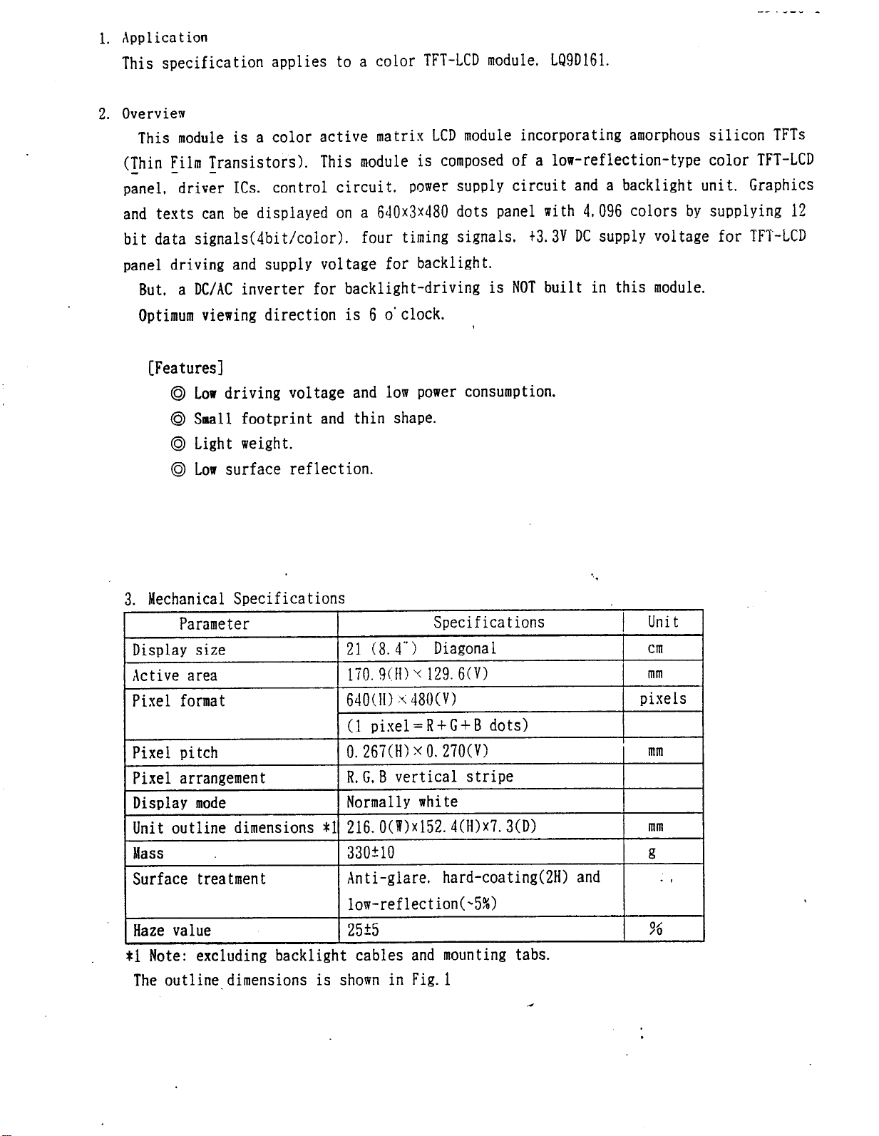
1. Application
This specification appl
ies to a color TFT-LCD module. LQ9D161.
2. Overview
This module is a color active matrix LCD module incorporating amorphous silicon TFTs
(Thin Film Transistors). This module is composed of a low-reflection-type color TFT-LCD
panel, driver ICs. control circuit.
power supply circuit and a backlight unit. Graphics
and texts can be displayed on a 640x3~480 dots panel with 4,096 colors by supplying 12
bit data signals(4bit/color). four timing signals.
t3.3V DC supply voltage for TFT-LCD
panel driving and supply voltage for backlight.
But, a DC/AC inverter for backlight-driving is NOT built in this module.
Optimum viewing direction is 6 o’clock.
[Features]
@ Low driving voltage and low power consumption.
@I Gall footprint and thin shape.
@I Light weight.
@I Low surface reflection.
3. Mechanical Specifications
Parameter
Display size
Active area
21 (8. 4”) Diagonal
170. 9(H) y 129. 6(V)
Specifications
Pixel format 640(H) .u; 480(V)
(1 pixel=R+C+B dots)
Pixel pitch
Pixel arrangement
Display mode
0.267(H) x 0.270(V)
R. G. B vertical stripe
Normally white
Unit outline dimensions *l 216.O(W)x152.4(H)x7.3(D)
Mass 3302 10
Surface treatment
Anti-glare. hard-coating(2H) and
It
Unit
cm
mm
pixels
mm
mm
g
. I
low-reflection(%5%)
Haze value 25+5
tl Note: excluding backlight cables and mounting tabs.
The outline.dimensions is shown in Fig.1
36
4. Input Terainals
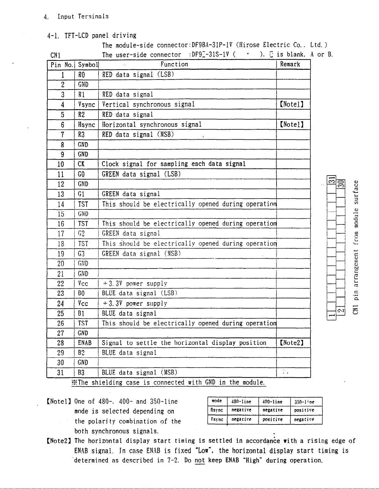
4-1. TFT-LCD panel driving
The module-side connector:DFSBA-31P-1V (Hirose Electric Co.. Ltd. >
CNl
Pin No.1 Symbolj
1
IRO
GiJD
2
3
Rl
Vsync Vertical synchronous signal
4
5 R2
Hsync Horizontal synchronous signal
6
1
7 1 R3
CND
8
GND
9
10 CK
-11 GO
12
13 Gl
14 TST
15
16
GND
GND
TST ) This should be electrically opened during operatio?
17 G2
18 )
19 t G3
1 20
1 21
TST
1 CPID 1
1 GI’JD
The user-side connector :DFSZ-31S-1V ( n 1, c is blank. A or B.
1 RED data signal (LSB)
RED data signal
RED data signal
1 RED data signal MB)
Clock signal for sampling each data signal
GREEN data signal (LSB)
GREEN data signal
This should be electrically opened during operatinr
/ GREEN data signal
/ This should be electrically opened during ope.ratio{
1 GREEN data signal (NSB)
i
22 1 vcc ( -+ 3.3V
23
I BO
24 -vcc
25
26
27
28
29 B2
30
Bl BLUE data signal
TST This should be electrically opened during operatior
GND
ENAB Signal to settle the horizontal display position
( GND 1
31 lB3
34iThe shielding case is connected with GND in the module.
/ BLUE data signal (LSBI
1 +nv poll& supply
BLUE data signal
) BLUE data signal !KB)
Function 1 Remark ’
I
(Note11
(Note11
I I
/
I I
power supply
[Note21
. ,
. [Note 1 1 One of 480-. 400- and 350-line
mnde is selected depending on
the polari tg combination of the
both synchronous signals.
(Note21 The horizontal display start timing is settled in accord&e with a rising edge of
ENAB signal. Jn case ENAB is fixed “Low”,
‘determined as described in 7-2. Do not keep ENAB “High” during operation.
-
the horizontal
display start timing is
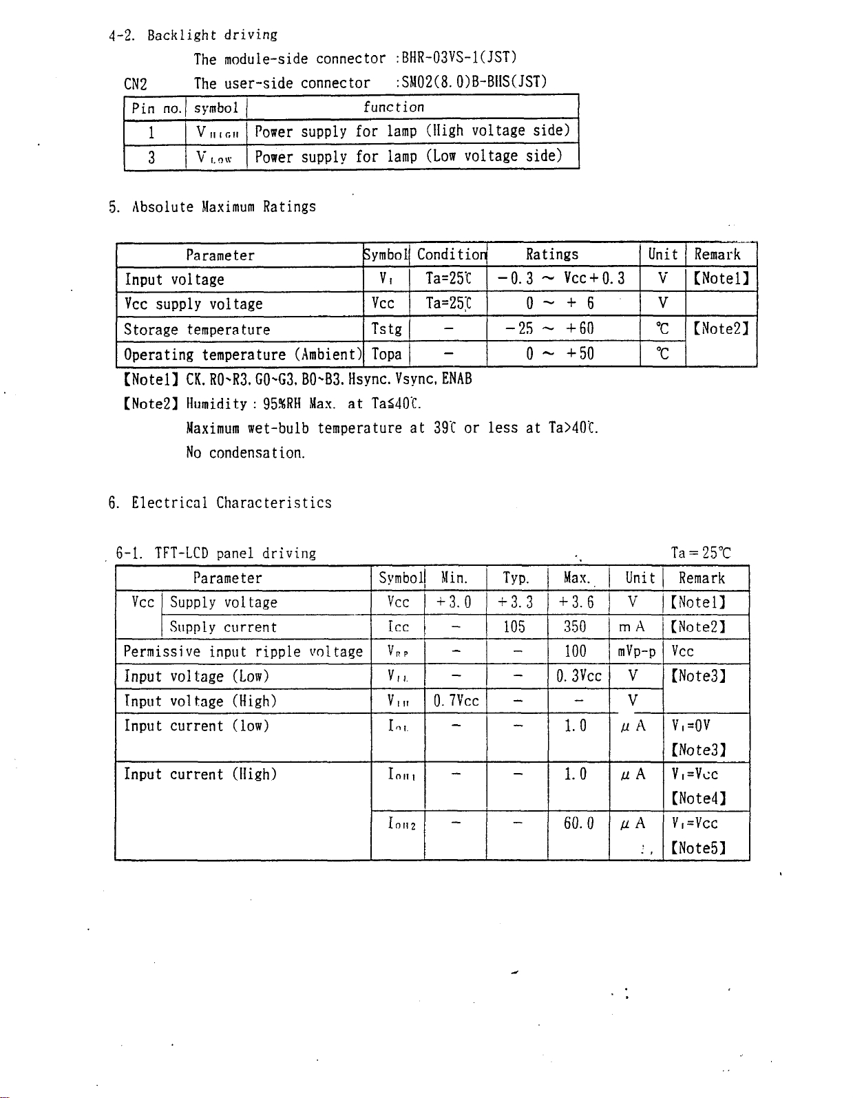
4-2. Backlight driving
The module-side connector :BHR-03Wl(JST)
CN2
Pin no. symbol 1
1 V11IGII
3
5. Absolute Maximum Ratings
(Note11 CK. ROzR3. GOG3,80~83. Hsync. Vsync, ENAB
(Note‘21 Humidity : 95%RH Max. at Tas4O’C.
The user-side connector
Power supply for lamp (High voltage side)
V C.~K Power supply for lamp (Low voltage side)
Maximum wet-bulb temperature at 39’c or less at Ta>40%.
No condensation.
:SM02(8. O>B-BIIS(JS-0
function
6. Electrical Characteristics
6-l. TFT-LCD panel driving Ta = 25°C
I
Parameter
/ vcc -:iz; 22z -
Permissive input ripple voltage
1 Input voltage (Low)
Input voltage (High)
Input current (low)
Input current (High)
Symbol( hlin.
vcc
ICC -
v
Vr,. - - 0.3vcc v
V
IO,. - - 1. 0
IO,,, / - 1 - / 1.0 / ,u A 1 ;;F=;;,
+3.0 ) +3.3 +3.6 V ) [Notell
RP
,,, 0. 7vcc - - v
1 TYP. 1 Max.. 1
105 350
- -
100
Unit 1 Remark
m A ’ (Note21
mVp-p Vcc
[Note31
fl A
v,=ov
[Note31
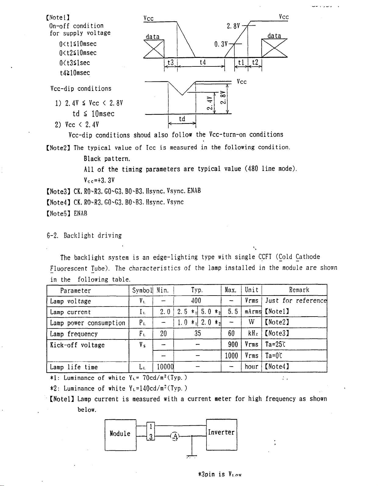
[Note11
I-?
AI”
.
On-off condition
for supply voltage
O<tlSlOmsec
0< t25 1Omsec
O( t3Slsec
t4ZlOmsec
vcc
data
vcc
vcc
Vcc-dip conditions
zz
s’
1) 2.4v S vcc < 2.8V
td 5 1Omsec
2) vcc < 2.4v
Vcc-dip conditions shoud also follow the Vcc-turn-on conditions
(Note21 The typical value of ICC is measured in the following condition.
Black pat tern.
All of the timing parameters are typical value (480 line mode).
vcc=t3.3v
(Note31 CK. RO-R3. GOG3, BO-B3. Hsync. Vsync. ENAB
43
td
-7 &
oi
s 1
(Note41 CK. RO-R3. GO-G3 BO>B3. Hsync. Vsync
(Note51 ENAB
6-2. Bach1 igh t driving
‘.
The backlight system is an edge-lighting type with single CCFT (Gold Cathode
Fluorescent Tube). The characteristics of the lamp installed in the module are shown
in the following table.
-
Lamp life time LI. 1oooc - - hour (Note41
tl: Luminance of white YL= 70cd/m’(Typ.) . I
-
1000 Vrms Ta=OC
*2: Luminance of white Y,.=140cdimz(Typ.)
(Note11 Lamp current is measured with a current meter for high frequency as shown
below.
*3pin is VI.W
 Loading...