

Page 1
Global LCD Panel Exchange Center
www.panelook.com
No. LD –21956A
DATE Oct. 6.2009
Revised
TECHNICAL LITERATURE
TFT - LCD module
MODEL No.
RoHS Compliant
FOR
LQ215M1Lxxx
The technical literature is subject to change without notice.
So, please contact Sharp or its representative before designing
your product based on this literature.
PC DISPLAY & LCD MONITOR
BUSINESS PLANNING & MARKETING PROJECT TEAM,
DIVISIONⅡ,
MOBILE LIQUID CRYSTAL DISPLAY GROUP
SHARP CORPORATION
One step solution for LCD / PDP / OLED panel application: Datasheet, inventory and accessory!
www.panelook.com
Page 2
Global LCD Panel Exchange Center
LQ215M1Lxxx
www.panelook.com
RECORDS OF REVISION
SPEC No. DATE
No. PAGE
LD-21956A Sep. 17.2009 1st Issue
REVISED
SUMMARY NOTE
One step solution for LCD / PDP / OLED panel application: Datasheet, inventory and accessory!
www.panelook.com
Page 3
Global LCD Panel Exchange Center
These technical literature sheets are the proprietary product of SHARP CORPORATION(”SHARP) and
include materials protected under copyright of SHARP. Do not reproduce or cause any third party to
reproduce them in any form or by any means, electronic or mechanical, for any purpose, in whole or in part,
without the express written permission of SHARP.
In case of using the device for applications such as control and safety equipment for transportation(aircraft,
trains, automobiles, etc. ), rescue and security equipment and various safety related equipment which require
higher reliability and safety, take into consideration that appropriate measures such as fail-safe functions and
redundant system design should be taken.
Do not use the device for equipment that requires an extreme level of reliability, such as aerospace
applications, telecommunication equipment(trunk lines), nuclear power control equipment and medical or
other equipment for life support.
www.panelook.com
LD-21956A-1
SHARP assumes no responsibility for any damage resulting from the use of the device, which does not
comply with the instructions, and the precautions specified in these technical literature sheets.
Contact and consult with a SHARP sales representative for any questions about this device.
One step solution for LCD / PDP / OLED panel application: Datasheet, inventory and accessory!
www.panelook.com
Page 4

Global LCD Panel Exchange Center
Table of contents
1. .............................................................................................................................................. 3 Application
2. ................................................................................................................................................. 3 Overview
3. ...................................................................................................................... 3 Mechanical Specifications
4. ....................................................................................................................................... 4 Input Terminals
4-1. TFT-LCD panel driving ........................................................................................................................... 4
4-2. LED Backlight driving ............................................................................................................................ 5
5. ................................................................................................................... 6 Absolute Maximum Ratings
6. ......................................................................................................................... 7 Electrical Characteristics
6-1.TFT-LCD panel driving ............................................................................................................................ 7
7. ................................................................................................ 10 Timing Characteristics of Input Signals
7-1. Timing characteristics ............................................................................................................................ 10
7-2. Input data signals and display position on the screen ............................................................................ 11
www.panelook.com
LD-21956A-2
8. ..................................................... 12 Input Signals, Basic Display Colors and Gray Scale of Each Color
9. .......................................................................................................................... 13 Optical Characteristics
10. ..................................................................................................................................... 15 Display Quality
11. ............................................................................................................................ 16 Handling Precautions
12. ......................................................................................................................................... 16 Packing form
13. ................................................................................................................................. 16 RoHS Regulations
14. ..................................................................................................................... 17 Reliability Test Condition
Fig. 1 Outline Dimensions .............................................................................................................. ……….19
One step solution for LCD / PDP / OLED panel application: Datasheet, inventory and accessory!
www.panelook.com
Page 5
Global LCD Panel Exchange Center
r
r
1. Application
This technical literature applies to a color TFT-LCD module, LQ215M1L***.
2. Overview
This module is a color active matrix LCD module incorporating amorphous silicon TFT (Thin Film
Transistor). It is composed of a color TFT-LCD panel, driver ICs, control circuit and power supply circuit
and a backlight unit. Graphics and texts can be displayed on a 1920 x 3 x 1080 dots panel with 16,777,216
www.panelook.com
LD-21956A-3
colors by using LVDS (L
voltage for TFT-LCD panel driving and supply voltage for backlight.
In this TFT-LCD panel , color filters of excellent color performance and LED backlights of high brightness
are incorporated to realize brighter and clearer pictures, making this model optimum for use in multi-media
applications.
Optimum viewing direction is 6 o'clock.
3. Mechanical Specifications
Paramete
Display size 546.86 (21.53") Diagonal mm
Active area 476.64 (H) x 268.11(V) mm
Pixel format
Aspect ratio 16 : 9
Pixel pitch 0.24825(H) x 0.24825 (V) mm
Pixel configuration R,G,B vertical stripe
ow Voltage Differential Signaling) to interface and supplying +5V DC supply
Specifications Unit
1920(H) x 1080(V) pixel
(1 pixel = R+G+B dots)
Display mode Normally white
Surface treatment Anti-glare, Haze=25%, hard-coating (3H)
Paramete
Unit outline dimensions
[Note 1]
Mass - - TBD g
[Note 1]Outline dimensions is shown in Fig.1
Min. Typ. Max. Unit
Width 495.1 495.6 496.1 mm
Height 291.7 292.2 292.7 mm
Depth 9.35 9.85 10.35 mm
One step solution for LCD / PDP / OLED panel application: Datasheet, inventory and accessory!
www.panelook.com
Page 6
Global LCD Panel Exchange Center
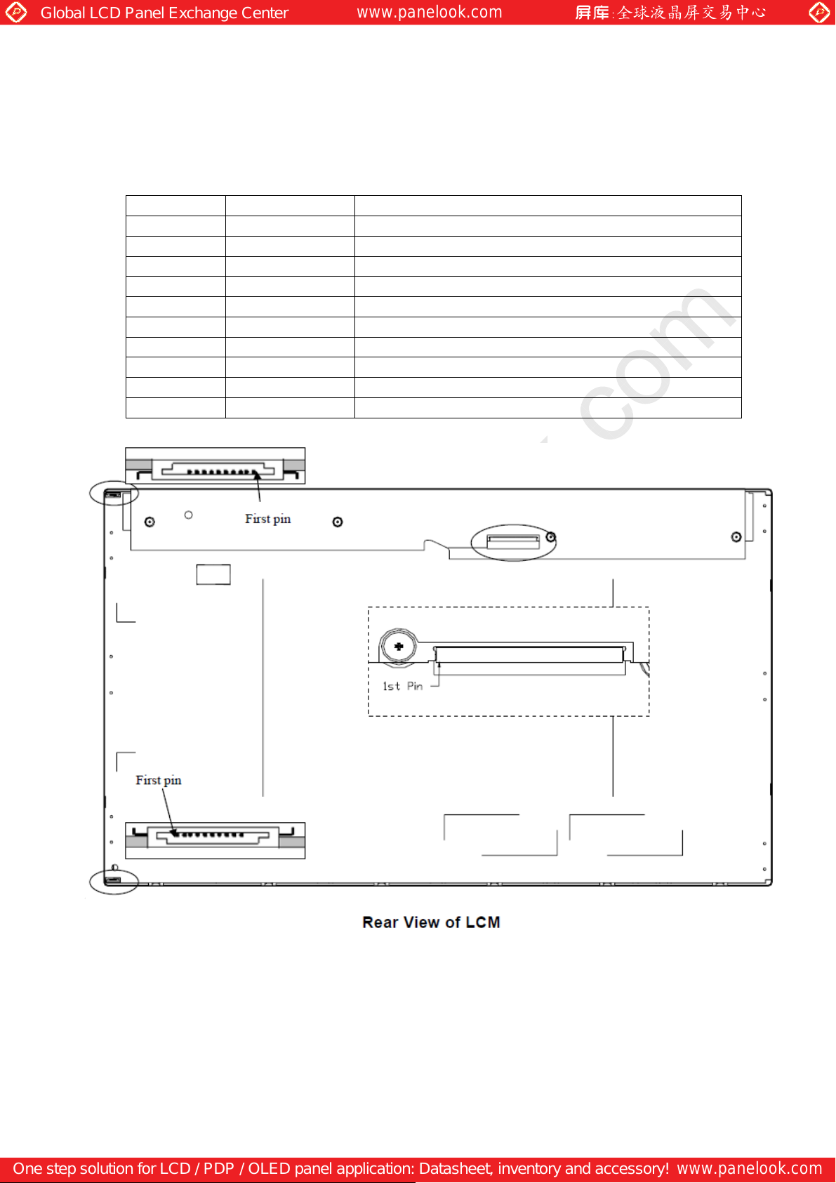
4. Input Terminals
4-1. TFT-LCD panel driving
CN1 (LVDS signals and +5.0V DC power supply)
Using connector : GS23302-0011R-7F (Foxconn) or equivalent.
Corresponding connector : FI-XB30SRL-HF11 (JAE) [Note 1]
Pin No. Symbol Function Remark
Frame
1
2
3
4
5
6
7
8
9
10
11
12
13
14
15
16
17
18
19
20
21
22
23
24
25
26
27
28
29
30
Frame
[Note 1] Sharp is not responsible to its product quality, if the user applies a connector not corresponding
GND GND
RxO0-
RxO0+
RxO1-
RxO1+
RxO2-
RxO2+
GND GND
RxOC-
RxOC+
RxO3-
RxO3+
RxE0-
RxE0+
GND
RxE1-
RxE1+
GND
RxE2-
RxE2+
RxEC-
RxEC+
RxE3-
RxE3+
GND GND
N.C. No Connection, this pin should be open.
N.C. No Connection, this pin should be open.
N.C. No Connection, this pin should be open.
Vcc +5V power supply
Vcc +5V power supply
Vcc +5V power supply
GND GND
www.panelook.com
LD-21956A-4
[Note 3]
Receiver signal of LVDS (O0-) [Note 2]
Receiver signal of LVDS (O0+) [Note 2]
Receiver signal ofLVDS (O1-) [Note 2]
Receiver signal of LVDS (O1+) [Note 2]
Receiver signal of LVDS (O2-) [Note 2]
Receiver signal of LVDS (O2+) [Note 2]
Receiver signal of LVDS CLK (OC-) [Note 2]
Receiver signal of LVDS CLK (OC+) [Note 2]
Receiver signal of LVDS (O3-) [Note 2]
Receiver signal of LVDS (O3+) [Note 2]
Receiver signal of LVDS (E0-) [Note 2]
Receiver signal of LVDS (E0+) [Note 2]
GND
Receiver signal of LVDS (E1-) [Note 2]
Receiver signal of LVDS (E1+) [Note 2]
GND
Receiver signal of LVDS (E2-) [Note 2]
Receiver signal of LVDS (E2+) [Note 2]
Receiver signal of LVDS CLK (EC-) [Note 2]
Receiver signal of LVDS CLK (EC+) [Note 2]
Receiver signal of LVDS (E3-) [Note 2]
Receiver signal of LVDS (E3+) [Note 2]
[Note 4]
[Note 4]
[Note 4]
[Note 3]
to the above model.
[Note 2] Relation between RxINi(i=0,1,2) and actual data is shown in following section (4-3).
[Note 3] The shielding case is connected with signal GND.
[Note 4] Please use NC by OPEN. NC terminal is not connected with the internal circuit.
One step solution for LCD / PDP / OLED panel application: Datasheet, inventory and accessory!
www.panelook.com
Page 7
Global LCD Panel Exchange Center
y
y
y
y
4-2. LED Backlight driving
Upper/Lower FPC Connector Pin Assignment
Using connector : 7080-Q10N-00R (Entery INDUSTRIAL CO.,LTD)
Corresponding FFC specification:
Temperature=80
www.panelook.com
o
C, Voltage=60V, Pin No.=10, 0.5Pitch, PET, HF
LD-21956A-5
Pin No Symbol
1 IRLED1 IRLED1 LED current sense for string 1
2 IRLED1 IRLED1 LED current sense for string 1
3 IRLED2 IRLED1 LED current sense for string 2
4 VLED LED power suppl
5 VLED LED power suppl
6 VLED LED power suppl
7 VLED LED power suppl
8 IRLED2 IRLED1 LED current sense for string 2
9 IRLED3 IRLED1 LED current sense for string 3
10 IRLED3 IRLED1 LED current sense for string 3
Description
One step solution for LCD / PDP / OLED panel application: Datasheet, inventory and accessory!
www.panelook.com
Page 8

Global LCD Panel Exchange Center
a
5. Absolute Maximum Ratings
www.panelook.com
LD-21956A-6
Parameter Symbol Condition
Input voltage V
Ta=25oC -0.3 +4.3 V [Note 1]
I
Ratings
Min. Max.
Unit Remark
+5V supply voltage Vcc Ta=25oC -0.3 +6.0 V
LED Driver supply voltage LED_V
Ta=25oC(TBD) (TBD) V
CC
LED Current ILED Ta=25oC(TBD) (TBD) A
Storage temperature Tstg
Operating temperature (Ambient) Top
-
-
-20 +60
0+50
o
C
o
C
[Note 3]
[Note 1] LVDS signals
[Note 2] The relative humidity must not exceed 90% non-condensing at temperatures of 40°C or less.
At temperatures greater than 40°C, the wet bulb temperature must not exceed 39°C.
One step solution for LCD / PDP / OLED panel application: Datasheet, inventory and accessory!
www.panelook.com
Page 9

Global LCD Panel Exchange Center
r
–
6. Electrical Characteristics
6-1.TFT-LCD panel driving
Ta=+25
Paramete
Symbol Min. Typ. Max. Unit Remark
Supply voltage Vcc +4.5 +5.0 +5.5 V [Note 2]
Permissive input ripple voltage VRP --150mV
Current dissipation Icc - (TBD) (TBD) mA [Note 3]
Rush Current Irush - 1.6 3.0 A [Note 4]
Input voltage range VI (TBD) (TBD) V LVDS signals
Differential input High VTH --+100mVV
threshold voltage Low VTL
Input current (High) IOH --(TBD)μAVI = +2.4V Vcc = +3.6V
Input current (Low) IOL --(TBD)μAVI = 0V Vcc = 3.6V
Terminal resistor R
[Note 1] VCM : Common mode voltage of LVDS driver.
[Note 2] On-off conditions for supply voltage
www.panelook.com
Vcc = +5.5V
P-P
= +1.2V
CM
100 - - mV [Note 1]
-(TBD)- Ω Differential input
T
LD-21956A-7
o
C
0.1Vcc
Vcc
t1 t2
Valid
0.9Vcc0.9Vcc
0.1Vcc
t3 t5
t4
0.1Vcc
Signal
(LVDS Interface)
Backlight
OFF
t6
Backlight ON
(LED)
t7
OFF
Symbol Min. Typ. Max. Unit Remark
t1 0.1 - 10 ms
t2 0 30 50 ms
t3 0 20 50 ms
t4 0.1 - 10 ms
t5 1000 - - ms
t6 200 250 - ms *1
t7 100 250 - ms *1
*1 : As for the power sequence for backlight, it is recommended to apply above
mentioned input timing. If the backlight is lit on and off at a timing other
than shown above, displaying image may get disturbed. This is due to
variation of output signal from timing generator when LVDS signal is
changed from on to off or vice versa, but has no harm to the module itself.
(Note 2-1) Do not keep the interface signal high-impedance or unusual signal when power is on.
(Note 2-2)Vcc-dip conditions
One step solution for LCD / PDP / OLED panel application: Datasheet, inventory and accessory!
www.panelook.com
Page 10

Global LCD Panel Exchange Center
www.panelook.com
LD-21956A-8
[Note 3] Typical current situation : 16-gray-bar pattern.
Vcc=+5.0V
Maximum current situation : Vcc=+5.0V
[Note 4] Test condition :
DD = 5 V, VDD rising time = 470 μs ± 10%
(1) V
(2) Pattern: Mosaic pattern
(3) Test circuit
RGB
GS0
RGB
GS4
RGB
GS8
....
RGB
GS56
RGB
GS60
[Note 5] LVDS signal definition
VIN+ = Positive differential DATA & CLK Input
VIN- = Negative differential DATA & CLK Input
VID = VIN+ – VIN- ,
ΔVCM =|VCM+–VCM-|,
ΔVID =|VID+–VID-|,
VID+ =|VIH+–VIH-|,
VID- =|VIL+–VIL-|,
VCM = (VIN+ +VIN-)/2,
VCM+ = (VIH+ +VIH-)/2,
VCM- = (VIL+ +VIL-)/2,
One step solution for LCD / PDP / OLED panel application: Datasheet, inventory and accessory!
www.panelook.com
Page 11

Global LCD Panel Exchange Center
r
6-2. Backlight driving
www.panelook.com
LD-21956A-9
(Ta=+25
o
C)
Paramete
Symbol Min. Typ. Max. Unit Remark
Supply voltage range VLED - +42.9 +45.5 V (Duty 100%)
Current dissipation ILED
-
- 360 mA [Note 1,2,3]
Power Consumption PLED 16.38 W [Note 4]
Permissive input ripple voltage -
-
-(TBD)mV
[Note 1]
P-P
LED life time LBL - 30,000 - Hour [Note 5]
[Note 1] There are one Light Bar, and the specified current is input LED chip 100% duty current.
[Note 2] The sensing current of each string is 60mA.
[Note 3] Each light bar have three current sensing strings, so that each light bar input current is 180mA.
.
[Note 4] PLED = ILED × VLED.
[Note 5] The life time is determined as the time at which luminance of the LED becomes 50% of the
initial brightness or not normal lighting at ILED=360mA on condition of continuous operating
at 25±2°C.
One step solution for LCD / PDP / OLED panel application: Datasheet, inventory and accessory!
www.panelook.com
Page 12

Global LCD Panel Exchange Center
r
y
y
7. Timing Characteristics of Input Signals
7-1. Timing characteristics
www.panelook.com
Vcc=+3.0V~+3.6V,Ta= 0
LD-21956A-10
o
C~+50 oC
Paramete
Clock Frequenc
Symbol Min. Typ. Max. Unit Remark
1/Tc 60 72 87.5 MHz
Period Tc 11.43 13.89 16.7 ns
Horizontal period TH 1000 1088 1120 clock
Horizontal period (High) THd 960 960 960 clock
Data Enable
Signal
H-Blank (TH-THd) THb 40 128 160 clock
Vertical period TV 1090 1100 1160 Line
Vertical period (High) TVd 1080 1080 1080 line
V-Blank (TV-TVd) TVb 10 20 80 line
Frequenc
fV 50 60 75 Hz
[Note 1] Because this module is operated by DE only mode, Hsync and Vsync input signals should be set
to low Logic level or ground. Otherwise, this module would operate abnormally.
TH
THd
ENAB
O side
(R1,G1,B1)
E side
(R2,G2,B2)
1919
1920
Tc
1 3
2 4
1919
1920
ENAB
12
1080 1079
TV
TVd
One step solution for LCD / PDP / OLED panel application: Datasheet, inventory and accessory!
www.panelook.com
Page 13

Global LCD Panel Exchange Center
7-2. Input data signals and display position on the screen
R1 G1 B1 R2 G2 B2
(1,1 ) (1,2)
www.panelook.com
LD-21956A-11
1・1 1・2 1・3
1・1920
2・1 2・2
3・1
R G B
1080・1920
1080・1
Display position of input data(V・H)
One step solution for LCD / PDP / OLED panel application: Datasheet, inventory and accessory!
www.panelook.com
Page 14

Global LCD Panel Exchange Center
È
È
È
È
È
È
8. Input Signals, Basic Display Colors and Gray Scale of Each Color
Colors & Gray
Gray scale Scale
R0 R1 R2 R3 R4 R5 R6 R7 G0 G1 G2 G3 G4 G5 G6 G7 B0 B1 B2 B3 B4 B5 B6 B7
www.panelook.com
LD-21956A-12
Data signal
Black
Blue
Green
Basic Color Gray Scale of Red Gray Scale of Green Gray Scale of Blue
Cyan
Red
Magenta
Yellow
White
Black
×
Darker
×
Ø
Brighter
Ø
Red
Black
×
Darker
×
Ø
Brighter
Ø
Green
Black
×
Darker
×
Ø
Brighter
Ø
Blue
0 0 0 0 0 0 0 0 0 0 0 0 0 0 0 0 0 0 0 0 0 0 0 0
-
0 0 0 0 0 0 0 0 0 0 0 0 0 0 0 0 1 1 1 1 1 1 1 1
-
0 0 0 0 0 0 0 0 1 1 1 1 1 1 1 1 0 0 0 0 0 0 0 0
-
0 0 0 0 0 0 0 0 1 1 1 1 1 1 1 1 1 1 1 1 1 1 1 1
-
1 1 1 1 1 1 1 1 0 0 0 0 0 0 0 0 0 0 0 0 0 0 0 0
-
1 1 1 1 1 1 1 1 0 0 0 0 0 0 0 0 1 1 1 1 1 1 1 1
-
1 1 1 1 1 1 1 1 1 1 1 1 1 1 1 1 0 0 0 0 0 0 0 0
-
1 1 1 1 1 1 1 1 1 1 1 1 1 1 1 1 1 1 1 1 1 1 1 1
-
0
0 0 0 0 0 0 0 0 0 0 0 0 0 0 0 0 0 0 0 0 0 0 0 0
1
1 0 0 0 0 0 0 0 0 0 0 0 0 0 0 0 0 0 0 0 0 0 0 0
2
0 1 0 0 0 0 0 0 0 0 0 0 0 0 0 0 0 0 0 0 0 0 0 0
253
1 0 1 1 1 1 1 1 0 0 0 0 0 0 0 0 0 0 0 0 0 0 0 0
254
0 1 1 1 1 1 1 1 0 0 0 0 0 0 0 0 0 0 0 0 0 0 0 0
255
1 1 1 1 1 1 1 1 0 0 0 0 0 0 0 0 0 0 0 0 0 0 0 0
0
0 0 0 0 0 0 0 0 0 0 0 0 0 0 0 0 0 0 0 0 0 0 0 0
1
0 0 0 0 0 0 0 0 1 0 0 0 0 0 0 0 0 0 0 0 0 0 0 0
2
0 0 0 0 0 0 0 0 0 1 0 0 0 0 0 0 0 0 0 0 0 0 0 0
253
0 0 0 0 0 0 0 0 1 0 1 1 1 1 1 1 0 0 0 0 0 0 0 0
254
0 0 0 0 0 0 0 0 0 1 1 1 1 1 1 1 0 0 0 0 0 0 0 0
255
0 0 0 0 0 0 0 0 1 1 1 1 1 1 1 1 0 0 0 0 0 0 0 0
0
0 0 0 0 0 0 0 0 0 0 0 0 0 0 0 0 0 0 0 0 0 0 0 0
1
0 0 0 0 0 0 0 0 0 0 0 0 0 0 0 0 1 0 0 0 0 0 0 0
2
0 0 0 0 0 0 0 0 0 0 0 0 0 0 0 0 0 1 0 0 0 0 0 0
253
0 0 0 0 0 0 0 0 0 0 0 0 0 0 0 0 1 0 1 1 1 1 1 1
254
0 0 0 0 0 0 0 0 0 0 0 0 0 0 0 0 0 1 1 1 1 1 1 1
255
0 0 0 0 0 0 0 0 0 0 0 0 0 0 0 0 1 1 1 1 1 1 1 1
È
È
È
È
È
È
È È
È È
È È
È È
È È
È È
0 : Low level voltage, 1 : High level voltage
Each basic color can be displayed in 256 gray scales from 8 bit data signals. According to the combination of
total 24 bit data signals, the 16,777,216-color display can be achieved on the screen.
One step solution for LCD / PDP / OLED panel application: Datasheet, inventory and accessory!
www.panelook.com
Page 15

Global LCD Panel Exchange Center
r
(
)
9. Optical Characteristics
www.panelook.com
Ta=+25
LD-21956A-13
o
C, Vcc=+3.3V
Paramete
Viewing
angle
range
Symbol Condition Min. Typ. Max. Unit Remark
Horizontal θ21, θ22
CR≧10
75 85 - Deg.
[Note 1,2,3]
Vertical θ11, θ12 70 80 - Deg.
Contrast ratio CRn θ=0° 700 1000 - [Note 1,3,5]
Response time
τr
θ=0°
- 1.5 3 ms
[Note 1,4,5] τd - 3.5 7 ms
τr +τd - 5 10 ms
Chromaticity of white
x
θ=0°
0.283 0.313 0.343
[Note 1,5]
y 0.299 0.329 0.359
Luminance of white YLI θ=0° (200) 250 - cd/m
2
[Note 1,5]
White Uniformity δW 0.70 0.75 - [Note 1,6]
Cross Talk(In 60HZ) Ct - - 2 % [Note 7]
The measurement shall be executed 30 minutes after lighting at rating. Condition : (D
PWM
=100%)
The optical characteristics shall be measured in a dark room or equivalent.
[Note 1] Optical Characteristics Measurements
400mm
Field=2°
Center of the screen
LCD Panel
BM-5A
(TOPCON)
θ=0°
One step solution for LCD / PDP / OLED panel application: Datasheet, inventory and accessory!
www.panelook.com
Page 16

Global LCD Panel Exchange Center
[Note 2] Definitions of viewing angle range:
[Note 3] Definition of contrast ratio:
The contrast ratio is defined as the following.
Contrast Ratio (CR) =
www.panelook.com
LD-21956A-14
Luminance (brightness) with all pixels white
Luminance (brightness) with all pixels black
[Note 4] Definition of response time:
The response time is defined as the following figure and shall be measured by switching the input
signal for "black" and "white" .
[Note 5] This shall be measured at center of the screen.
[Note 6] Definition of white uniformity:
White uniformity is defined as the
following with nine measurements
(P1~P9).
Minimum Luminance of nine points (Brightness)
δw =
Maxmum Luminance of nine points (Brightness)
One step solution for LCD / PDP / OLED panel application: Datasheet, inventory and accessory!
www.panelook.com
Page 17

Global LCD Panel Exchange Center
[Note 7] Definition of the cross talk
l LA-LA’ l / LA x 100%= 2% max., LA and LA’ are brightness at location A and A’
www.panelook.com
LD-21956A-15
l LB-LB’ l / LB x 100%= 2% max., LB and LB’ are brightness at location B and B’
Display Quality
10.
The display quality of the color TFT-LCD module shall be in compliance with the Incoming Inspection Standard.
One step solution for LCD / PDP / OLED panel application: Datasheet, inventory and accessory!
www.panelook.com
Page 18

Global LCD Panel Exchange Center
11. Handling Precautions
a) Be sure to turn off the power supply when inserting or disconnecting the cable.
b) Be sure to design the cabinet so that the module can be installed without any extra stress such as warp or twist.
c) Since the front polarizer is easily damaged, pay attention not to scratch it.
www.panelook.com
LD-21956A-16
Blow away dust on the polarizer with antistatic N
blow. It is undesirable to wipe off because a polarizer is sensitive.
2
It is recommended to peel off softly using the adhesive tape when soil or finger oil is stuck to the polarizer.
When unavoidable, wipe off carefully with a cloth for wiping lenses.
d) Wipe off water drop immediately. Long contact with water may cause discoloration or spots.
e) When the panel surface is soiled, wipe it with absorbent cotton or other soft cloth.
f) Since the panel is made of glass, it may break or crack if dropped or bumped on hard surface.
Handle with care.
g) Since CMOS LSI is used in this module, take care of static electricity and injure the human earth when handling.
Observe all other precautionary requirements in handling components.
h) Since there is a circuit board in the module back, stress is not added at the time of a design assembly.
Please make it like. If stress is added, there is a possibility that circuit parts may be damaged.
i) Protection film is attached to the module surface to prevent it from being scratched .
Peel the film off slowly , just before the use, with strict attention to electrostatic charges.
Blow off 'dust' on the polarizer by using an ionized nitrogen.
j) Do not expose the LCD module to a direct sunlight, for a long period of time to protect the module from
the ultra violet ray.
k) When handling LCD modules and assembling them into cabinets, please avoid that long-terms storage in
the environment of oxidization or deoxidization gas and the use of such materials as reagent, solvent,
adhesive, resin, etc. which generate these gasses, may cause corrosion and discoloration of the modules.
l) Liquid crystal contained in the panel may leak if the LCD is broken. Rinse it as soon as possible if it gets
inside your eye or mouth by mistake.
m) Notice : Never dismantle the module , because it will cause failure.
Please don't remove the fixed tape, insulating tape etc that was pasted on the original module.
(Except for protection film of the panel and the crepe tape (yellow tape) of fixing lamp
cable temporarily.)
n) Be careful when using it for long time with fixed pattern display as it may cause afterimage. (Please use a screen
saver etc., in order to avoid an afterimage.)
o) Please handle carefully not to charge excessive stress onto the back of the module.Excessive stress may cause
unrepairable damage to the module.
Packing form
12.
TBD
13.
RoHS Regulations
This LCD module is compliant with RoHS Directive.
One step solution for LCD / PDP / OLED panel application: Datasheet, inventory and accessory!
www.panelook.com
Page 19

Global LCD Panel Exchange Center
14. Reliability Test Condition
www.panelook.com
LD-21956A-17
Note1: Pass: Normal display image with no obvious non-uniformity and no line defect.
Partial transformation of the module parts should be ignored.
Fail: No display image, obvious non-uniformity, or line defects.
Note2: Evaluation should be tested after storage at room temperature for two hours.
Note 3: The MTBF calculation is based on the assumption that the failure rate distribution meets the
Exponential Model (CCFL excluded).
One step solution for LCD / PDP / OLED panel application: Datasheet, inventory and accessory!
www.panelook.com
Page 20

Global LCD Panel Exchange Center
www.panelook.com
One step solution for LCD / PDP / OLED panel application: Datasheet, inventory and accessory!
www.panelook.com
Fig. 1 Outline Dimensions
Front side
LD-21956A-18
Page 21

Global LCD Panel Exchange Center
www.panelook.com
One step solution for LCD / PDP / OLED panel application: Datasheet, inventory and accessory!
www.panelook.com
Rear side
LD-21956A-19
 Loading...