

Page 1

LQ201U1LW01
TFT-LCD Module
(Model Number: LQ201U1LW01)
Specifications
Spec No.: LD-14115
Dated: May 29, 2002
Page 2
PREPARED BY : DATE
TFT LCD DEVELOPMENT GROUP
SHARP CORPORATION
SPEC No. LD-14115
FILE No.
ISSUE : Feb.25.2002
PAGE : 24 pagesAPPROVED BY : DATE
APPLICABLE GROUP
TFT Liquid Crystal Display
SPECIFICATION
Group
DEV ICE SP E CIFIC ATIO N
TFT-LC D M odule
MODEL No.
LQ 201U1L W 01
□ CUSTOMER'S APPROVAL
DATE
BY
PRESENTED
BY
M.TAKEDA
Department General Manager
Development Engineering Department 2
AVC Liquid Crystal Display Division
AVC Liquid Crystal Display Group
SHARP Corporation
Page 3

LQ201U1LW01
RECORDS OF REVISION
SPEC No. DATE
LD-14115 Feb. 25. 2002 1 st Issue
REVISED
No. PAGE
SUMMARY NOTE
Page 4

LD-14115-1
1. Application
This specification applies to the color 20.1 UXGA TFT-LCD module LQ201U1LW01.
These specification sheets are the proprietary product of SHARP CORPORATION(”SHARP) and include
◎
materials protected under copyright of SHARP. Do not reproduce or cause any third party to reproduce them in
any form or by any means, electronic or mechanical, for any purpose, in whole or in part, without the express
written permission of SHARP.
The device listed in these specification sheets was designed and manufactured for use in OA equipment.
◎
In case of using the device for applications such as control and safety equipment for transportation(aircraft,
◎
trains, automobiles, etc. ), rescue and security equipment and various safety related equipment which require
higher reliability and safety, take into consideration that appropriate measures such as fail-safe functions and
redundant system design should be taken.
In case of using the device for equipment that requires an extreme level of reliability, such as aerospace
◎
applications, telecommunication equipment(trunk lines), nuclear power control equipment and medical or
other equipment for life support, contact and consult with a SHARP sales representative.
SHARP assumes no responsibility for any damage resulting from the use of the device which does not comply
◎
with the instructions and the precautions specified in these specification sheets.
Contact and consult with a SHARP sales representative for any questions about this device.
◎
2. Overview
This module is a color active matrix LCD module incorporating amorphous silicon TFT (Thin F
ilm Transistor).
It is composed of a color TFT-LCD panel, driver ICs, control circuit, power supply circuit and a back light unit.
Graphics and texts can be displayed on a 1600×3×1200 dots panel with about 16 million colors by supplying 48
bit data signals(8bit×2pixel×RGB) , two display enable signals, two dot clock signals, +12V DC supply
voltages for TFT-LCD panel driving and supply voltage for back light.
It is a wide viewing-angle-module (Vertical viewing angle:170°Horizontal viewing angle:170°,CR≧10).
Page 5
3. Mechanical Specifications
Parameter Specifications Unit
Display size 51 (Diagonal) cm
20.1 (Diagonal) Inch
LD-14115-2
Active area
Pixel format
Pixel pitch
408.0 (H)×306.0 (V)
1600 (H)×1200 (V)
(1 pixel=R+G+B dots)
0.255(H)×0.255 (V)
Pixel configuration R,G,B vertical stripe
Display mode Normally black
Unit outline dimensions *1
436(W)×335 (H)×27.5 (D)
Mass 3.8 (MAX) kg
Surface treatment Anti-glare And hard-coating 2H
*1.Note: excluding back light cables.
The thickness of module (D) doesn’t contain the projection.
Outline dimensions are shown in Fig.1.
mm
Pixel
mm
mm
Page 6
4. Input Terminals
4-1. TFT-LCD panel driving
CN7A,CN7B (Interface signals and +12VDC power supply)
Using connectors :DF19G-20P-1H (Hirose Electric Co., Ltd.)
Corresponding connectors :DF19G-20S-1C (Hirose Electric Co., Ltd.)
DF19G-20S-1F (Hirose Electric Co., Ltd.)
Using LVDS receiver:Contained in a control IC
Corresponding LVDS transmitter:THC63LVDM83R(Thine) or compatible
CN7A
Pin No. Symbol Function Remark
1 Vcc +12V power supply
2 Vcc +12V power supply
3Vss Gnd
4Vss Gnd
5 RAIN06 RAIN0+
Negative
Positive (+) LVDS differential data input (A port) LVDS
(-) LVDS differential data input (A port) LVDS
7Vss Gnd
8 RAIN19 RAIN1+
Negative
Positive (+) LVDS differential data input (A port) LVDS
(-) LVDS differential data input (A port) LVDS
10 Vss Gnd
11 RAIN212 RAIN2+
Negative
Positive (+) LVDS differential data input (A port) LVDS
(-) LVDS differential data input (A port) LVDS
13 Vss Gnd
14 CKAIN15 CKAIN+
Negative
Positive (+) LVDS differential clock input (A port) LVDS
(-) LVDS differential clock input (A port) LVDS
16 Vss Gnd
17 RAIN318 RAIN3+
Negative
Positive (+) LVDS differential data input (A port) LVDS
(-) LVDS differential data input (A port) LVDS
19 Vss Gnd
20 BLON
Note1】BLON:It change from L to H at 7 frames after Vcc ON.
【
Back light ON signal (output) 【Note1
】
LD-14115-3
Pull Up
CN7B
Pin No. Symbol Function Remark
1 Vcc +12V power supply
2 Vcc +12V power supply
3Vss Gnd
4Vss Gnd
5 RBIN06 RBIN0+
Negative
Positive (+) LVDS differential data input (B port) LVDS
(-) LVDS differential data input (B port) LVDS
7Vss Gnd
8 RBIN19 RBIN1+
Negative
Positive (+) LVDS differential data input (B port) LVDS
(-) LVDS differential data input (B port) LVDS
10 Vss Gnd
11 RBIN212 RBIN2+
Negative
Positive (+) LVDS differential data input (B port) LVDS
(-) LVDS differential data input (B port) LVDS
13 Vss Gnd
14 CKBIN15 CKBIN+
Negative
Positive (+) LVDS differential clock input (B port) LVDS
(-) LVDS differential clock input (B port) LVDS
16 Vss Gnd
17 RBIN318 RBIN3+
Negative
Positive (+) LVDS differential data input (B port) LVDS
(-) LVDS differential data input (B port) LVDS
19 Vss Gnd
20 SELLVDS
Select LVDS data order 【Note2
】
Pull Up
Note2】This module has dual pixel port to receive dual pixel data at the same time . A port receives first
【
pixel data and B port receives second pixel data in dual pixel data.
Page 7
Note2
【
】
Pin No Data
51 TA0
52 TA1
54 TA2
55 TA3
56 TA4
3TA5
4TA6
6TB0
7TB1
11 TB2
12 TB3
14 TB4
15 TB5
19 TB6
20 TC0
22 TC1
23 TC2
24 TC3
27 TC4
28 TC5
30 TC6
50 TD0
2TD1
8TD2
10 TD3
16 TD4
18 TD5
25 TD6
SELLVDS(Thine:THC63LVDM83R)
Transmitter SELLVDS
=L
R0(LSB)
R1
R2
R3
R4
R5
G0(LSB)
G1
G2
G3
G4
G5
B0(LSB)
B1
B2
B3
B4
B5
(NA) (NA)
(RSV1) (RSV1)
DE DE
R6 R0(LSB)
R7(MSB) R1
G6 G0(LSB)
G7(MSB) G1
B6 B0(LSB)
B7(MSB) B1
(NA) (NA)
LD-14115-4
=H
R2
R3
R4
R5
R6
R7(MSB)
G2
G3
G4
G5
G6
G7(MSB)
B2
B3
B4
B5
B6
B7(MSB)
Page 8
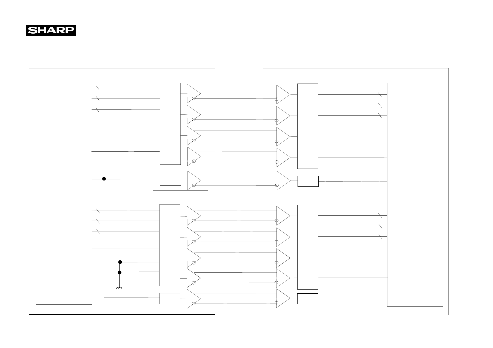
4-2 Interface block diagram
(6)
(12)
)
)
)
(11)
)
)
)
)
)
)
(14)
)
Using receiver:Contained in a control IC.
Corresponding Transmitter:THC63LVDM83R(THine electronics),DS90C383,DS90C383A(National semiconductor)
(Computer side)
LD-14115-5
(TFT-LCD side)
RA0~RA7
GA0~GA7
BA0~BA7
DEA
CLK
Controller
RB0~RB7
GB0~GB7
BB0~BB7
DEB
8
8
8
TTL parallel → LVDS
PLL
RAIN0+(5)
RAIN0-
RAIN1+(8)
RAIN1-(9)
RAIN2+(11)
RAIN2-
RAIN3+(17
RAIN3-(18)
RACLKIN+
RACLKIN-(15
LVDS → TTL parallel
PLL
8
RA0~RA7
8
GA0~GA7
8
BA0~BA7
DEA
CLK
A Port
B Port
8
8
8
TxIN18~20
TTL parallel → LVDS
RBIN0+(5
RBIN0-(6
RBIN1+(8
RBIN1-(9)
RBIN2+
RBIN2-(12
RBIN3+(17
RBIN3-(18
LVDS → TTL parallel
8
RB0~RB7
8
GB0~GB7
8
BB0~BB7
DEB
Internal circuits
RBCLKIN+(14
PLL
RBCLKIN-(15
PLL
Page 9

< SELLVDS= Low >
CKAIN+
CK^AIN-
RAIN0+
RAIN0-
RAIN1+
RAIN1-
RAIN2+
RAIN2-
LD-14115-6
1 cycle
GA0 RA5 RA4 RA3 RA2 RA1 RA0RA0RA1 GA0
BA1 BA0 GA5 GA4 GA3 GA2 GA1GA1GA2 BA1
DEA BA5 BA4 BA3 BA2BA2BA3 DEANA NA
RAIN3+
RAIN3-
CKBIN-
CKBIN+
RBIN0+
RBIN0-
RBIN1+
RBIN1-
RBIN2+
RBIN2-
BA7 BA6 GA7 GA6 RA7 RA6RA6RA7 NANA
Tcsq
GB0 RB5 RB4 RB3 RB2 RB1 RB0RB0RB1 GB0
BB1 BB0 GB5 GB4 GB3 GB2 GB1GB1GB2 BB1
DEB BB5 BB4 BB3 BB2BB2BB3 DEBRSV1 NA
RBIN3+
RBIN3-
DE: Display Enable
RSV1: Reserve (Fixed GND)
NA: Not Available
BB7 BB6 GB7 GB6 RB7 RB6RB6RB7 NANA
Page 10

< SELLVDS= High >
CKAIN+
CKAIN-
RAIN0+
RAIN0-
RAIN1+
RAIN1-
RAIN2+
RAIN2-
LD-14115-7
1 cycle
GA2 RA7 RA6 RA5 RA4 RA3 RA2RA2RA3 GA2
BA3 BA2 GA7 GA6 GA5 GA4 GA3GA3GA4 BA3
DEA BA7 BA6 BA5 BA4BA4BA5 DEANA NA
RAIN3+
RAIN3-
CKBIN-
CKBIN+
RBIN0+
RBIN0-
RBIN1+
RBIN1-
RBIN2+
RBIN2-
BA1 BA0 GA1 GA0 RA1 RA0RA0RA1 NANA
Tcsq
GB2 RB7 RB6 RB5 RB4 RB3 RB2RB2RB3 GB2
BB3 BB2 GB7 GB6 GB5 GB4 GB3GB3GB4 BB3
DEB BB7 BB6 BB5 BB4BB4BB5 DEBRSV1 NA
RBIN3+
RBIN3-
DE: Display Enable
RSV1: Reserve (Fixed GND)
NA: Not Available
BB1 BB0 GB1 GB0 RB1 RB0RB0RB1 NANA
Page 11

4-2. Back light driving
CN 1, 2, 3 (Upside)
CN 4, 5, 6 (Downside)
LD-14115-8
The module-side connector
The user-side connector
Pin no. symbol I/O Function
1
2
V
V
high
low
I Power supply (High voltage side)
I Power supply (Low voltage side)
:
BHSR-02VS-01 (JST)
:
SM02B-BHSS-1-TB (JST)
TFT LCD
1pin
1pin
1pin
CN1
CN2
CN3
1pin
1pin
1pin
5. Absolute Maximum Ratings
Parameter Symbol Condition Ratings Unit Remark
V
Ta=25
Input voltage
+12.0V supply voltage Vcc
Storage temperature Tstg
Operating temperature (Ambient) Topa
Note1】Humidity:95%RH Max. ( Ta≦40℃ )
【
Maximum wet-bulb temperature at 39℃ or less. ( Ta>40℃ )
No condensation.
I
℃-
Ta=25℃ 0 ~ +14.0
-
-
0.3 ~ +3.6
-25 ~ +60
0 ~ +50
CN4
CN5
CN6
V
SELLVDS
V
℃【
℃
Note1
】
Page 12

6. Electrical Characteristics
LD-14115-9
6-1. TFT-LCD panel driving Ta=25
Parameter Symbol Min. Typ. Max. Unit Remark
Note1
Vcc Supply voltage Vcc +11.4 +12.0 +12.6 V
Current dissipation Icc
Permissive input ripple voltage V
Input voltage (Low)
Input voltage (High)
Input current (Low)
Input current (High)
Output voltage (Low)
Output voltage (High)
Note1
【
】
1)On-off sequences of Vcc and data
RF
V
IL
V
IH
I
IL
I
IH
V
OL
V
OH
Vcc Vcc
-
390 600 mA
--
0
+2.7
-
-
--
--
--
2.4
--
11.4V 11.4V
100 mVp-p
+0.6 V SELLVDS
+3.3 V SELLVDS
A
500
100
μ
μ
A
0.4 V BLON:I
V
【
Note2
【
SELLVDS
=GND
V
I
SELLVDS
V
I
BLON:I
=Vcc
OL
OH
0<t1≦60ms
0<t2≦10ms
0≦t3≦1s
1.0V
1.0V
℃
】
】
=-1mA
=1mA
DE,CK,Data DE,CK ,Data
t4≧100ms
2)Dip conditions for supply voltage
Vmin,Vth=11.4V, 9.6V
1) Vth ≦Vcc< Vmin
td≦ 20ms
2) Vcc<Vth
The LCD module shuts down.
Note2】 Typical current situation : 256-gray-bar pattern
【
Vcc=+12.0V
The explanation of each gray scale ,GS,
is described below section 8.
t3 t4 t1 t2
Vcc
Vth Vmin
td
RGB
RGB
GS0
GS1
RGB
GS2
....
RGB
GS254
RGB
GS255
Page 13

6-2. Back light driving
The back light system is an edge-lighting type with six CCFTs (Cold Cathode Fluorescent Tube).
The characteristics of the lamp are shown in the following table.
The value mentioned below is at the case of one CCFT.
CCFT Model Name:KTBE26MSTF‐A424NE209‐Z‐3(STANLEY.ELECTRIC.CO.,LTD)
Parameter Symbol Min. Typ. Max. Unit Remark
Lamp current range I
Lamp voltage V
Lamp power consumption P
Lamp frequency F
L
L
L
L
Kick-off voltage Vs
Lamp life time T
Note1】 A lamp can be light in the range of lamp current shown above.
【
L
3.0 6.0 6.5 mArms
-
-
790
4.7
-
-
30 60 70 KHz
--
--
50,000
--
1,500 Vrms
2,000 Vrms
Maximum rating for current is measured by high frequency current measurement equipment
connected to V
at circuit showed below.
LOW
(Note : To keep enough kick-off voltage and necessary steady voltage for CCFT.)
Lamp frequency : 30~70kHz
Ambient temperature : 0~50
℃
Vrms
W
Hour
Note1
【
Ta=25
Note2
【
Note3
【
Ta=25
Ta=0
Note5
【
】
℃
】
】
℃【
℃【
】
Note4
Note4
LD-14115-10
】
】
CN1:1,2,3,4,5,6:
1pin(Vhigh)
Module
Note2】 Referential data per one CCFT by calculation ( I
【
CN1:1,2,3,4,5,6:
2pin(Vlow)
× V
L
A
~
L ) .
Inverter
The data doesn’t include loss at inverter .
【Note3】 Lamp frequency of inverter may produce interference with horizontal synchronous frequency, and
this may cause horizontal beat on the display. Therefore, adjust lamp frequency, and keep inverter as far
as from module or use electronic shielding between inverter and module to avoid interference.
Note4】Kick-off voltage value is described as the index in the state of lamp only.
【
The kick-off voltage is estimated to be risen up as approx. +200V in the state of module only, and the
further rise up can be seen according to the assembling status of user cabinet. Please set the kick-off
voltage of inverter to avoid the lighting failures in the state of operation. Please design the inverter so
that its open output voltage can be connected for more than 1 second to startup. Otherwise, the lamp
may not be turned on. But, please set as 100ms when the ambient luminance around the lamp is more
than 1lux.
Note5】 Lamp life time is defined as the time when either ① or ② occurs in the continuous operation under
【
《
Note
the condition of Ta=25℃ and I
Brightness becomes 50% of the original value under standard condition.
①
Kick-off voltage at Ta=0℃ exceeds maximum value,2000Vrms .
②
》
=6.0 mArms .
L
The performance o f th e ba ck lig ht , fo r ex ampl e li fe time or bri gh tn es s, is much inf luenced by the characterist ic s
of the DC-AC inverte r for t he lamp. Wh en you desi gn or ord er th e in ver ter, pl ea se make sur e tha t a po or ligh tin g
caused by the mismatch of the backlight and the inverter (miss-lighting, flicker, etc.) never occurs. When you
confirm it, the module should be operated in the same condition as it is installed in your instrument.
Use the lamp inverter power source incorporating such safeguard as overvoltage / overcurrent protective circuit
or lamp voltage waveform detection circuit, which should have individual control of each lamp.
In case one circuit with ou t su c h in d ivid ua l co n tr ol is co n nec ted to more than two lamps, ex ce ssi ve c urr en t may
flow into one lamp when the other one is not in operation.
Synchronize frequency and phase of two CCFT in the same connector.
Otherwise it may exceed rated voltage of connector.
Page 14

7. Timing characteristics of input signals
7-1-1. Timing characteristics
Parameter Symbol Min. Typ. Max. Unit Remark
Clock Frequency 1/Tc 60.0 81.0 85.0 MHz
Skew Tcsq –4 0 4 ns
LD-14115-11
Note1
【
】
Data enable 830 1080 1600 clock
signal
Horizontal period TH
10.0 13.3
-
µs
Horizontal period (High) THd 800 800 800 clock
Note2
1205 1250 2000 line Vertical period TV
12.1 16.7
-
【
ms
Vertical period (High) TVd 1200 1200 1200 line
Note1】 Lvds (A port)– Lvds (B port) phase difference
【
Note2】 In case of using the long vertical period, the deterioration of display quality, flicker etc. may occur.
【
TH
THd
DEA,DEB
DA
(RA,GA,BA)
1599
1 3
1
1599
】
DB
(RB,GB,BB)
DEA,DEB
DEA
DEB
1600
Tc
Tcsq
24
1 2 1200
TV
TVd
2
1600
1199
Page 15

7-2 Input Data Signals and Display Position on the screen
Graphics and texts can be displayed on a 1600 × 3× 1200 dots panel with 16M colors by supplying
48 bit data signal (8bit/color [256 gray scales] × 3 × 2 pixels).
LD-14115-12
RA GA BA RB GB BB
DA(1,1) DB(2,1)
DA(1,1)DB(2,1
DA(1,2) DB(2,2)
DA(1,3)
DA(1,1200)
)
DA(3,1)
Two pixel-data are sampled at the same time.
*DA: RA0~RA7, GA0~GA7, BA0~BA7
*DB: RB0~RB7, GB0~GB7, BB0~BB7
DB(1600,1)
BGR
DB(1600,1200)
Display position of input data(H,V)
Page 16

LD-14115-13
8. Input Signals, Basic Display Colors and Gray Scale of Each Color
Data signal
Colors & Gray RA0 RA1 RA2 RA3 RA4 RA5 RA6 RA7 GA0 GA1 GA2 GA3 GA4 GA5 GA6 GA7 BA0 BA1 BA2 BA3 BA4 BA5 BA6 BA7
Gray scale Scale RB0 RB1 RB2 RB3 RB4 RB5 RB6 RB7 GB0 GB1 GB2 GB3 GB4 GB5 GB6 GB7 BB0 BB1 BB2 BB3 BB4 BB5 BB6 BB7
Black
Blue
Green
Cyan
Red
Basic ColorGray Scale of RedGray Scale of GreenGray Scale of Blue
Magenta
Yellow
White
Black GS0000000000000000000000000
DarkerGS2010000000000000000000000
BrighterGS250101111110000000000000000
GS251011111110000000000000000
RedGS252111111110000000000000000
Black GS0000000000000000000000000
DarkerGS2000000000100000000000000
000000000000000000000000
-
000000000000000011111111
-
000000001111111100000000
-
000000001111111111111111
-
111111110000000000000000
-
111111110000000011111111
-
111111111111111100000000
-
111111111111111111111111
-
GS1100000000000000000000000
GS1000000001000000000000000
BrighterGS250000000001011111100000000
GS251000000000111111100000000
GreenGS252000000001111111100000000
Black GS0000000000000000000000000
GS1000000000000000010000000
DarkerGS2000000000000000001000000
BrighterGS250000000000000000010111111
GS251000000000000000001111111
BlueGS252000000000000000011111111
0 : Low level voltage, 1 : High level voltage.
Each basic color can be displayed in 256 gray scales from 8 bit data signals. According to the combination of
total 48 bit data signals, the 16-million-color display can be achieved on the screen.
Page 17

9. Optical Characteristics
Ta=25℃, Vcc =+12V
Parameter Symbol Condition Min. Typ. Max. Unit Remark
LD-14115-14
Viewing
Angle
range
Vertical
Horizontal
Contrast ratio
Response Rise
Time Decay
Chromaticity of
white
Chromaticity of
red
Chromaticity of
green
Chromaticity of Bx
blue By
Luminance of white
θ
θ
21,θ22
θ
11
12
CR≧10
70 85
70 85
70 85
CR θ=0°-
d
τ
τ
Wx
Wy
Rx
Ry
Gx
Gy
r
-
-
0.283 0.313 0.343
0.299
0.608
0.309
0.250
0.570
0.114
0.057
Y
L
180 220
-
-
-
350
-
525
20 50
0.329
0.638
0.339
0.280
0.600
0.144
0.087
0.359
0.668
0.369
0.310
0.630
0.174
0.117
-
Deg.
Deg
Deg.
ms
ms
-
-
-
-
-
-
-
-
cd/m
2
Note1,4
【
【
【
【
IL=6.0mA rms
【
Note2,4
Note3,4
Note4
Note4
】
】
】
】
】
w
White Uniformity
The measurement shall be executed 30 minutes after
※
δ
--
ghting at rating.
li
1.25
-
【
Note5
】
The optical characteristics shall be measured in a dark room or equivalent state with the method
shown in Fig.2 below.
Photodetector
Contrast ratio/Response Time(BM-5A)
Luminance(BM-7)
Photodetector(EZ-CONTRAST)
400mm
Chromaticity(SR-1)
Field=2°
Center of screen(θ=0°)
TFT-LCD-Module
Center of screen(θ=0°)
TFT-LCD-Module
Fig2-1 Viewing angle measurement method
Fig2 Optical characteristics measurement method
Fig2-2 Luminance/Contrast ratio/Response time/Chromaticity
measurement method
Page 18

Note1】Definitions of viewing angle range:
【
Note2】Definition of contrast ratio:
【
The contrast ratio is defined as the following.
Luminance (brightness) with all pixels white
Contrast Ratio (CR)
=
Luminance (brightness) with all pixels black
Note3】Definition of response time:
【
The response time is defined as the following figure and shall be measured by
LD-14115-15
switching the input signal for "black" and "white".
Note4】This shall be measured at center of the screen.
【
Note5】Definition of white uniformity:
【
White uniformity is defined as the
following with five measurements
(A~E).
pixel1200400 800
δw=
A
C
B
D
E
300
600
900
pixel
Maximum Luminance of five points (brightness)
Minimum Luminance of five points (brightness)
Page 19

LD-14115-16
10. Handling Precautions
a) Be sure to turn off the power supply when inserting or disconnecting the cable.
b) Be sure to design the cabinet so that the module can be installed without any extra stress such as warp or
twist.
c) Since the front polarize is easily damaged, pay attention not to scratch it.
d) Since long contact with water may cause discoloration or spots, wipe off water drop immediately.
e) When the panel surface is soiled, wipe it with absorbent cotton or other soft cloth.
f) Since the panel is made of glass, it may break or crack if dropped or bumped on hard surface. Handle with
care.
g) Since CMOS LSI is used in this module, take care of static electricity and take the human earth into
consideration when handling.
h) Make sure the mounting holes of the module are grounded sufficiently. Take electro-magnetic interference
(EMI) into consideration.
i) The module has some printed circuit boards (PCBs) on the back side. Take care to keep them form any
stress or pressure when handling or installing the module; otherwise some of electronic parts on the PCBs
may be damaged.
j) Observe all other precautionary requirements in handling components.
k) When some pressure is added onto the module from rear side constantly, it causes display non-uniformity
issue , functional defect, etc. So, please avoid such design.
l) If the stress is applied onto the panel under operating conditions, display defects such as black dots may
occur. So, do not press the display with fingers.
To recover this defect, turn off the power supply and restart after several seconds.
11. Packing form
a) Piling number of cartons : maximum 8 cartons
b) Packing quantity in one carton : 2 module
c) Carton size : 592mm(W) × 486mm(H) × 215(D)
d) Total mass of one carton filled with full modules : 10.5kg
e) Packing form is shown in Fig.3
Page 20

12.Reliability test items
No. Test item Conditions
LD-14115-17
1 High temperature storage test
2 Low temperature storage test
3 High temperature
& high humidity operation test
4 High temperature operation test
5 Low temperature operation test
6 Vibration test
(non- operating)
7 Shock test
(non- operating)
Ta=60℃ 240h
Ta=-25℃ 240h
Ta=40℃ ; 95%RH 240h
(No condensation)
Ta=50℃ 240h
(The panel temp. must be less than 60℃)
Ta=0℃ 240H
Frequency : 10~57Hz/Vibration width (one side) : 0.075mm
: 58~500Hz/Gravity : 9.8m/s
2
Sweep time : 11 minutes
Test period : 3 hours
(1 hour for each direction of X,Y,Z)
Max. gravity : 490m/s
2
Pulse width : 11ms, sine wave
Direction : ±X, ±Y, ±Z,
once for each direction.
Result Evaluation Criteria
【
】
Under the display quality test conditions with normal operation state, these shall be no change
which may affect practical display function.
Page 21

13.Others
1) Lot No. and indication Bar Code Label:
LD-14115-18
SHARP
LQ201U1LW01
23 XXXXXX
① Model No. (LQ201U1LW01) ② Lot No. (Date) ③ Quantity
MADE IN JAPAN
2) Packing Label
社内品番:
LotNO. :
Quantity:
ユーザ品番 :
シャープ物流用ラベルです。
(4S)
(4S)LQ201U1L W01
(4S)(4S)
Bar Code
Bar Code
Bar Code
(①)
(1T)2002.03.01
(②)
(Q) 2 pcs
(③)
LQ201U1LW01
LQ201U1LW01LQ201U1LW01
Model No.
Bar Code(Lot No.)
Lot No.
A production year
(the last figures of
the Christian Era)
A production month (1~9,X,Y,Z)
How to express Lot No.
Serial No.
3) Adjusting volume have been set optimally before shipment, so do not change any adjusted value.
If adjusted value is changed, the specification may not be satisfied.
4) Disassembling the module can cause permanent damage and should be strictly avoided.
5) Please be careful since image retention may occur when a fixed pattern is displayed for a long time.
6) The chemical compound that causes the destruction of ozone layer is not being used.
7) Warning of mercury and material information of LPG(Light Pipe Guide) are labeled on the back of the
module.
MATERIAL INFORMATION
MATERIAL INFORMATION
MATERIAL INFORMATIONMATERIAL INFORMATION
>PLASTIC LIGHT GUIDE:PMMA<
>PLASTIC LIGHT GUIDE:PMMA<
>PLASTIC LIGHT GUIDE:PMMA<>PLASTIC LIGHT GUIDE:PMMA<
COLD CATHODE FLUORESCENT LAMP IN LCD PANEL
CONTAINS A SMALL AMOUNT OF MERCURY,PLEASE FOLLOW
LOCAL ORDINANCES OR REGULATION FOR DISPOSAL
当該液晶ディスプレイパネルは蛍光管が組み込まれていますので、地方自
冶体の条例、または、規則に従って廃棄ください。
8) When any question or issue occurs, it shall be solved by mutual discussion.
Page 22

14.Carton storage condition
LD-14115-19
Temperature 0℃ to 40
Humidity 95%RH or less
Reference condition : 20℃ to 35℃ , 85%RH or less (summer)
: 5℃ to 15℃ , 85%RH or less (winter)
the total storage time (40℃,95%RH) : 240H or less
・
Sunlight Be sure to shelter a product from the direct sunlight.
Atmosphere Harmful gas, such as acid and alkali which bites electronic components and/or
wires, must not be detected.
Notes Be sure to put cartons on palette or base, don’t put it on floor, and store them with
removing from wall.
Please take care of ventilation in storehouse and around cartons, and control
changing temperature is within limits of natural environment.
Storage period 1 year
℃
Page 23

LD-14115-20
Page 24

LD-14115-21
Page 25

LD-14115-22
Page 26

SPECIFICATIONS ARE SUBJECT TO CHANGE WITHOUT NOTICE.
Suggested applications (if any) are for standard use; See Important Restrictions for limitations on special applications. See Limited
Warranty for SHARP’s product warranty. The Limited Warranty is in lieu, and exclusive of, all other warranties, express or implied.
ALL EXPRESS AND IMPLIED WARRANTIES, INCLUDING THE WARRANTIES OF MERCHANTABILITY, FITNESS FOR USE AND
FITNESS FOR A PARTICULAR PURPOSE, ARE SPECIFICALLY EXCLUDED. In no event will SHARP be liable, or in any way responsible,
for any incidental or consequential economic or property damage.
NORTH AMERICA
SHARP Microelectronics of the Americas
5700 NW Pacific Rim Blvd.
Camas, WA 98607, U.S.A.
Phone: (1) 360-834-2500
Fax: (1) 360-834-8903
Fast Info: (1) 800-833-9437
www.sharpsma.com
TAIWAN
SHARP Electronic Components
(Taiwan) Corporation
8F-A, No. 16, Sec. 4, Nanking E. Rd.
Taipei, Taiwan, Republic of China
Phone: (886) 2-2577-7341
Fax: (886) 2-2577-7326/2-2577-7328
CHINA
SHARP Microelectronics of China
(Shanghai) Co., Ltd.
28 Xin Jin Qiao Road King Tower 16F
Pudong Shanghai, 201206 P.R. China
Phone: (86) 21-5854-7710/21-5834-6056
Fax: (86) 21-5854-4340/21-5834-6057
Head Office:
No. 360, Bashen Road,
Xin Development Bldg. 22
Waigaoqiao Free Trade Zone Shanghai
200131 P.R. China
Email: smc@china.global.sharp.co.jp
EUROPE
SHARP Microelectronics Europe
Division of Sharp Electronics (Europe) GmbH
Sonninstrasse 3
20097 Hamburg, Germany
Phone: (49) 40-2376-2286
Fax: (49) 40-2376-2232
www.sharpsme.com
SINGAPORE
SHARP Electronics (Singapore) PTE., Ltd.
438A, Alexandra Road, #05-01/02
Alexandra Technopark,
Singapore 119967
Phone: (65) 271-3566
Fax: (65) 271-3855
HONG KONG
SHARP-ROXY (Hong Kong) Ltd.
3rd Business Division,
17/F, Admiralty Centre, Tower 1
18 Harcourt Road, Hong Kong
Phone: (852) 28229311
Fax: (852) 28660779
www.sharp.com.hk
Shenzhen Representative Office:
Room 13B1, Tower C,
Electronics Science & Technology Building
Shen Nan Zhong Road
Shenzhen, P.R. China
Phone: (86) 755-3273731
Fax: (86) 755-3273735
JAPAN
SHARP Corporation
Electronic Components & Devices
22-22 Nagaike-cho, Abeno-Ku
Osaka 545-8522, Japan
Phone: (81) 6-6621-1221
Fax: (81) 6117-725300/6117-725301
www.sharp-world.com
KOREA
SHARP Electronic Components
(Korea) Corporation
RM 501 Geosung B/D, 541
Dohwa-dong, Mapo-ku
Seoul 121-701, Korea
Phone: (82) 2-711-5813 ~ 8
Fax: (82) 2-711-5819
 Loading...