

Page 1
www.jxlcd.com
www.jxlcd.com
Page 2

www.jxlcd.com
www.jxlcd.com
Page 3
N
N
REVISION HISTORY
Revision Date Prepared Checked Approved Summary
A
1st issue.
T.Ito
F.Yamada
F.Yamada
Change manufacture
to SHARP.
RoHS standard
conformed pro duc t.
Change manufacture
to SHARP.
④
01A
02A
Aug. 11,2004
Feb. 8,2005 E.Nitto
K. Nukiyama K.Tanaka
K.Yonemura
B
C C
www.jxlcd.com
D
www.jxlcd.com
D
E
TITLE
20050420 S.Fukutoku T.Ito Revised P3,19,23,26,31,33-36
05
DATE DOCUMENT CONTROL SECTION
20050208 E.Nitto K.Yonem ura T.Ito Add revision 02A,reviced P31
04
03
20041125 E.Nitto T.Ito Reviced P8,19,37
20040826 K.Nukiyama T. Ito Revised P2,22,27
02
EDIT
DATE
DESIG.
DESIG. DESCRIPTION
20040811 K.Nukiyama K.Yonemura K.Tanaka
CHECK
1
APPR.
CHECK
APPR.
DRAW. NO.
ARP CORPOR ATION
SH
SHARP CORPORATIO
ARP CORPOR ATIONARP CORPOR ATIO
SHSH
LQ190E1LX31
( FLC48SXC8V-12)
LD17426
SHEET
1
/
CUST.
38
Page 4
N
N
TABLE OF CONTENTS
A
B
C C
D
1.APPLICATIONS
2.PRODUCT NAME AND MODEL NUMBER
2-1.Product Name
2-2.Model Number
3.OVERVIEW
4.CONFIGURATION
5.MECHANICAL SPECIFICATIONS
6.ABSOLUTE MAXIMUM RATING
7.RECOMMENDED OPERATING CONDITIONS
8.ELECTRICAL SPECIFICATIONS
9.OPTICAL SPECIFICATIONS
10.INTERFACE SPECIFICATIONS
10-1.Signal Descriptions
10-2.LVDS Data Assignment
10-3. Color Data Assignment
10-4. Input Signal Timing
10-5. Correspondence between Data and Display Position
10-6.Power Supply Sequence
11.BACK-LIGHT SPECIFI CATIONS
11-1.Pin configuration for Back-light
11-2.Life
www.jxlcd.com
11-3.Lamp assembly set
www.jxlcd.com
12.APPEARANCE SPECIFICATIONS
12-1.Appearance
12-2.Dot defects
13.ENVIRONMENTAL SPECIFICATIONS
14.INDICATIONS
15.P ACKAGING
15-1.Packing Specifications
15-2.Packing Method
16.WARRANTY
17.PRECAUTIONS
18.PRECAUTIONS FOR USE
19.MISCELLANEOUS
3
3
3
3
3
3
4
5
5
6
8
12
12
13
15
16
18
18
19
19
19
19
20
20
21
22
23
23
23
23
29
29
36
36
D
E
TITLE
DATE DOCUMENT CONTROL SECTION
EDIT
DESIG.
DATE
DESIG. DESCRIPTION
CHECK
APPR.
CHECK
APPR.
DRAW. NO.
SHARP CORPO R ATION
SHARP CORPO R ATIO
SHARP CORPO R ATIONSHARP CORPO R ATIO
LQ190E1LX31
( FLC48SXC8V-12)
LD17426
SHEET
2
/
CUST.
1
Page 5

N
N
1. APPLICA TION
1. APPLICA TION
1. APPLICA TION1. APPLICA TION
This specification is applied to the 19-inch SXGA supported TFT-LCD module.
A
2222.... PRODUCT NAME AND MODEL NUMBER
PRODUCT NAME AND MODEL NUMBER
PRODUCT NAME AND MODEL NUMBER PRODUCT NAME AND MODEL NUMBER
2–1 Product Name : LCD Modul
2–2 Model Name
B
3. OVERVIEW
3. OVERVIEW
3. OVERVIEW3. OVERVIEW
This LCD module has a TFT active matrix type liquid crystal panel 1280x1024 pixels, and
diagonal size of 48cm(19-inch). This LCD has a LVDS dual interface and can display
16,777,216 colors.
2
○
This module includes Fast Response time Driving circuit.
C C
The power supply of this LCD module is +5V DC voltage.
: LQ190E1LX31
LCD Moduleeee
LCD ModulLCD Modul
(FLC48SXC8V-12)
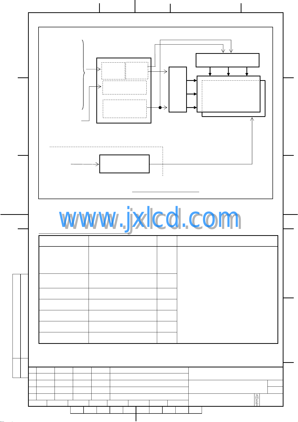
4. CONFIGURATION
4. CONFIGURATION
4. CONFIGURATION4. CONFIGURATION
D
www.jxlcd.com
www.jxlcd.com
This LCD module consists of a color TFT-LCD panel that is mounted with TFT driver ICs
and a cold-cathode fluorescent tube back-light.
The inverter for the back-light is not included.
Figure 4-1 shows a block diagram of this LCD module.
D
E
DATE DOCUMENT CONTROL SECTION
20050420 The model name was changed.
05
02 20040826 Correction of overview.
EDIT
DATE
DESIG.
DESIG. DESCRIPTION
CHECK
1
APPR.
CHECK
APPR.
TITLE
DRAW. NO.
SHARP CORPO R ATION
SHARP CORPO R ATIO
SHARP CORPO R ATIONSHARP CORPO R ATIO
LQ190E1LX31
( FLC48SXC8V-12)
LD17426
SHEET
3
/
CUST.
Page 6
N
N
Input signals (L VDS Dual)
RXO0+
A
B
C C
RXO0-
RXO1+
RXO1RXO2+
RXO2-
RXO3+
RXO3-
RXOC+
RXOC-
PD
SEL LVDS
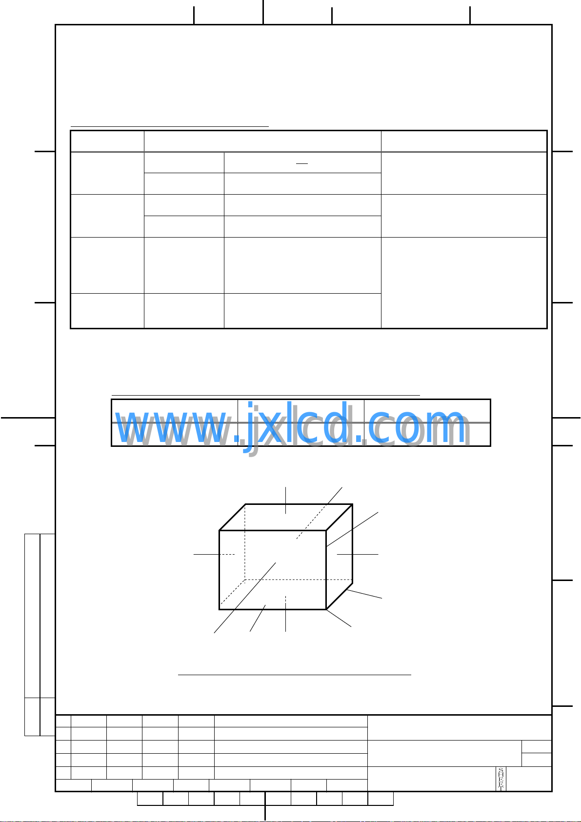
5. MECHANICAL SPECIFICATIONS
5. MECHANICAL SPECIFICATIONS
5. MECHANICAL SPECIFICATIONS5. MECHANICAL SPECIFICATIONS
Ta ble 5-1 shows the mechanical specifications of this LCD module.
Table 5-1 Mechanical Specifications
RXE0+
RXE0-
RXE1+
RXE1RXE2+
RXE2-
RXE3+
RXE3-
RXEC+
RXEC-
Vcc
(+5V)
Power
supply
www.jxlcd.com
www.jxlcd.com
LVDS
Receiver
DC/DC converter
Bias voltage
Supply circuit
(Separate)
Inverter circuit
Internal
Circuit
Figure 4-1 Block Diagram
RSDS I/F
Gate
Driver
Data driver
TFT color LCD panel
1280x3(RGB)x1024
Back-light
(6 CCFL)
Item Specifications Unit Remark
D
Dimensions
Display
Resolution
Display Dot Area
Dot Pitch
Pixel Aspect Ratio
Weight 3,200 MAX.
FG-SG Short circuit —
DATE DOCUMENT CONTROL SECTION
EDIT
DATE
DESIG.
DESIG. DESCRIPTION
CHECK
1
404.2x330x22(TYP.)
(1280x3)x1024
376.32x301.056
(0.098x3)x0.294
1:1 —
APPR.
CHECK
APPR.
mm
—
mm
mm
g
Edge type back-light is used.
(CCFLx6)
Without inverter.
For details on dimensions,
see dimensional outline drawing.
(Figure 20-1,2)
Excluding inverter.
TITLE
DRAW. NO.
SHARP CORPO R ATION
SHARP CORPO R ATIO
SHARP CORPO R ATIONSHARP CORPO R ATIO
LQ190E1LX31
( FLC48SXC8V-12)
LD17426
D
E
CUST.
SHEET
4
/
Page 7

N
N
6. ABSOLUTE MAXIMUM RATING
6. ABSOLUTE MAXIMUM RATING
6. ABSOLUTE MAXIMUM RATING6. ABSOLUTE MAXIMUM RATING
Table 6- 1 sh ows the absolute maximum rating of this LCD module.
A
B
Table 6-1 Absolute Maximum Rating
Item Symbol Condition MIN. TYP. MAX. Unit
Supply Voltage VCC Ta=25ºC –0.3 — 6.0 V
Input Signal Voltage
(LVDS signal,
PD,SEL LVDS )
7. RECOMMENDED OPERATING CONDITIONS
7. RECOMMENDED OPERATING CONDITIONS
7. RECOMMENDED OPERATING CONDITIONS7. RECOMMENDED OPERATING CONDITIONS
Ta ble 7-1 shows the recommended operating conditions of this LCD module.
Ta ble 7-1 Recommen de d Operating Conditions
Ta=25ºC –0.3 — 3.6 V
V
IN
Item Symbol MIN. TYP. MAX. Unit
C C
D
Supply Voltage(Logi c) V
Ripple Voltage V
www.jxlcd.com
www.jxlcd.com
CC
CC
V
RP
4.75 — 5.25 V
— — 0.1 V
D
E
DATE DOCUMENT CONTROL SECTION
EDIT
DATE
DESIG.
DESIG. DESCRIPTION
CHECK
1
APPR.
CHECK
APPR.
TITLE
DRAW. NO.
SHARP CORPO R ATION
SHARP CORPO R ATIO
SHARP CORPO R ATIONSHARP CORPO R ATIO
LQ190E1LX31
( FLC48SXC8V-12)
LD17426
SHEET
5
/
CUST.
Page 8
N
N
8. ELECTRICAL SPECIFICATIONS
8. ELECTRICAL SPECIFICATIONS
8. ELECTRICAL SPECIFICATIONS8. ELECTRICAL SPECIFICATIONS
Table 8-1 shows the electrical specifications of this LCD module. Figure 8-1 shows the
A
measurement circuit. Figure 8-2(A) shows the equivalent circuit of the logic signal input area.
Figure 8-2(B) shows the equivalent circuit of the supply voltage Input area.
Table 8-1 Electrical Specifications
Item Symbol Condition MIN. TYP. MAX. Unit
Differential-input
Voltage (Hign)
V
IH
— — 100 mV
Remark
VCM=+1.2V
Differential-input
Voltage (Low)
B
Input V oltage (High) V
V
IL
IH
Input Voltage (Low) VIL 0 — 0.8 V
–100 — — mV
2.0 — 3.3 V
PD
SEL
LVDS
VCC=+5.0±0.25V
=0V
V
Supply Current I
CC
SS
DCLK=54MHz
— 900 1500 mA *1
Ta=25º C
Supply Rush Curre nt I
SCC
— — 3.5 A
*2
Supply Rush Curre nt
C C
Duration(1.5A excess)
T
SCC
— — 1.0 ms
BACK
CCFL T urn on
Voltage
V
fL=50kHz,Ta=25ºC — 1400 1600
S
fL=50kHz,Ta=0ºC — 1500 1600
Vrms
LIGHT
D
www.jxlcd.com
Lighting Voltage V
Lighting Freque ncy f
www.jxlcd.com
(*3)
T u be C urrent I
fL=50kHz
L
L
L
=7mA
I
L
VL=750Vrms 40 50 60 kHz
fL=50kHz
=750Vrms
V
L
— 750 — Vrms
4 7 8
mArms
*3
D
(*1) Typical current situation : Color bar pattern. Vcc=5.0V
Maximum current situation : Whit e pattern. Vcc=4.75V
Without rush curre nt.
(*2) These items prescribe the rush current for starting internal DC/DC.
Charging current to capacitors of Vcc is not prescribed.
(*3) T u be current (I
) shows the value of the current that is consumed at one lamp.
L
This LCD module has 6 lamp s. Each 3 lamps are placed at upper side and
lower side of the display.
E
3 lamps is connected in parallel. Each low voltage terminals are connected with separate
cable to Back-light conn ecter.
DATE DOCUMENT CONTROL SECTION
TITLE
DRAW. NO.
EDIT
DESIG.
DATE
DESIG. DESCRIPTION
CHECK
APPR.
CHECK
APPR.
ARP CORPOR ATION
SH
SHARP CORPORATIO
ARP CORPOR ATIONARP CORPOR ATIO
SHSH
LQ190E1LX31
( FLC48SXC8V-12)
LD17426
SHEET
6
/
CUST.
1
Page 9

N
N
V
Measurement circuit is based on Figure 8-1.
+5V
A
GND
AC
B
GND
Input signals (L VDS Dual)
RXO0+
RXO0-
RXO1+
RXO1RXO2+
RXO2-
RXO3+
C C
RXO3-
RXOC+
RXOC-
D
RXE0+
RXE0-
RXE1+
RXE1RXE2+
RXE2-
RXE3+
RXE3-
RXEC+
RXEC-
SEL LVDS
www.jxlcd.com
www.jxlcd.com
Vs
PD
CL
Icc
Vcc
DC/DC
Converter
I
L
Figure 8-1 Measurement circuit
Differential
Input
+
−
+3.3V
10kΩ(Pull-up)
50kΩ
(Pull-down)
0V
Figure 8-2(A) Equivalent circuit of logic signal Input
100Ω
Logic Analog Driver
Back-light
T-CON
LCD module
Internal
circuit
D
FB
CHECK
Fuse
FG(Frame ground)
Figure 8-2(B) Equivalent circuit of power supply
APPR.
CHECK
cc
GND
DATE
DESIG. DESCRIPTION
1
DATE DOCUMENT CONTROL SECTION
EDIT
DESIG.
FB
APPR.
100pF
TITLE
DRAW. NO.
SHARP CORPO R ATION
SHARP CORPO R ATIO
SHARP CORPO R ATIONSHARP CORPO R ATIO
10μF
LQ190E1LX31
( FLC48SXC8V-12)
LD17426
Internal
Circuit
SHEET
7
/
E
CUST.
Page 10
R
R
N
N
9. OPTICAL SPECIFICATIONS
9. OPTICAL SPECIFICATIONS
9. OPTICAL SPECIFICATIONS9. OPTICAL SPECIFICATIONS
Table 9-1 shows the optical specifications of this LCD module.
A
Table 9-1 Optical Specifications
Ta=25˚C,Signal timing=Typ.
Item Symbol Condition
MIN. TYP. MAX.
Horizontal
Visual
Angle
Contrast Ratio CR
B
Ver ti ca l
All Direction
Response
Time(Rise+Fall)
(B→W→B)
Response
Time (Rise or Fall)
(All gray scale)
Brightness
Brightness Uniformity
C C
W
Chromaticity
www.jxlcd.com
www.jxlcd.com
R
G
B
θ
L,R
θ
θ
U,D
θ
τ
rise
+
τ
fall
τ
avg
I
△I
x
y
(x,y)
θ
=0°
U,D
CR≧10
L,R
=0°
— 80 — deg
θ
L,R,U,D
θ
L,R,
=0°
θ
U,D
L,R,
U,D
=0°
Ta= 25˚C
Ta= 0
Ta= 25
=0°
=5V
CC
=7mA
=0°
θ
L,R,U,D
V
I
L
fL=50kHz
R*,G*,B* Signal
=All “H”
Red
Green
Blue
˚C
ºC
85 89 — deg
85 89 — deg
400
○
950
— —
3
600
— 12 — ms
— 24 — ms
— 8 — ms
3
320
○
360
450 — cd/m
70 — —
0.283 0.313 0.343
0.299 0.329 0.359
40 , 0.349 ) Typ.
( 0.6
3
○
( 0.645 , 0.347 ) Typ.
83 , 0.598 ) Typ.
( 0.2
3
○
( 0.279 , 0.597 ) Typ.
( 0.1
42 , 0.071 ) Typ.
3
○
( 0.142 , 0.068 ) Typ.
Unit
%
—
—
2
Note
White/
Black
Average
of
Response
*2
Time,
White
*1
(1)(2)
(3)(5)
(6)
(1)(2)
(3)(5)
(1)
(4)
(5)
(1)(5)
(1)(5)
(7)
(1)
(5)
Specifications Remark
LCD Panel Type TFT Color
D
Display Mode Normaly Black
D
Wide Viewing Angle Technology MVA-Premium
Optimum Viewing Angle — (symmentry) (6)
Display Color 16,777,216 (8-bit color)
Color of non-display area Black
Surface Treatment Glare (Hardness: 2H)
(*1) Value at 15~20 minutes after lighting on.
(*2) In case of applying FLCB-12, (Fast Response Time Driving Circuit)
E
(Note) ・CS-1000 (MINOLTA Co., Ltd.) Field=1°, L=500mm
・Back-light current = 7mA, Dark room condition(1 lux or less)
Be carefull that the luminance meter, which you use, may not be able to get correct brightenss
if it’s no set correctly.
DATE DOCUMENT CONTROL SECTION
03 20041125 Change optical spec.
EDIT
DESIG.
DATE
DESIG. DESCRIPTION
CHECK
APPR.
CHECK
APPR.
TITLE
DRAW. NO.
SHARP CORPO
SHARP CORPORATIO
SHARP CORPORSHARP CORPO
LQ190E1LX31
(FLC48SXC8V-12)
LD17426
ATION
ATIONATIO
CUST.
SHEET
8
/
1
Page 11

R
R
N
N
Note 1) Definition of Viewing Angle (1)
Based on Figure 9-1.
θ
U
*0°(Front)
θ
θ
D
R
X+
Right (3 o’clock Direction)
A
Y+
Top (12 o’clock Direction)
θ
L
LCD module
B
X-
Left (9 o’clock Direction)
*→ θ
=0°,θD=0°,θL=0°,θR=0°
U
Y-
Bottom (6 o’clock Direction)
Figure 9-1 Definition of Viewing Angle (1)
Note 2) Definition of Viewing Angle (2)
C C
Based on Figure 9-2.
www.jxlcd.com
www.jxlcd.com
Display Surface
Display Surface
θ
θ
L,R,U,D
θ
MIN
TYP
θ
MAX
=0°
D
Figure 9-2 Definition of Viewing Angle (2)
Note 3) Definition of Contrast Ratio (CR)
L
W
White
Determined by Formula (1) based on
Figure 9-3 Voltage-Brightness
characteristics.
LW (Brightness at white)
= ……(1)
L
(Brightness at black)
B
Brightness
[L]
L
B
0
0
Black
Panel Drive Voltage [V]
Figure 9-3 Voltage-Brightness Characteristics
D
E
DATE DOCUMENT CONTROL SECTION
TITLE
DRAW. NO.
EDIT
DESIG.
DATE
DESIG. DESCRIPTION
CHECK
APPR.
CHECK
APPR.
SHARP CORPO
SHARP CORPORATIO
SHARP CORPORSHARP CORPO
1
LQ190E1LX31
(FLC48SXC8V-12)
LD17426
ATION
ATIONATIO
CUST.
SHEET
9
/
Page 12
R
R
N
N
p
A
B
Note 4) Definition of Response Time
Based on Figure 9-4.
100%
Relative
Brightnes
0%
τ
0%
rise
1 frame
90%
90%
10%
τ
fall
Note 5) Contrast Ratio and Response Measurement System
C C
D
Based on Figure 9-5.
-
Z
www.jxlcd.com
www.jxlcd.com
-
X
Drive and Measurement System
Figure 9-5 Contrast Ratio and Response Time Measurement System
ON Response Time
Figure 9-4 Definition of Response Time
+
Y
-
Y
OFF Res
onse Time
+
X
+
Z
Brightness Meter or
θ
Luminance colorimeter
(with luminosity
correction function)
D
E
DATE DOCUMENT CONTROL SECTION
.
EDIT
DATE
DESIG.
DESIG. DESCRIPTION
CHECK
1
APPR.
CHECK
APPR.
TITLE
DRAW. NO.
SHARP CORPO
SHARP CORPORATIO
SHARP CORPORSHARP CORPO
LQ190E1LX31
(FLC48SXC8V-12)
LD17426
ATION
ATIONATIO
CUST.
SHEET
10
/
Page 13

A
R
R
N
N
B
Note 6) Definition of Optimum Viewing Angle
MAX
Contrast
Ratio
10
(-)
6 o’clock←
Viewing Angleθ
0
(+)
→12 o’clock
Figure 9-6 Definition of Viewing Angle
Note 7) Definition of Brightness Uniformity
Brightness uniformity is defined by the following formula.
C C
D
Brightness (I1~I9) art measured at the following 9 points (○
that is shown in Figure 9-7.
Brightness Uniformity (△L) = × 100 (%) , n = 1 to 9
www.jxlcd.com
www.jxlcd.com
192 640 1088 Dot
①
②
③
Note) Each measurement point (○
The tolerance of measurement position is±3mm.
④
⑤
⑥
Figure 9-7 Measurement Points
1-○9
) on the display area
|Min. In|
|Max. In|
⑦
⑧
⑨
1-○9
) defines the center spot of view of Brightness Meter.
154
512
870
D
E
DATE DOCUMENT CONTROL SECTION
EDIT
DATE
DESIG.
DESIG. DESCRIPTION
CHECK
1
APPR.
CHECK
APPR.
TITLE
DRAW. NO.
SHARP CORPO
SHARP CORPORATIO
SHARP CORPORSHARP CORPO
LQ190E1LX31
(FLC48SXC8V-12)
LD17426
ATION
ATIONATIO
CUST.
SHEET
11
/
Page 14

R
R
N
N
10. INTERFACE
10. INTERFACE SPECIFICATIONS
10. INTERFACE10. INTERFACE
10-1 Signal descriptions
A
B
C C
D
FI-X30H (Wire type) , FI-X30HL (Wire with lock)
FI-X30C (Coaxial cable type) , FI-X30C2L (Coaxial cable with lock)
*2: When using a connector other than the recommended one , a defect in the initial stage or a
DATE DOCUMENT CONTROL SECTION
EDIT
DESIG.
Table 10-1 shows the description and configuration of interface signals (CN1).
www.jxlcd.com
www.jxlcd.com
Connector : FI-X30SSL-HF (Japan Aviation Electronics)
User’s connector : FI-X30M (FPC type)
*1: Keep open. (Internal test use only.)
problem concerning long term reliability may occur.
DATE
DESIG. DESCRIPTION
1
SPECIFICATIONS
SPECIFICATIONS SPECIFICATIONS
Table 10-1 Interface signals (CN1)
Pin No. Symbol I/O Function
I
I
I
I
I
I
―
I
I
I
I
I
I
―
I
I
―
I
I
I
I
I
―
―
―
―
―
―
APPR.
Negative differential input
Positive differential input
Negative differential input
Positive differential input
Negative differential input
Positive differential input
Ground
Negative differential input
Positive differential input
Negative differential input
Positive differential input
Negative differential input
Positive differential input
Ground
Negative differential input
Positive differential input
Ground
Negative differential input
Positive differential input
Negative differential input
Positive differential input
Negative differential input
Positive differential input
Ground
LVDS Core Power Down
Test pin *1
+5V power supply
+5V power supply
+5V power supply
TITLE
DRAW. NO.
SHARP CORPO
SHARP CORPORATIO
SHARP CORPORSHARP CORPO
CHECK
1
2 RxO0+
3
4 RxO1+
5
6 RxO2+
7 GND
8
9 RxOC+
10
11 RxO3+
12
13 RxE0+
14 GND
15
16 RxE1+
17 GND
18
19 RxE2+
20
21 RxEC+
22
23
24 GND
25 SEL LVDS I Select LVDS Mapping
26 PD
27 TST
28 Vcc
29 Vcc
30 Vcc
APPR.
CHECK
RxO0-
RxO1-
RxO2-
RxOC-
RxO3-
RxE0-
RxE1-
RxE2-
RxEC-
RxE3RxE3+ I
LD17426
LQ190E1LX31
(FLC48SXC8V-12)
SHEET
ATION
ATIONATIO
12
D
E
CUST.
/
Page 15

R
R
N
N
10-2 LVDS Data Assignment
Table 10-2A,10-2B show the LVDS Data Assignment.
Table 10-2A LVDS Data Assignment(SEL LVDS=L)
(SEL LVDS=L)
(SEL LVDS=L)(SEL LVDS=L)
A
Transmitter
Input signal *1
RO2
RO3
RO4
RO5
RO6
RO7
GO2
B
LVD S
Odd
C C
www.jxlcd.com
www.jxlcd.com
D
LVD S
Even
GO3
GO4
GO5
GO6
GO7
BO2
BO3
BO4
BO5
BO6
BO7
RSVD
RSVD
ENAB
RO0
RO1
GO0
GO1
BO0
BO1
RSVD
DCLK 31 TxCLK IN
RE2
RE3
RE4
RE5
RE6
RE7
GE2
GE3
GE4
GE5
GE6
GE7
BE2
BE3
BE4
BE5
BE6
BE7
RSVD
RSVD
RSVD
RE0
RE1
GE0
GE1
BE0
BE1
RSVD
DCLK 31 TxCLK IN
DS90CF383,C385
pin INPUT System side
51
TxIN0
52
54
55
56
3
4
6
7
11
12
14
15
19
20
22
23
24
27
28
30
50
2
8
10
16
18
25
51
52
54
55
56
3
4
6
7
11
12
14
15
19
20
22
23
24
27
28
30
50
2
8
10
16
18
25
TxIN1
TxIN2
TxIN3
TxIN4
TxIN6
TxIN7
TxIN8
TxIN9
TxIN12
TxIN13
TxIN14
TxIN15
TxIN18
TxIN19
TxIN20
TxIN21
TxIN22
TxIN24
TxIN25
TxIN26
TxIN27
TxIN5
TxIN10
TxIN11
TxIN16
TxIN17
TxIN23
TxIN0
TxIN1
TxIN2
TxIN3
TxIN4
TxIN6
TxIN7
TxIN8
TxIN9
TxIN12
TxIN13
TxIN14
TxIN15
TxIN18
TxIN19
TxIN20
TxIN21
TxIN22
TxIN24
TxIN25
TxIN26
TxIN27
TxIN5
TxIN10
TxIN11
TxIN16
TxIN17
TxIN23
Tx OUT0+
Tx OUT0-
Tx OUT1+
Tx OUT1-
Tx OUT2+
Tx OUT2-
Tx OUT3+
Tx OUT3-
TxCLK OUT+
TxCLK OUT-
Tx OUT0+
Tx OUT0-
Tx OUT1+
Tx OUT1-
Tx OUT2+
Tx OUT2-
Tx OUT3+
Tx OUT3-
TxCLK OUT+
TxCLK OUT-
Interface connector
LCD module
pin
2
1
4
3
6
5
11
10
9
8
13
12
16
15
19
18
23
22
21
20
RxO0+
RxO0-
RxO1+
RxO1-
RxO2+
RxO2-
RxO3+
RxO3-
RxCLK IN+
RxCLK IN-
RxE0+
RxE0-
RxE1+
RxE1-
RxE2+
RxE2-
RxE3+
RxE3-
RxCLK IN+
RxCLK IN-
Receiver
DS90CF386
THC63LVDF84
pin OUTPUT
27
RxOUT0
29
RxOUT1
30
RxOUT2
32
RxOUT3
33
RxOUT4
35
RxOUT6
37
RxOUT7
38
RxOUT8
39
RxOUT9
43
RxOUT12
45
RxOUT13
46
RxOUT14
47
RxOUT15
51
RxOUT18
53
RxOUT19
54
RxOUT20
55
RxOUT21
1
RxOUT22
3
RxOUT24
5
RxOUT25
6
RxOUT26
7
RxOUT27
34
RxOUT5
41
RxOUT10
42
RxOUT11
49
RxOUT16
50
RxOUT17
2
RxOUT23
26 RxCLK OUT DCLK
27
RxOUT0
29
RxOUT1
30
RxOUT2
32
RxOUT3
33
RxOUT4
35
RxOUT6
37
RxOUT7
38
RxOUT8
39
RxOUT9
43
RxOUT12
45
RxOUT13
46
RxOUT14
47
RxOUT15
51
RxOUT18
53
RxOUT19
54
RxOUT20
55
RxOUT21
1
RxOUT22
3
RxOUT24
5
RxOUT25
6
RxOUT26
7
RxOUT27
34
RxOUT5
41
RxOUT10
42
RxOUT11
49
RxOUT16
50
RxOUT17
2
RxOUT23
26 RxCLK OUT Not use
LCD
Control
input
RO2
RO3
RO4
RO5
RO6
RO7
GO2
GO3
GO4
GO5
GO6
GO7
BO2
BO3
BO4
BO5
BO6
BO7
Not use
Not use
ENAB
RO0
RO1
GO0
GO1
BO0
BO1
Not use
RE2
RE3
RE4
RE5
RE6
RE7
GE2
GE3
GE4
GE5
GE6
GE7
BE2
BE3
BE4
BE5
BE6
BE7
Not use
Not use
Not use
RE0
RE1
GE0
GE1
BE0
BE1
Not use
D
E
*1 ・RSVD (reserved) pin on a transmitter should be connected with Ground.
・Input odd or even data depending on the display position of the LCD module.
DATE DOCUMENT CONTROL SECTION
EDIT
DESIG.
DATE
DESIG. DESCRIPTION
CHECK
APPR.
CHECK
APPR.
TITLE
DRAW. NO.
SHARP CORPO
SHARP CORPORATIO
SHARP CORPORSHARP CORPO
LQ190E1LX31
(FLC48SXC8V-12)
LD17426
ATION
ATIONATIO
CUST.
SHEET
13
/
1
Page 16
R
R
N
N
Table 10-2B LVDS Data Assignment(SEL LVDS=H)
A
B
C C
D
Input signal *1
RO0
RO1
RO2
RO3
RO4
RO5
GO0
GO1
GO2
GO3
GO4
GO5
BO0
LVD S
Odd
www.jxlcd.com
www.jxlcd.com
LVD S
Even
BO1
BO2
BO3
BO4
BO5
RSVD
RSVD
ENAB
RO6
RO7
GO6
GO7
BO6
BO7
RSVD
DCLK 31 TxCLK IN
RE0
RE1
RE2
RE3
RE4
RE5
GE0
GE1
GE2
GE3
GE4
GE5
BE0
BE1
BE2
BE3
BE4
BE5
RSVD
RSVD
RSVD
RE6
RE7
GE6
GE7
BE6
BE7
RSVD
DCLK 31 TxCLK IN
Transmitter
DS90CF383,C385
pin INPUT System side
51
52
54
55
56
3
4
6
7
11
12
14
15
19
20
22
23
24
27
28
30
50
2
8
10
16
18
25
51
52
54
55
56
3
4
6
7
11
12
14
15
19
20
22
23
24
27
28
30
50
2
8
10
16
18
25
*1 ・RSVD (reserved) pin on a transmitter should be connected with Ground.
・Input odd or even data depending on the display position of the LCD module.
(SEL LVDS=H)
(SEL LVDS=H)(SEL LVDS=H)
TxIN0
TxIN1
TxIN2
TxIN3
TxIN4
TxIN6
TxIN7
TxIN8
TxIN9
TxIN12
TxIN13
TxIN14
TxIN15
TxIN18
TxIN19
TxIN20
TxIN21
TxIN22
TxIN24
TxIN25
TxIN26
TxIN27
TxIN5
TxIN10
TxIN11
TxIN16
TxIN17
TxIN23
TxIN0
TxIN1
TxIN2
TxIN3
TxIN4
TxIN6
TxIN7
TxIN8
TxIN9
TxIN12
TxIN13
TxIN14
TxIN15
TxIN18
TxIN19
TxIN20
TxIN21
TxIN22
TxIN24
TxIN25
TxIN26
TxIN27
TxIN5
TxIN10
TxIN11
TxIN16
TxIN17
TxIN23
Interface connector
Tx OUT0+
Tx OUT0-
Tx OUT1+
Tx OUT1-
Tx OUT2+
Tx OUT2-
Tx OUT3+
Tx OUT3-
TxCLK OUT+
TxCLK OUT-
Tx OUT0+
Tx OUT0-
Tx OUT1+
Tx OUT1-
Tx OUT2+
Tx OUT2-
Tx OUT3+
Tx OUT3-
TxCLK OUT+
TxCLK OUT-
LCD module
pin
RxO0+
2
RxO0-
1
RxO1+
4
RxO1-
3
RxO2+
6
RxO2-
5
9
8
RxO3+
RxO3-
RxCLK IN+
RxCLK IN-
RxE0+
RxE0-
RxE1+
RxE1-
RxE2+
RxE2-
RxE3+
RxE3-
RxCLK IN+
RxCLK IN-
11
10
13
12
16
15
19
18
23
22
21
20
Receiver
DS90CF386
THC63LVDF84
pin OUTPUT
27
RxOUT0
29
RxOUT1
30
RxOUT2
32
RxOUT3
33
RxOUT4
35
RxOUT6
37
RxOUT7
38
RxOUT8
39
RxOUT9
43
RxOUT12
45
RxOUT13
46
RxOUT14
47
RxOUT15
51
RxOUT18
53
RxOUT19
54
RxOUT20
55
RxOUT21
1
RxOUT22
3
RxOUT24
5
RxOUT25
6
RxOUT26
7
RxOUT27
34
RxOUT5
41
RxOUT10
42
RxOUT11
49
RxOUT16
50
RxOUT17
2
RxOUT23
26 RxCLK OUT DCLK
27
RxOUT0
29
RxOUT1
30
RxOUT2
32
RxOUT3
33
RxOUT4
35
RxOUT6
37
RxOUT7
38
RxOUT8
39
RxOUT9
43
RxOUT12
45
RxOUT13
46
RxOUT14
47
RxOUT15
51
RxOUT18
53
RxOUT19
54
RxOUT20
55
RxOUT21
1
RxOUT22
3
RxOUT24
5
RxOUT25
6
RxOUT26
7
RxOUT27
34
RxOUT5
41
RxOUT10
42
RxOUT11
49
RxOUT16
50
RxOUT17
2
RxOUT23
26 RxCLK OUT Not use
LCD
Control
input
RO0
RO1
RO2
RO3
RO4
RO5
GO0
GO1
GO2
GO3
GO4
GO5
BO0
BO1
BO2
BO3
BO4
BO5
Not use
Not use
ENAB
RO6
RO7
GO6
GO7
BO6
BO7
Not use
RE0
RE1
RE2
RE3
RE4
RE5
GE0
GE1
GE2
GE3
GE4
GE5
BE0
BE1
BE2
BE3
BE4
BE5
Not use
Not use
Not use
RE6
RE7
GE6
GE7
BE6
BE7
Not use
D
E
DATE DOCUMENT CONTROL SECTION
TITLE
DRAW. NO.
EDIT
DESIG.
DATE
DESIG. DESCRIPTION
CHECK
APPR.
CHECK
APPR.
SHARP CORPO
SHARP CORPORATIO
SHARP CORPORSHARP CORPO
LQ190E1LX31
(FLC48SXC8V-12)
LD17426
ATION
ATIONATIO
CUST.
SHEET
14
/
1
Page 17

R
R
N
N
10-3 Color Data Assignment
Table 10-3 shows the Color Data Assignment.
A
Table 10-3 Color Data Assignment
Color
B
Basic Color
Red
C C
Green
D
Blue
Odd
Even
Black
Blue
Green
Cyan
Red
Magenta
Yellow
White
Black 0
×
×
:
Ø
Brighter 253
Ø
Red 255
Black 0
×
×
:
www.jxlcd.com
Ø
www.jxlcd.com
Brighter 253
Ø
Green 255
Black 0
×
×
:
Ø
Brighter 253
Ø
Blue 255
1
::::
:::
::::
254
1
::::
:::
::::
254
1
::::
:::
::::
254
R Input data
R7 R6 R5 R4 R3 R2 R1 R0
R7 R6 R5 R4 R3 R2 R1 R0
0 0 0 0 0 0 0 0 0 0 0 0 0 0 0 0 0 0 0 0 0 0 0 0
0 0 0 0 0 0 0 0 0 0 0 0 0 0 0 0 1 1 1 1 1 1 1 1
0 0 0 0 0 0 0 0 1 1 1 1 1 1 1 1 0 0 0 0 0 0 0 0
0 0 0 0 0 0 0 0 1 1 1 1 1 1 1 1 1 1 1 1 1 1 1 1
1 1 1 1 1 1 1 1 0 0 0 0 0 0 0 0 0 0 0 0 0 0 0 0
1 1 1 1 1 1 1 1 0 0 0 0 0 0 0 0 1 1 1 1 1 1 1 1
1 1 1 1 1 1 1 1 1 1 1 1 1 1 1 1 0 0 0 0 0 0 0 0
1 1 1 1 1 1 1 1 1 1 1 1 1 1 1 1 1 1 1 1 1 1 1 1
0 0 0 0 0 0 0 0 0 0 0 0 0 0 0 0 0 0 0 0 0 0 0 0
0 0 0 0 0 0 0 1 0 0 0 0 0 0 0 0 0 0 0 0 0 0 0 0
: : : : : : : :
: : : : : : : : : : : : : : : :
: : : : : : : : : : : : : : : :
: : : : : : : :
: : : : : : : : : : : : : : : :
: : : : : : : : : : : : : : : :
: : : : : : : :
: : : : : : : : : : : : : : : :
: : : : : : : : : : : : : : : :
1 1 1 1 1 1 0 1 0 0 0 0 0 0 0 0 0 0 0 0 0 0 0 0
1 1 1 1 1 1 1 0 0 0 0 0 0 0 0 0 0 0 0 0 0 0 0 0
1 1 1 1 1 1 1 1 0 0 0 0 0 0 0 0 0 0 0 0 0 0 0 0
0 0 0 0 0 0 0 0 0 0 0 0 0 0 0 0 0 0 0 0 0 0 0 0
0 0 0 0 0 0 0 0 0 0 0 0 0 0 0 1 0 0 0 0 0 0 0 0
: : : : : : : :
: : : : : : : : : : : : : : : :
: : : : : : : : : : : : : : : :
: : :
: : : : : : : :
: : : : : :
: : : : : : : :
: : : : : : : : : : : : : : : :
: : : : : : : : : : : : : : : :
0 0 0 0 0 0 0 0 1 1 1 1 1 1 0 1 0 0 0 0 0 0 0 0
0 0 0 0 0 0 0 0 1 1 1 1 1 1 1 0 0 0 0 0 0 0 0 0
0 0 0 0 0 0 0 0 1 1 1 1 1 1 1 1 0 0 0 0 0 0 0 0
0 0 0 0 0 0 0 0 0 0 0 0 0 0 0 0 0 0 0 0 0 0 0 0
0 0 0 0 0 0 0 0 0 0 0 0 0 0 0 0 0 0 0 0 0 0 0 1
: : : : : : : :
: : : : : : : : : : : : : : : :
: : : : : : : : : : : : : : : :
: : : :
: : : : : : : :
: : : :: : : :
: : : : : : : :
: : : : : : : : : : : : : : : :
: : : : : : : : : : : : : : : :
0 0 0 0 0 0 0 0 0 0 0 0 0 0 0 0 1 1 1 1 1 1 0 1
0 0 0 0 0 0 0 0 0 0 0 0 0 0 0 0 1 1 1 1 1 1 1 0
0 0 0 0 0 0 0 0 0 0 0 0 0 0 0 0 1 1 1 1 1 1 1 1
: : : : : : : : : : : : :
: : : : : : : : : :
: : : : : : : : : : : :
: : : : : : : :
G Input data B Input data
G7 G6 G5 G4 G3 G2 G1 G0 B7 B6 B5 B4 B3 B2 B1 B0
G7 G6 G5 G4 G3 G2 G1 G0 B7 B6 B5 B4 B3 B2 B1 B0
: : : : : : : : : : : : : : : :
: : : : : : : : : : : : : : : :
: : : : : : : : : : : : : : : :
: : : : : : : : : : : : : : : :
: : : : : : : : : : : : : : : :
: : : : : : : : : : : : : : : :
: : : : : : : : : : : : : : : :
: : : : : : : : : : : : : : : :
: : : : : : : : : : : : : : : :
: : : : : : : : : : : : : : : :
: : : : : : : : : : : : : : : :
: : : : : : : : : : : : : : : :
: : : : : : : : : : : : : : : :
: : : : : : : : : : : : : : : :
: : : : : : : : : : : : : : : :
: : : : : : : : : : : : : : : :
: : : : : : : : : : : : : : : :
: : : : : : : : : : : : : : : :
: : : : : : : :
: : : : : : : : : : : : : : : :
: : : : : : : :
: : : : : : : : : : : : : : : :
: : : : : : : :
: : : : : : : : : : : : : : : :
: : : : : : : :
: : : : : : : : : : : : : : : :
: : : : : : : :
: : : : : : : : : : : : : : : :
: : : : : : : :
: : : : : : : : : : : : : : : :
: : : : : : : :
: : : : : : : : : : : : : : : :
: : : : : : : :
: : : : : : : : : : : : : : : :
: : : : : : : :
: : : : : : : : : : : : : : : :
Note.1) Definition of gray scale:Color (n)…”n” indicates gray scale level.
Larger number means brighter level.
Note.2) Data; 1:High, 0:Low
Note 3) Color data consist of 8 bit red, green and blue data of odd and even number pixel data.
Total data number is 48 signals. This module is able to display 16,777,216 colors because
each red, green and blue data is controlled independently.
D
E
DATE DOCUMENT CONTROL SECTION
TITLE
DRAW. NO.
EDIT
DESIG.
DATE
DESIG. DESCRIPTION
CHECK
APPR.
CHECK
APPR.
SHARP CORPO
SHARP CORPORATIO
SHARP CORPORSHARP CORPO
LQ190E1LX31
(FLC48SXC8V-12)
LD17426
ATION
ATIONATIO
CUST.
SHEET
15
/
1
Page 18

R
R
N
N
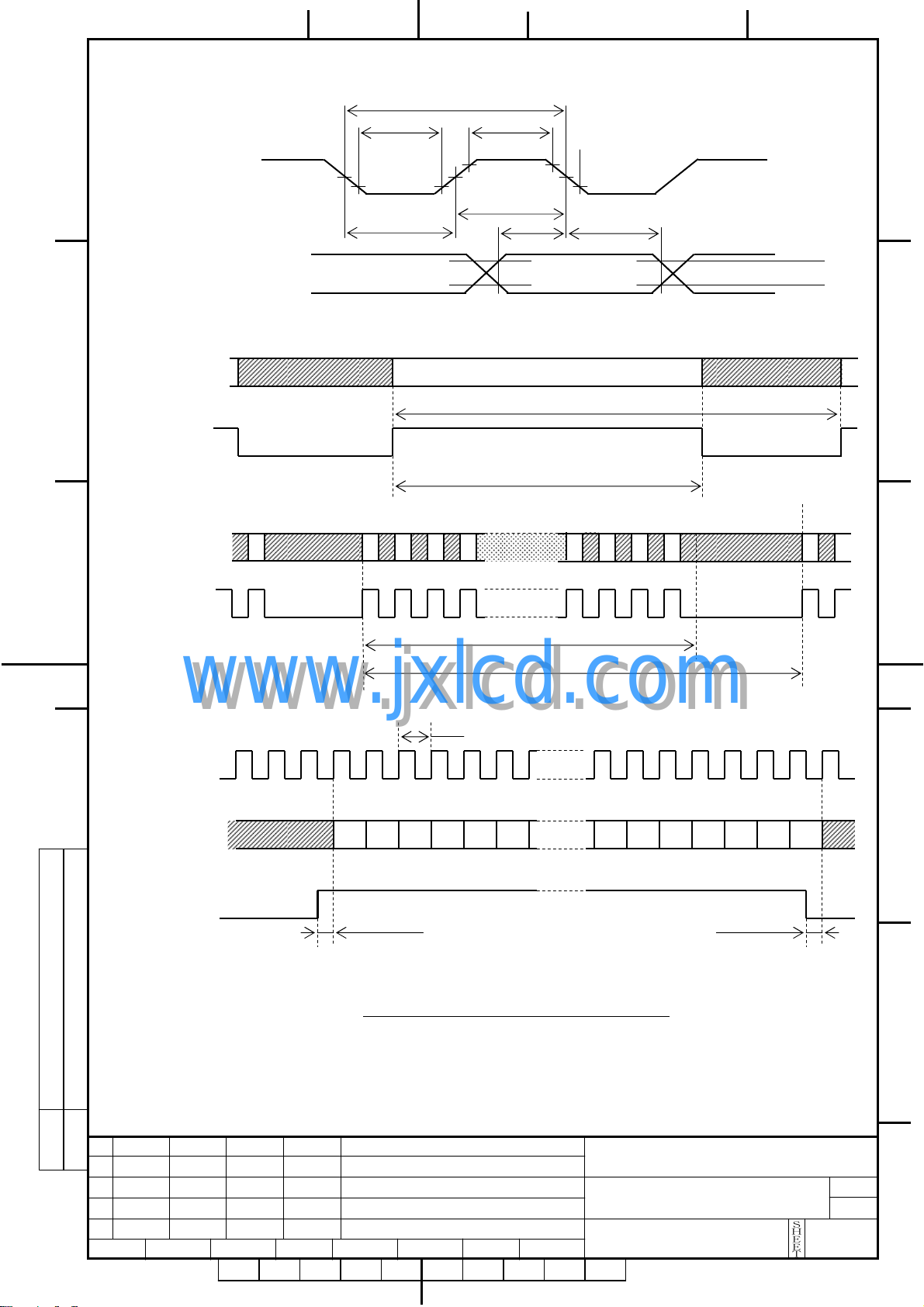
10-4 Input Signal Timing
Table 10-4 and Figure 10-1 shows the Input Signal Timing at LVDS transmitter.
Table 10-4 Timing Characteristics
A
Item Symbol Min. Typ. Max. Unit Remark
Period
DCLK
signal
(Clock)
DCLK-Data
Timing
B
ENAB
signal
Frequency
Duty
High time
Low time
Setup time
Hold time
Hor. Period (1)
Hor. Period (2)
Hor. Display period
Vertical Period
Ver. Frequency
Ver. Di s pl a y p eri od
Data-ENAB timing Tdn — 0 — DCLK *3
(Ta=0~50˚C, Vcc=5±0.25V)
Tc
1/Tc
Tch/ Tc
Tclk H
Tclk L
Tset
Thold
Th
Th
Thd
Tv
1/Tv
Tvd
14.3
40
45
5.0
5.0
3
5
5350/Tc+435
648
640
1028
50
1024
*1
18.5
54
50
—
—
—
—
844
—
640
1066
60
1024
25.0
70
55
—
—
—
—
887
1023
640
1088
76.2
1024
*1
*1
ns
MHz
%
ns
ns
ns
ns
DCLK
DCLK
DCLK
Th
Hz
Th
LVD S Tr
spec.
Tc=n s
*4
*2
16.67ms
*2
*1)•horizontal display position is specified by the rise of ENAB.
The data latched at falling edge of DCLK after rise of ENAB is displayed at the left edge of
the display area.
•Vertical display position is specified by the rise of ENAB after low level continuation over
C C
2048 DCLK.
The data latched at the rise of ENAB is displayed at the top line of the display area.
*2)•If the “High” level period of ENAB is less than 640 DCLK or the number of ENAB in a frame
period (Tv) is less than 1024, black color is displayed at the rest of the display area.
*3)•If ENAB does not synchronize with the effective display data, the display position does not fit
www.jxlcd.com
www.jxlcd.com
to the display area.
*4)•Hor. Period (2) shows the operating range where internal circuit can work correctly.
・When ENAB signal is out of Hor. Period (1), the display quality may deteriorate.
D
D
E
DATE DOCUMENT CONTROL SECTION
EDIT
DESIG.
DATE
DESIG. DESCRIPTION
CHECK
APPR.
CHECK
APPR.
TITLE
DRAW. NO.
SHARP CORPO
SHARP CORPORATIO
SHARP CORPORSHARP CORPO
LQ190E1LX31
(FLC48SXC8V-12)
LD17426
ATION
ATIONATIO
CUST.
SHEET
16
/
1
Page 19
N
N
TclkL
0.9V
A
DCLK
Tc1 Tset
ENAB
RO7-0, RE7-0
GO7-0, GE7-0
BO7-0, BE7-0
B
RO7-0, RE7-0
GO7-0, GE7-0
BO7-0, BE7-0
ENAB
RO7-0, RE7-0
C001 C1024
GO7-0, GE7-0
BO7-0, BE7-0
C C
ENAB
www.jxlcd.com
www.jxlcd.com
DCLK
D
RO7-0, RE7-0
0001
0005
0003
GO7-0, GE7-0
BO7-0, BE7-0
0002
0006
0004
ENAB
Tdn Tdn
Figure 10-1 Input Signal Timing Chart
Tc
0007
0008
Tc
2.3V
0009
0010
Tclk
Tch
Tv
Tvd
0011
0012
1.65
Thd
Thold
Th
1267
1268
1269
1270
1273 1277
1271
1274
1272
1275
1276
2.3V
0.9V
1279
1278
1280
D
E
DATE DOCUMENT CONTROL SECTION
EDIT
DESIG.
DATE
DESIG. DESCRIPTION
CHECK
APPR.
CHECK
APPR.
TITLE
DRAW. NO.
LQ190E1LX31
(FLC48SXC8V-12)
LD17426
SHARP CORPO R ATION
SHARP CORPO R ATIO
SHARP CORPO R ATIONSHARP CORPO R ATIO
CUST.
SHEET
17
/
1
Page 20
N
N
10-5 Correspondence between Data and Display Position
Figure 10-2 shows the C orres pondence between Data and Display Position.
A
C001
S0001 S0002 S0003 S0004 S0005 S0006 S0007
RO
0001
GO
0001
BO
0001
RE
0002
GE
0002
BE
0002
RO
0003
GO
0003
B
C1024
RO
0001
GO
0001
BO
0001
RE
0002
GE
0002
BE
0002
RO
0003
GO
0003
Figure 10-2 Correspondence Data and Display Position
C C
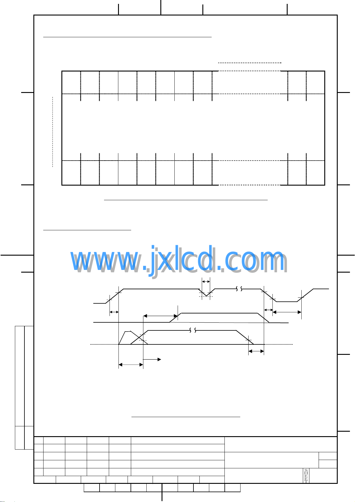
10-6 Power Supply Sequence
The sequence of input signals and On/Off of the power supply of this LCD module
S3839 S3840
GE
1280
GE
1280
BE
1280
BE
1280
should be in the specification s hown in Figure 10-3 to prevent latch-up of t he
driver ICs and DC driving of t h e LCD panel.
Vcc
D
PD
LVDS
Differential
*Note : PD input can be set open, if it is not used.
www.jxlcd.com
Input
www.jxlcd.com
ON
OFF
(0V)
H
L
Tri-state
4.75V
T1≦20ms
T2
0ms≦T2≦40ms
Inputs should be in a range of the spec. of the LVDS.
0ms≦T3
90%
10%
DCLK should be in a range of
the spec.(Frequency etc.)of
the LCD.
T4≦20ms(Voltage descent)
4.75V
(4.5V)
T6≦20ms
2.0V
~
~
~ ~
4.75V
0.5V
0.5s≦T7
Tri-state
0ms≦T5≦40ms
0.5V
D
E
Figure 10-3 Power Supply Sequence
DATE DOCUMENT CONTROL SECTION
EDIT
DESIG.
DATE
DESIG. DESCRIPTION
CHECK
1
APPR.
CHECK
APPR.
TITLE
DRAW. NO.
LQ190E1LX31
(FLC48SXC8V-12)
LD17426
SHARP CORPO R ATION
SHARP CORPO R ATIO
SHARP CORPO R ATIONSHARP CORPO R ATIO
CUST.
SHEET
18
/
Page 21
N
N
11. BACK
11. BACK----LIGHT SPECIFICATIONS
11. BACK11. BACK
LIGHT SPECIFICATIONS
LIGHT SPECIFICATIONSLIGHT SPECIFICATIONS
11- 1 Pin configuration for Back-light
A
Table 11-1 Pin Assignment of CN-A to CN-F
B
11-2 Life
C C
D
Ta ble 11-1 shows the description and Pin assignment of the connectors
(CN-A to F) for the Back- lig ht of t his LCD module.
Pin
№
Connector : Housing : BDBR-03(4.0)V-S
User’s Connector : Post with base : SM02(8.0)B-BDBS-1 or SM02(8.0)B-BHS-1-TB
Supplier : Japan Solderless Terminal Trading Company LTD. (J.S.T.)
(1) Working conditions
(2) Definition of life
CN-A CN-B CN-C CN-D CN-E CN-F
V
1
2 — — — — — — — —
3 GND GND GND GND GND GND Ground Aqua, White, Black
The life of the back-light is a minimum of 50,000 hour s at t he f ollowing conditions.
①Ambient temperature: 25±5℃
②Tube current (I
www.jxlcd.com
①Brightness become s 50% or less than the minimum brightness value s hown in Table 9-1.
②The lamp cannot be lit by the minimum val ue of the breakdown voltage(1760Vrms)
shown in Table 8-1.
③Flashing.
V
1
L
www.jxlcd.com
V
2
L
) : 7mA or less
L
Signal Function Cable color
V
3
L
Contact : SBH-001T-P0.5 (Pin No.1:All signal)
③SPHD-002T-P0.5 (Pin No.3:All signal)
V
4
L
V
5
L
Power supply
6
L
Pink, Red, Orange
11-3 Lamp assembly set (for repla cem ent)
Lamp assembly set(with charge)is prepared for replacing old lamp to new one.
DATE DOCUMENT CONTROL SECTION
05
03 20041125 Add contact of connector.
EDIT
DESIG.
This set consists of a upper lamp assembly and a l o w er lamp assembly.
Type number : LQ0DDB5468(FLCL-40)
Minimum order qty. unit : 20 pcs.
20050420 Lamp Assy No. was changed.
DATE
DESIG. DESCRIPTION
CHECK
1
APPR.
CHECK
APPR.
TITLE
DRAW. NO.
SHARP CORPO R ATION
SHARP CORPO R ATIO
SHARP CORPO R ATIONSHARP CORPO R ATIO
LQ190E1LX31
(FLC48SXC8V-12)
LD17426
SHEET
19
/
D
E
CUST.
Page 22
N
N
12. APPEARANCE SPECIFICA TIONS
12. APPEARANCE SPECIFICA TIONS
12. APPEARANCE SPECIFICA TIONS12. APPEARANCE SPECIFICA TIONS
12-1 Appearance
A
No. Item Judgment method and standard
1 Bright spot (high and Low) <4 dots (Note 1 )
2 Bright spot connection
(high and low)
3 T otal of bright spot <4 dots
4 Dark spot <8 dots (Note 2)
5 Dark spot connection
B
C C
D
6 T otal of dark spot <8 dots (Note 2)
7 Total of dot defect
(bright and dark)
8 high-hgh >15mm
Distance of
bright spot
9 Distance of dark spot > 5mm
10
Scratch on polarizer,
line shape
11
Dent on polarizer,
dot shape
www.jxlcd.com
12
13
14
15
www.jxlcd.com
Bubble in polarize r
Black white spot
(Foreign circular matter)
Light leakage by foreign
articles
Lints,
black/white line
<2 pair (Note 1)
(2 dot connection in horizontal only)
3 pairs (Note 2)
<
8 dots
<
others > 5mm
W<0.03 ―――― Ignore
L≤6
0.03<W<0.05
0.05<W<0.10
0.10<W ―――― 0
D≤0.3
0.3<D<0.4 <5
0.4<D 0
D<0.3 Ignore
0.3<D<0.5 <5
0.5<D 0
D<0.3 Ignore
0.3<D<0.5 <5
0.5<D 0
D<0.3 Ignore
0.3<D<0.6 <4
0.6<D 0
W<0.03 ―――― Ignore
0.03<W<0.05
0.05<W<0.10
0.10<W (W+L)/2=D Conform to No.13
6<L<12 <5
12<L 0
L<0.6 Ignore
0.6<L 0
L≤6
6<L<12 <4
12<L 0
L≤0.6
0.6<L<5 <2
5<L 0
Ignore
Ignore
Ignore
Ignore
D
E
16 Mura
D:Average diameter [mm], W:Width [mm], L:Length [mm], S=(bright spot size)/(dot size)
EDIT
DESIG.
DATE
DESIG. DESCRIPTION
CHECK
1
APPR.
CHECK
DATE DOCUMENT CONTROL SECTION
Invisible under 6% ND filter from ce nter of d is pl ay.
(Display pattern : Black, White, 50% gray)
APPR.
TITLE
DRAW. NO.
SHARP CORPO R ATION
SHARP CORPO R ATIO
SHARP CORPO R ATIONSHARP CORPO R ATIO
LQ190E1LX31
(FLC48SXC8V-12)
LD17426
SHEET
20
CUST.
/
Page 23

N
N
12-2 Dot defects (Bright spots, Dark spots)
A
12-2-1 Zone
· Inside display dot are a (376. 32×301.056mm)
· Display dot area means active area.
· One pixel consists of 3 dots (red, green and blue).
· Foreign particle and scratch unharmful to display image, such as the foreign particle
under polarizer film but outside of the display area and scratch on metal bezel, backlight
module or polarizer film out of the display are a, etc. , are not counted.
B
12-2-2 Bright spots
(1) Bright spots by the defect of TFT.
· Visible under bias of 2% ND filter ...................................High bright spot R•G
· Visible under 5% but invisible under 2% ND filter........Low bright spot R•G•B
C C
· Invisible under bias of 5% ND filter................................Not counted
(2) Bright spots by the light passing through tears, breaks, etc in color filter.
· Exceed size of a half dot ...................................................High bright spot
· A half dot or less................................................................Not counted
(3) Bright spots by the light passing through tears, breaks, etc in chromium mask.
· Exceed 50µm......................................................................High bright spot
· 50µm or less .....................................................................Not counted
D
12-2-3 Test condition
(Note1) Please do not mistake a single bright spot for a bright spot connection due to
(Note2) If a pixel is dark partially, it connects into the number of dark spots in accordance with
www.jxlcd.com
www.jxlcd.com
· Inspector must observe the LCD screen from the normal direction under the illu mination by
a single 20W fluorescent lamp. The distance between the LCD screen and the inspector
should be a height of 50cm above the wor k table.
The vertical illumi nance is 300 to 600lux (reference value) .
· Bright spot should be counted under entire black screen.
· Dark spot should be counted under entire white screen.
· Input signal timing should be typical value.
Cs(supplemental capacitance) line at the center of each dot.
following rule.
(a) A<1/3 : Not count. Only one of 4 dark connection is allowed.
(b) 1/3<
(c) 2/3<
A<2/3 : Considered as 0.5 dot.
A : Considered as 1 dot.
(A=Dark spot size/dot size)
D
E
DATE DOCUMENT CONTROL SECTION
EDIT
DATE
DESIG.
DESIG. DESCRIPTION
CHECK
1
APPR.
CHECK
APPR.
TITLE
DRAW. NO.
SHARP CORPO R ATION
SHARP CORPO R ATIO
SHARP CORPO R ATIONSHARP CORPO R ATIO
LQ190E1LX31
(FLC48SXC8V-12)
LD17426
CUST.
SHEET
21
/
Page 24
N
N
(
)
(
)
)
13. ENVIRONMENTAL SPECIFICAT IONS
13. ENVIRONMENTAL SPECIFICAT IONS
13. ENVIRONMENTAL SPECIFICAT IONS13. ENVIRONMENTAL SPECIFICAT IONS
A
B
C C
Ta ble 13-1 show the environmental specificat ions.
Table 13-1 Environmental specifications
Item Condition Remark
Operation
Temperature
Storage –20~60ºC
Operation
Humidity
Storage 5~85%RH
10~500Hz, 1octave/ 20minute,
Vibration Non-operation
Shock *1 Non-operation
NOTE: Table 13-2 and Fig ure 13-1 show the shock resistance stan dard when module is packaged.
19.6m/s
1hour each X, Yand Z directions.
294m/s
each ±X, ±Y and ±Z directions.
0~55
20~85%RH
2
(2G), 1.5mm max,
2
(30G), 6ms, 1time
50℃
Temperature on surface of
LCD panel (display area.)
Maximum wet-bulb temperature
should not exceed 29ºC.
No condensation.
For single module
without package.
D
Table 13-2 Shock resist ance standard when module is packaged
Dropping location Dropping height Count
www.jxlcd.com
www.jxlcd.com
F (Side face)
A~J 60cm 1 time
G (Top face) J
I
Front face)
Figure 13-1 Direction to apply shock to package
D (Edge) H (Bottom face
Rear face
C (Edge)
E (Side face)
B (Edge)
A (Corner
D
E
DATE DOCUMENT CONTROL SECTION
02 20040826 Correction of temperature.
EDIT
DATE
DESIG.
DESIG. DESCRIPTION
CHECK
1
APPR.
CHECK
APPR.
TITLE
DRAW. NO.
SHARP CORPO R ATION
SHARP CORPO R ATIO
SHARP CORPO R ATIONSHARP CORPO R ATIO
LQ190E1LX31
(FLC48SXC8V-12)
LD17426
CUST.
SHEET
22
/
Page 25

N
N
14. INDICATIONS
14. INDICATIONS
14. INDICATIONS14. INDICATIONS
A
This module has th e f ollowing indications.
(1) Product name : LCD
(2) SHARP Model Number : LQ190E1LX31
(3) Model Number : FLC48SXC8V-12
LCD unit
unit
LCD LCD
unitunit
(4) Manufacturing Number : 5
B
(5) Version number : 01A
C C
D
(6) Manufacturer Country Name :
(7) Company Name : SHARP CORPORATION
(8) Disposal method of cold-cathode tubes.
(9) Caution when changing cold-cat hode tubes.
15. PACKAGING
15. PACKAGING
15. PACKAGING15. PACKAGING
15-1 Packing specifications
www.jxlcd.com
www.jxlcd.com
(1) 5 LCD modules/1package.
LCD unit MADE IN ******
FLC48SXC8V -12 5600001
LQ190E1LX31 01A
SHARP CORPORATION
Figure 14-1 Product Label (Example)
5 6666 0 0 0 0 1
0 0 0 0 1
5 5
0 0 0 0 1 0 0 0 0 1
Serial number
(To be reset every month on 1st.)
Manufacturing month
(Oct. = X, Nov. =Y, Dec. =Z)
Last digit of manufacturing year .
01A (Example)
01A01A
-1st 2 digits “01” means operation al version.
-3rd alphabet means function al version.
Bar code
D
(2) Weight : ap proximately 16kg /1package.
(3) Outline dimensions: 499mm (W)x 250mm (D)x 464mm (H)
15-2 Packing method
Figure 15-2 show the pack ing method.
DATE DOCUMENT CONTROL SECTION
20050420 Model name and Company Name was changed.
05
EDIT
DATE
DESIG.
DESIG. DESCRIPTION
CHECK
1
APPR.
CHECK
APPR.
TITLE
DRAW. NO.
SHARP CORPO R ATION
SHARP CORPO R ATIO
SHARP CORPO R ATIONSHARP CORPO R ATIO
LQ190E1LX31
(FLC48SXC8V-12)
LD17426
SHEET
23
/
E
CUST.
Page 26

N
N
A
B
C C
Put the cable in slot
Front side
Rear side
Protective sheet
D
www.jxlcd.com
www.jxlcd.com
Anti-Electric Bag
D
Front side
E
Fig.15-2 (a) Packaging Method
DATE DOCUMENT CONTROL SECTION
EDIT
DESIG.
DATE
DESIG. DESCRIPTION
CHECK
1
APPR.
CHECK
APPR.
TITLE
DRAW. NO.
SHARP CORPO R ATIO
SHARP CORPO R ATION
SHARP CORPO R ATIONSHARP CORPO R ATIO
LQ190E1LX31
(FLC48SXC8V-12)
LD17426
CUST.
SHEET
24
/
Page 27

N
N
Partition Box
Anti-
A
B
C C
①
①
①①
②
②
②②
LCD Unit
Electrostatic bag
Holder
④
④
③
③
③③
www.jxlcd.com
www.jxlcd.com
D
●Cautious● The bending direction should
Do not to put Anti-electrostatic bag be arranged.
in the partition box.
④④
D
E
DATE DOCUMENT CONTROL SECTION
EDIT
DESIG.
DATE
DESIG. DESCRIPTION
CHECK
1
APPR.
CHECK
APPR.
TITLE
DRAW. NO.
SHARP CORPO R ATIO
SHARP CORPO R ATION
SHARP CORPO R ATIONSHARP CORPO R ATIO
LQ190E1LX31
(FLC48SXC8V-12)
LD17426
CUST.
SHEET
25
/
Page 28

A
N
N
B
⑤
⑤
⑤⑤
The Front side of LCD units
should be faced to the direction of
the making on carton box.
⑥
⑥
⑥⑥
Holder
⑧
⑧
⑦
⑦
⑦⑦
C C
www.jxlcd.com
www.jxlcd.com
Carton Box
D
Sample of carton label
型 格 (TYPE) FLC48SXC8V -12 数 量 (QTY.) 5
図 番(DRG. No.) LQ190E1LX31 版 数(Rev. No.) 01A
5600001
5600002
5600003
5600004
5600005
Bar code
⑧⑧
499
499
499499
250
250
250250
464
464
464464
D
E
Fig.15-2 (b) Packaging Method
DATE DOCUMENT CONTROL SECTION
20050420 Model name was changed.
05
EDIT
DESIG.
DATE
DESIG. DESCRIPTION
CHECK
1
APPR.
CHECK
APPR.
TITLE
DRAW. NO.
SHARP CORPO R ATIO
SHARP CORPO R ATION
SHARP CORPO R ATIONSHARP CORPO R ATIO
LQ190E1LX31
(FLC48SXC8V-12)
LD17426
CUST.
SHEET
26
/
Page 29

N
N
A
B
C C
PP Belt
1532
1532
1532
1532
www.jxlcd.com
www.jxlcd.com
D
Wrap Film (2~3 times wrap)
1000
1000
10001000
Carton Qty./ pallet : 8 boxes×3 layers (maximum 24 boxes)
Fig.15-2 (c) Packaging Method
DATE DOCUMENT CONTROL SECTION
02 20040826 Correction of packing method.
EDIT
DESIG.
DATE
DESIG. DESCRIPTION
CHECK
1
APPR.
CHECK
APPR.
1000
1000
10001000
Conner angle
TITLE
DRAW. NO.
SHARP CORPO R ATIO
SHARP CORPO R ATION
SHARP CORPO R ATIONSHARP CORPO R ATIO
LQ190E1LX31
(FLC48SXC8V-12)
LD17426
D
E
CUST.
SHEET
27
/
Page 30

A
N
N
B
Cushioning ma t erial
602
(580)
Corrugated carton (A)
with LCD modules
Corrugated fiberboard shipping container (B)
C C
Note 1) The carton (A) should be placed in the middle of the contai ner (B) with enough cushioning
Note2) The figures in ( ) show inside measurements of the container (B).
D
446
(430)
materials.
www.jxlcd.com
www.jxlcd.com
646
(630)
Figure.15-2 (d) Packing method
D
DATE DOCUMENT CONTROL SECTION
EDIT
DESIG.
DATE
DESIG. DESCRIPTION
CHECK
1
APPR.
CHECK
APPR.
TITLE
DRAW. NO.
SHARP CORPO R ATIO
SHARP CORPO R ATION
SHARP CORPO R ATIONSHARP CORPO R ATIO
LQ190E1LX31
(FLC48SXC8V-12)
LD17426
SHEET
28
/
E
CUST.
Page 31

N
N
16.WARRANTY
16.WARRANTY
16.WARRANTY16.WARRANTY
The warranty period is one year after shipping. Products which fail during this period are
A
17.PRECAUTIONS
B
C C
repaired or replaced without charge, unless the failure is caused by user.
17.PRECAUTIONS
17.PRECAUTIONS17.PRECAUTIONS
Adhere to the following precautions to u se th is L CD module properly.
(1) Fail safe design
(1) Fail safe design
(1) Fail safe design (1) Fail safe design
LCD module has an inherent chance of failure. Customers must protect a g ainst injury,
damage or loss from such failures by in corporating safety design measures into your
facility and equipment such as redund ancy, fire protection, and prevention of over-current
levels and other abnormal operating conditions.
((((2222) Handling of LCD panel
) Handling of LCD panel
) Handling of LCD panel) Handling of LCD panel
①
① Do not apply any strong mechanical shock to the LCD pane l.
Do not apply any strong mechanical shock to the LCD panel.
①①
Do not apply any strong mechanical shock to the LCD panel. Do not apply any strong mechanical shock to the LCD panel.
Since the LCD panel is made of glass, excessive shock may damage the panel or cause a
malfunction.
②
② Do not press hard on the LCD panel surface.
Do not press hard on the LCD p anel surface.
②②
Do not press hard on the LCD panel surface. Do not press hard on the LCD panel surface.
In the LCD panel, the gap between two glass plates is kept perfectly even to maintain
display properties and reliability. The hard pressure on the LCD panel may cause the
2
following problems. If the pressure is over 2kg/cm
, the problem don’t return to normal
D
condition.
① Ununiformity of color
② Disorder of orient ation of liquid crystal
www.jxlcd.com
Problem ① returns to normal condition after a while. Problem ② returns to normal
www.jxlcd.com
condition by turning the power off and turning on again.
・For handling, use cotton or conductive gloves so that the display surface is not soiled.
・If dust or dirt soils the display surface, clean it as follows with a soft cloth (deerskin, etc.)
However these operations should be avoided to insure reliabi lity.
③
③ Do not scratch the polarizer film on the LCD panel surface.
Do not scratch the polarizer film on the LCD panel surface.
③③
Do not scratch the polarizer film on the LCD panel surface. Do not scratch the polarizer film on the LCD panel surface.
・Do not press or rub the display surface with a hard tool, tweezers, etc.
[Dust] Wipe off with a soft cloth. (do not rub.)
[Dirt ] Apply clear water to a soft cloth and squeeze hard out of water drops, then lightly
wipe off the specified parts. Only if the dirt is hardly wiped off, use isopropyl alcohol
or ethanol.
Be careful not to splash the water or the solvents on the edge of polarizer and in the
LCD unit.
The polarizer possibly exfoliates due to the solvent and water penetrated between
the polarizer and the LCD panel.
D
E
Do not use unspecified solvent such as ketone (acetone, etc.) and aromatics (xylene,
toluene, etc.)
DATE DOCUMENT CONTROL SECTION
EDIT
DATE
DESIG.
DESIG. DESCRIPTION
CHECK
1
APPR.
CHECK
APPR.
TITLE
DRAW. NO.
SHARP CORPO R ATIO
SHARP CORPO R ATION
SHARP CORPO R ATIONSHARP CORPO R ATIO
LQ190E1LX31
(FLC48SXC8V-12)
LD17426
CUST.
SHEET
29
/
Page 32

N
N
(Caution) Be careful not to allow the water or solvent to enter the module.
A
B
C C
D
DATE DOCUMENT CONTROL SECTION
・If saliva or water drops are left for a long period of time, the part may become
deformed or discolored.
Wipe of f im mediately in the same way as for dirt.
・Do not allow oil to adhere to the module since excessive oil is hard to clean.
④
④ Do not place or contact objects on the display surface for a long period of time.
Do not place or contact objects on the display surface for a long period of time.
④④
Do not place or contact objects on the display surface for a long period of time. Do not place or contact objects on the display surface for a long period of time.
This may make some parts of the LCD module distorted and the quality of display may
deteriorate.
((((3333) Ha ndling
) Handling of LCD module
) Handlin g ) Handling
①
① Do not pull the cold
Do not pull the cold----cathode tube cable strongly.
①①
Do not pull the cold Do not pull the cold
If the cable is pulled with the strength of 2kg or more, the cable may be damaged or may
・For assembling the module, operator should be grounded and wear cotton or conductive
gloves.
・Floor of work area and work table to assemble the LCD module should be covered with
electrostatic shielding in order to discharge static electricity via an earth wire.
・Do not take the module out of the conductive bag until the module is assembled.
EDIT
DESIG.
lose reliability.
②
② Assemble the module into user’s system in a dust free environment.
Assemble the module into use r’s system in a dust free enviro nment.
②②
Assemble the module into use r’s system in a dust free enviro nment. Assemble the module into use r’s system in a dust free enviro nment.
Conductive foreign matter adheres to the module may cause failures.
③
③ Take anti
Take anti----electrostatic measures for assembling the module.
③③
Take anti Take anti
Since the LCD module contains CMOS-ICs, the following points should be observed.
・If necessary, ground operation tools (soldering iron, radio pliers, tweezers, etc.).
www.jxlcd.com
・Do not assemble the module under low humidity (50%RH or less).
④
④ Do not pull the connecting cable
Do not pull the connecting cable on the rear face of the LCD module strongly.
④④
Do not pull the connecting cable Do not pull the connecting cable
⑤
⑤ Do not disassemble or remodel the LCD module.
Do not disassemble or remodel the LCD module.
⑤⑤
Do not disassemble or remodel the LCD module. Do not disassemble or remodel the LCD module.
Disassembly or remodeling of the LCD module may result in malfunctions or deterioration
of the display qualit y and reliability.
((((4444) Precautions in regards of ope
) Precautions in regards of operating the LCD module
) Precautions in regards of ope) Precautions in regards of ope
①
①Ad here t o t he specified power supply sequence.
Adhere to the specified powe r sup ply sequence.
①①
Adhere to the specified powe r sup ply sequence.Adhere to the specified powe r sup ply sequence.
If not followed, the CMOS-IC may cause a latch-up, or DC voltage may be applied to the
liquid crystal, whi c h cause a failure or serious deterioration in display qualit y.
②
②Do not operate
Do not operate the LCD module when condensation occurs.
②②
Do not operate Do not operate
If the LCD module is operated when condensation is on the terminals of the LCD panel, the
terminals cause electrochemical reaction, and may reach disconnection. Condensation
easily occurs especially when the module is moved from cold environment to warm
environment.
DATE
DESIG. DESCRIPTION
of LCD module
of LCD moduleof LCD module
cathode tube cable strongly.
cathode tube cable strongly.cathode tube cable strongly.
electrostatic measures for assembling the module.
electrostatic measures for assembling the module.electrostatic measures for assembling the module.
www.jxlcd.com
on the rear face of the LCD module strongly.
on the rear face of the LCD module strongly.on the rear face of the LCD module strongly.
rating the LCD module
rating the LCD modulerating the LCD module
the LCD module when condensation occurs.
the LCD module when condensation occurs.the LCD module when condensation occurs.
LQ190E1LX31
(FLC48SXC8V-12)
LD17426
1
CHECK
APPR.
CHECK
APPR.
TITLE
DRAW. NO.
SHARP CORPO R ATIO
SHARP CORPO R ATION
SHARP CORPO R ATIONSHARP CORPO R ATIO
D
E
CUST.
SHEET
30
/
Page 33
A
N
N
③
③The following troubles occur when the LCD module is not used under recommended
The following troubles occur when the LCD module is not used under recommended
③③
The following troubles occur when the LCD module is not used under recommended The following troubles occur when the LCD module is not used under recommended
temperature.
temperature.
temperature.temperature.
・Operation under high tempe rature(>50℃): Display colors shift to blue.
・Storage under high temperature(>60℃): The polarizer film deteriorates and contrast
B
C C
D
decreases.
・Operation under low temperatur e(< 0℃): The response speed decreases considerably.
・Storage under low temperature(<-20℃): The liquid crystal may solidify and become
damaged.
④
④Be sure to in
Be sure to input the control signals at the correct timing.
④④
Be sure to inBe sure to in
If control signals (DCLK, ENAB) are not input, or if the timing is out of the specified timing,
DC voltage may be applied to the liquid crystal and, as a result, cause image sticking or
deterioration of contrast.
((((5555) Precautions in regards of designing mo dule mounting
) Precautions in regards of desig ning module mounting
) Precautions in regards of desig ning module mounting) Precautions in regards of desig ning module mounting
①
①Excessive force should not be applied to the screen or the rear side of the LCD module.
Excessive force should not be applied to the screen or the rear side of the LCD module.
①①
Excessive force should not be applied to the screen or the rear side of the LCD module.Excessive force should not be applied to the screen or the rear side of the LCD module.
Excessive pressure on the screen caused by the installation of the LCD module may
deteriorate display quality and reliability.
Brightness uniformity and the reliability of CC FL may decrease if the pre ss ure is applied to
the backlight module.
②
②Avoid twisting and bending the LCD module.
Avoid twisting and bending the LCD module.
②②
Avoid twisting and bending the LCD module.Avoid twisting and bending the LCD module.
Excessive twist a nd bend may damage display quality and reliabilit y.
③
③Avoid
Avoid extending the power cable between the LCD module and inverter.
③③
④
④Keep the backlight cable apart from the metal enclosure of the LCD module.
④④
⑤
⑤When
⑤⑤
extending the power cable between the LCD module and inverter.
AvoidAvoid
extending the power cable between the LCD module and inverter. extending the power cable between the LCD module and inverter.
www.jxlcd.com
www.jxlcd.com
This may cause the backlight to flicker or not to light.
Keep the backlight cable apart from the metal enclosure of the LCD module.
Keep the backlight cable apart from the metal enclosure of the LCD module.Keep the backlight cable apart from the metal enclosure of the LCD module.
When frequency current for backlight driving leak to the metal enclosure, the desired
brightness may not be assured.
When mmmmounting LCD module with M
When When
tighten the screws with torque
tighten the screws with torque 3.5kgf.
tighten the screws with torque tighten the screws with torque
put the control signals at the correct timing.
put the control signals at the correct timing.put the control signals at the correct timing.
ounting LCD module with M3
ounting LCD module with Mounting LCD module with M
3 screws (x4),
3 3
3.5kgf.
3.5kgf.3.5kgf.
screws (x4), and rear side [Detail A] M2.5 screws(x2)
screws (x4), screws (x4),
④
and rear side [Detail A] M2.5 screws(x2)
and rear side [Detail A] M2.5 screws(x2)and rear side [Detail A] M2.5 screws(x2)
D
((((6666) Storage method
) Storage method
DATE DOCUMENT CONTROL SECTION
05
04 20050208 Add screw torque.
EDIT
DESIG.
) Storage method) Storage method
①
①Do not store the LCD module in an atmosphere of o
Do not store the LCD module in an atmosphere of organic solvent or corrosive gas.
①①
Do not store the LCD module in an atmosphere of oDo not store the LCD module in an atmosphere of o
In an organic solvent atmosphere, the polarizer film discolors and display quality
deteriorates.
In a corrosive gas environment, various parts of the module may corrode or deter iorate.
②
②Store the LCD module in a
Store the LCD module in a SHARP
②②
Store the LCD module in a Store the LCD module in a
At storing, SHARP packages can be stacked up to 3 boxes.
The LCD module is in an anti-static bag. Keep the module in that status.
20050420 Comp a n y Name was changed
DATE
DESIG. DESCRIPTION
CHECK
1
APPR.
CHECK
SHARP pack
SHARPSHARP
package.
pack pack
age.
age.age.
APPR.
rganic solvent or corrosive gas.
rganic solvent or corrosive gas.rganic solvent or corrosive gas.
TITLE
DRAW. NO.
SHARP CORPO R ATIO
SHARP CORPO R ATION
SHARP CORPO R ATIONSHARP CORPO R ATIO
LQ190E1LX31
(FLC48SXC8V-12)
LD17426
E
CUST.
SHEET
31
/
Page 34

A
N
N
B
③
③The LCD module is recommended to be stored in humidity controlled, cool and dark
The LCD module is recommended to be stored in humidity controlled, cool and dark
③③
The LCD module is recommended to be stored in humidity controlled, cool and dark The LCD module is recommended to be stored in humidity controlled, cool and dark
locations.
locations.
locations.locations.
Recommended storage environment
・Place : Dark (avoid direct sunlight)
・Temperature : 10〜35℃
・Humidity : 50〜60%RH
Note) If the module is left in an environment of 60℃ and above for a long period of time,
optical characteristics may deterior ate.
((((7777) Disposal Method
) Disposal Method
) Disposal Method) Disposal Method
①
① LCD module
LCD module
①①
LCD module LCD module
The components of this LCD module can be grouped into metal, resin, glass and so on. As
the backlight contains CCFL which includes mercury, it must be disposed according to the
(8)
(8) CAUTION IN DESIGNING INVERTER
(8) (8)
local ordinance or regulation s.
②
② Package
Package
②②
Package Package
All the packages are made of recyclable papers except the anti-ESD bag.
CAUTION IN DESIGNING INVERTER
CAUTION IN DESIGNING INVERTERCAUTION IN DESIGNING INVERTER
Fluorescent lamps driven by high voltage are included in this LCD module. Please stand
C C
D
to the instructions be low when designing inverter t hat lights the fluorescent lamps.
Otherwise it may lead to FATAL FAILURE, such as SMOKING or FIRING.
①
① APPLY PROTECTIVE CIRCUIT
APPLY PROTECTIVE CIRCUIT in preparation for lamp breaking, wire breaking and
①①
APPLY PROTECTIVE CIRCUIT APPLY PROTECTIVE CIRCUIT
short circuit. The protective circuit should also detect half open circuit and wire breaking
www.jxlcd.com
www.jxlcd.com
in narrow gap etc.. Ot herwise it may lead to fatal fa il ure.
②
② KEEP ENOUGH CURRENT CAPACITY
KEEP ENOUGH CURRENT CAPACITY of inverter output for leakage current, which
②②
KEEP ENOUGH CURRENT CAPACITY KEEP ENOUGH CURRENT CAPACITY
leaks from lamps and wire to surrounding metal material. Usually output current of
about 1.5 times as same as the lamp current is necessary. But it sometimes varies due to
characteristics of the inverter itself. So before determining design, please check
characteristics of the inverter by connecting it to the LCD module.
③
③ KEEP ENOUGH TEMPERATURE MARGIN
KEEP ENOUGH TEMPERATURE MARGIN for each parts mounted on inverter.
③③
KEEP ENOUGH TEMPERATURE MARGINKEEP ENOUGH TEMPERATURE MARGIN
Temperature of the parts becomes higher when they are mounted in the final products
D
due to heating inside. The temperature of each parts MUST NOT increase over the
guaranteed temperature.
DATE DOCUMENT CONTROL SECTION
EDIT
DESIG.
DATE
DESIG. DESCRIPTION
CHECK
1
APPR.
CHECK
APPR.
TITLE
DRAW. NO.
SHARP CORPO R ATIO
SHARP CORPO R ATION
SHARP CORPO R ATIONSHARP CORPO R ATIO
LQ190E1LX31
(FLC48SXC8V-12)
LD17426
SHEET
32
/
E
CUST.
Page 35
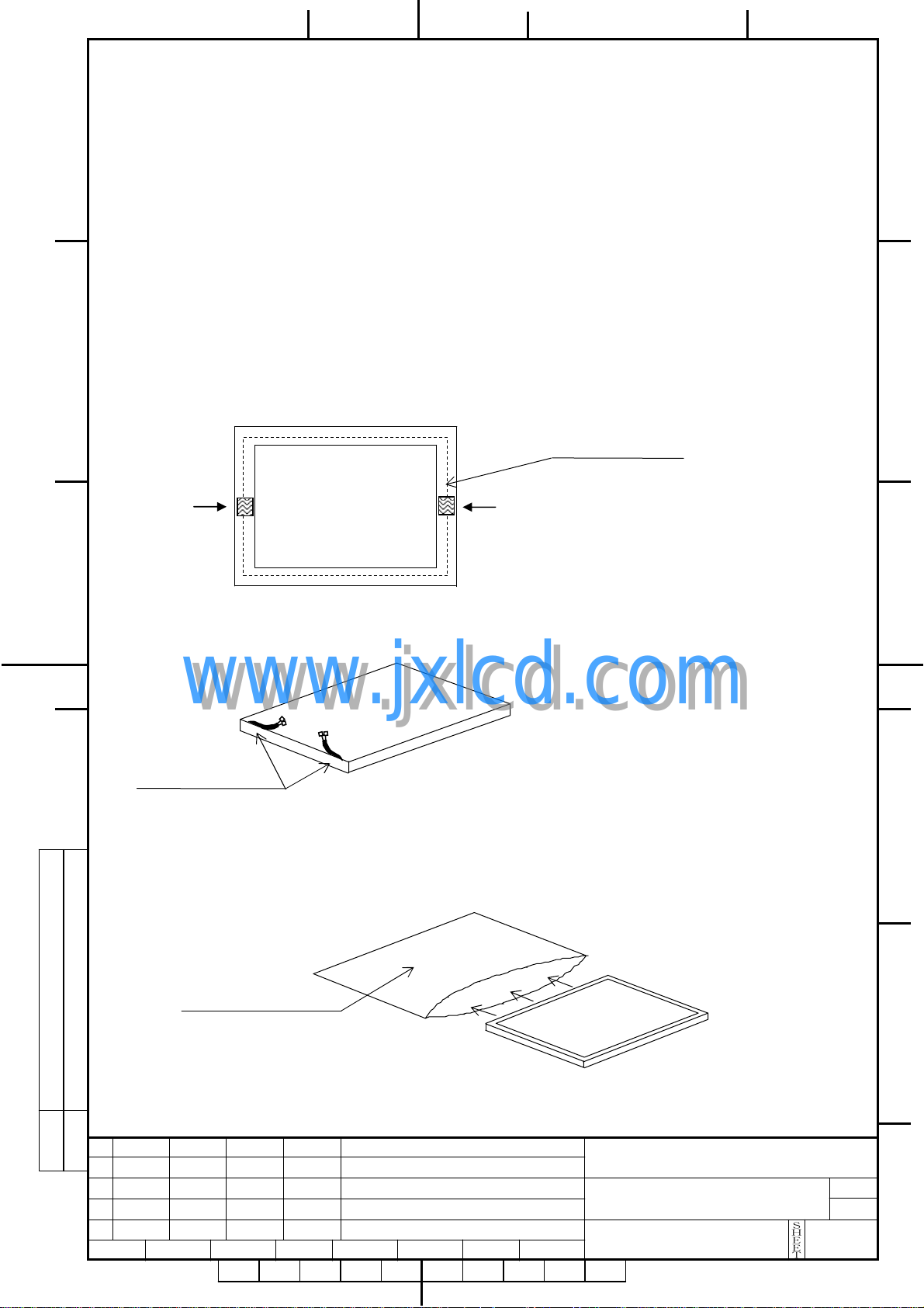
N
N
((((8888))))Return method of the LCD module requested for repair or
Return method of the LCD module requested for repair or analysis
Return method of the LCD module requested for repair or Return method of the LCD module requested for repair or
analysis of the prob
analysisanalysis
of the problem
of the prob of the prob
lem
lemlem
A
B
C C
・When returning the LCD modules, adhere to the following procedures not to damage the LCD
panel or the backlight cables. (Fig. 17-1(a)~(b))
When the LCD module is returne d without following the specified packagin g procedures,
SHARP will not take responsibility for the damages caused by the failure of the packaging
method.
・Please be cautious not to put fingerpri nts or other stains on the display by
wearing a glove or fingerstall when managing LCD module modules, including
faulty modules that require to be returned .
(1) Attach protective sh eet.
Tape
Front side
Protective sheet
(Please tape the sheet onto the frame)
Tape
(2) Put the backlight cables in slots.
www.jxlcd.com
D
Backlight cable
(3) Put the LCD module into the anti-electrostatic bag
(Please do not use torn anti-electrostatic bags)
www.jxlcd.com
Anti-electrostatic bag
Rear side
* If the cables are not fixed, the connectors
may scratch the LCD panel surface or the
cables may be damaged.
Front side
D
E
Fig. 17-1(a) Packaging method
DATE DOCUMENT CONTROL SECTION
20050420 Comp a n y Name was changed
05
EDIT
DATE
DESIG.
DESIG. DESCRIPTION
CHECK
1
APPR.
CHECK
APPR.
TITLE
DRAW. NO.
SHARP CORPO R ATIO
SHARP CORPO R ATION
SHARP CORPO R ATIONSHARP CORPO R ATIO
LQ190E1LX31
(FLC48SXC8V-12)
LD17426
CUST.
SHEET
33
/
Page 36

N
N
(4) Storage into the carton box
A
・When using the carton box manufactured by SHARP
(Please use carton boxes and arrowheads that are not collapsed)
Partition Box
Anti-
②
②
①
①
①①
B
C C
②②
LCD Unit
Electrostatic bag
Holder
www.jxlcd.com
www.jxlcd.com
④
④
③
③
③③
D
●Cautious● The bending direction should
Do not to put Anti-electrostatic bag be arranged.
in the partition box.
④④
D
E
DATE DOCUMENT CONTROL SECTION
05
EDIT
20050420 Comp a n y Name was changed
DATE
DESIG.
DESIG. DESCRIPTION
CHECK
1
APPR.
CHECK
APPR.
TITLE
DRAW. NO.
SHARP CORPO R ATIO
SHARP CORPO R ATION
SHARP CORPO R ATIONSHARP CORPO R ATIO
LQ190E1LX31
(FLC48SXC8V-12)
LD17426
CUST.
SHEET
34
/
Page 37
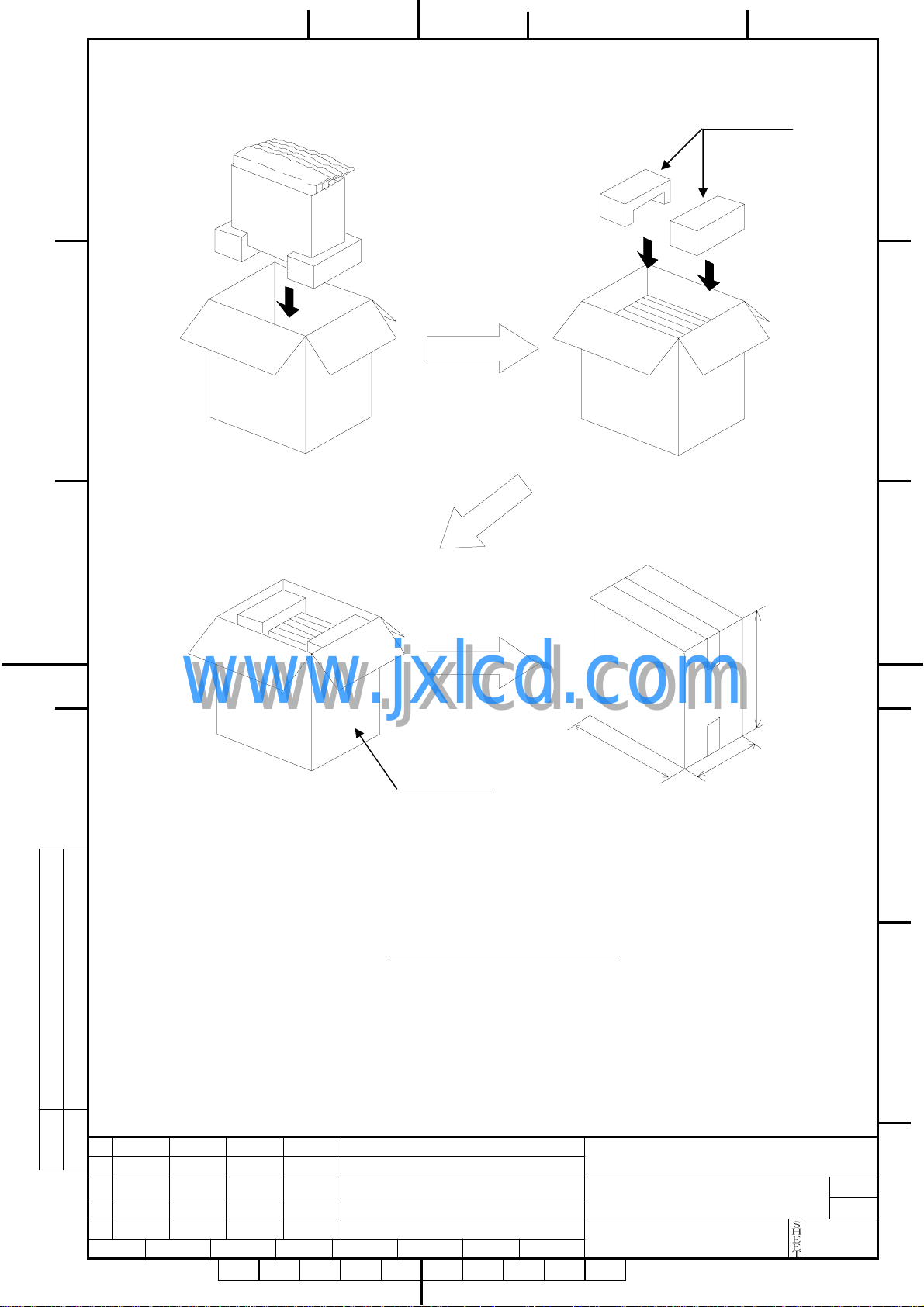
A
N
N
B
⑤
⑤
⑤⑤
The Front side of LCD units
should be faced to the direction of
the making on carton box.
⑥
⑥
⑥⑥
Holder
⑧
⑧
⑦
⑦
C C
D
⑦⑦
www.jxlcd.com
www.jxlcd.com
Carton Box
**The arrowheads are shown on the holders.**
Fig. 17-1(b) Packaging method
・When not using the carton box manufactured by SHARP
Please pack the LCD modules one by one and make sure not to damage the LCD modules
⑧⑧
464
464
464464
499
499
499499
250
250
250250
D
E
when transporting.
DATE DOCUMENT CONTROL SECTION
20050420 Comp a n y Name was changed
05
EDIT
DATE
DESIG.
DESIG. DESCRIPTION
CHECK
1
APPR.
CHECK
APPR.
TITLE
DRAW. NO.
SHARP CORPO R ATIO
SHARP CORPO R ATION
SHARP CORPO R ATIONSHARP CORPO R ATIO
LQ190E1LX31
(FLC48SXC8V-12)
LD17426
CUST.
SHEET
35
/
Page 38

N
N
((((9999) Others
) Others
) Others ) Others
①
①If the LCD
If the LCD panel is damaged, do not in hale and do not swallow the liquid cry st al.
①①
If the LCDIf the LCD
A
18. PRECAUTIONS FOR USE
18. PRECAUTIONS FOR USE
18. PRECAUTIONS FOR USE 18. PRECAUTIONS FOR USE
B
If the liquid crystal adhere to the body or cloths, wash it off with soap immediately.
Follow regular precautio ns for el ectronic components.
②
②Flux residue on the printed circuit board
Flux residue on the printed circuit board is harmless to the quality and reliability of LCD
②②
Flux residue on the printed circuit boardFlux residue on the printed circuit board
module.
module.
module.module.
SHARP has a dopted non-wash tec hnology on module asse m b ly process.
This Product is designed, devel o ped and manufactur ed as contemplate d f o r general use,
including without limitat ion, gen eral office use, personal use, househol d us e, and ordinary
industrial use, but is not designed, developed and manufactured as co nt e mplated for use
accompanying fatal r isks or dangers that, unless extremely high safety is secured, could lead
directly to death, personal injury, severe physical damage or other loss (hereinafter “High
Safety Required Use”), including without limitation, nuclear reaction control in nuclear facility,
aircraft flight control, air traffic control, mass tra ns port co ntrol, medical life support system,
panel is damaged, do not inhale and do not swallow the liqui d cry st al.
panel is damaged, do not inhale and do not swallow the liqui d cry st al. panel is damaged, do not inhale and do not swallow the liqui d cry st al.
is harmless to the quality and reliability of LCD
is harmless to the quality and reliability of LCD is harmless to the quality and reliability of LCD
missile launch cont rol in weapon system. If cust omer’s prod uct possibly falls under th e
category of High Safety Required Use, please consult with our sales representatives in charge
C C
19. MISCELLANEOUS
19. MISCELLANEOUS
19. MISCELLANEOUS19. MISCELLANEOUS
D
before such use. In addition, S HARP shall not be liable against the Customer and/or any third
party for any claims or damages arising in conn ection with the High Safety Required Use of
the Product without permission.
www.jxlcd.com
Specifications of the TFT-LCD panel and other components used in the LC D m odule are
subject to change. Bot h parties shall discus s t og e ther before change.
If any doubt is raised in the content of the specifications, both parties shall discuss and make
best effort for the agreement.
www.jxlcd.com
D
E
DATE DOCUMENT CONTROL SECTION
20050420 Comp a n y Name was changed
05
EDIT
DATE
DESIG.
DESIG. DESCRIPTION
CHECK
1
APPR.
CHECK
APPR.
TITLE
DRAW. NO.
SHARP CORPO R ATIO
SHARP CORPO R ATION
SHARP CORPO R ATIONSHARP CORPO R ATIO
LQ190E1LX31
(FLC48SXC8V-12)
LD17426
CUST.
SHEET
36
/
Page 39
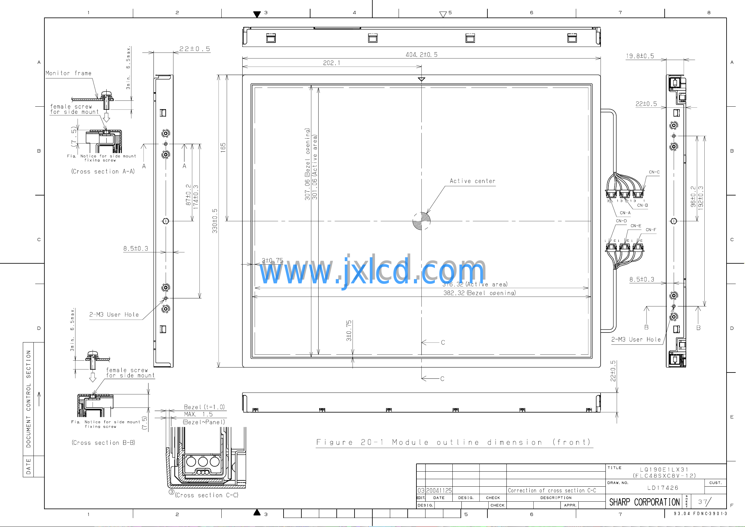
www.jxlcd.com
www.jxlcd.com
Page 40
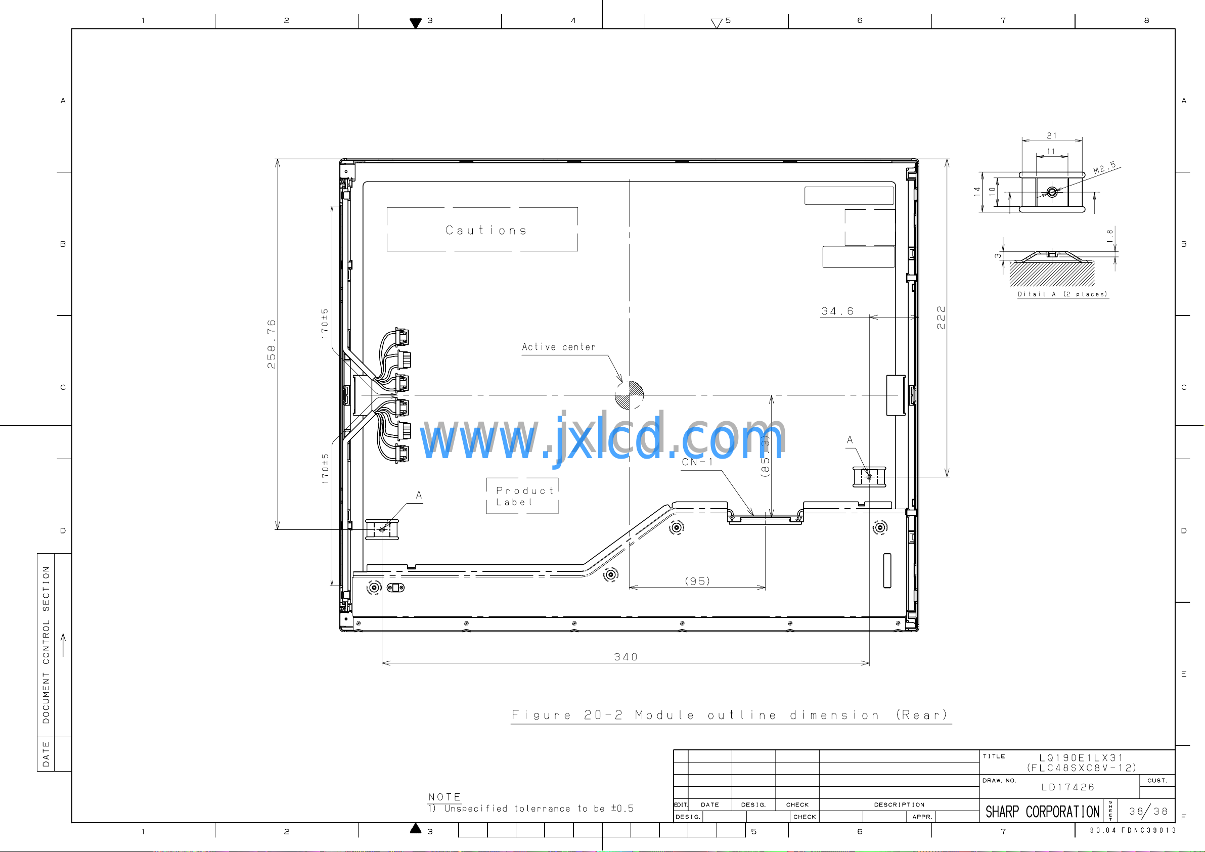
www.jxlcd.com
www.jxlcd.com
 Loading...