

Page 1

Technical Document
LCD Specification
LCD Group
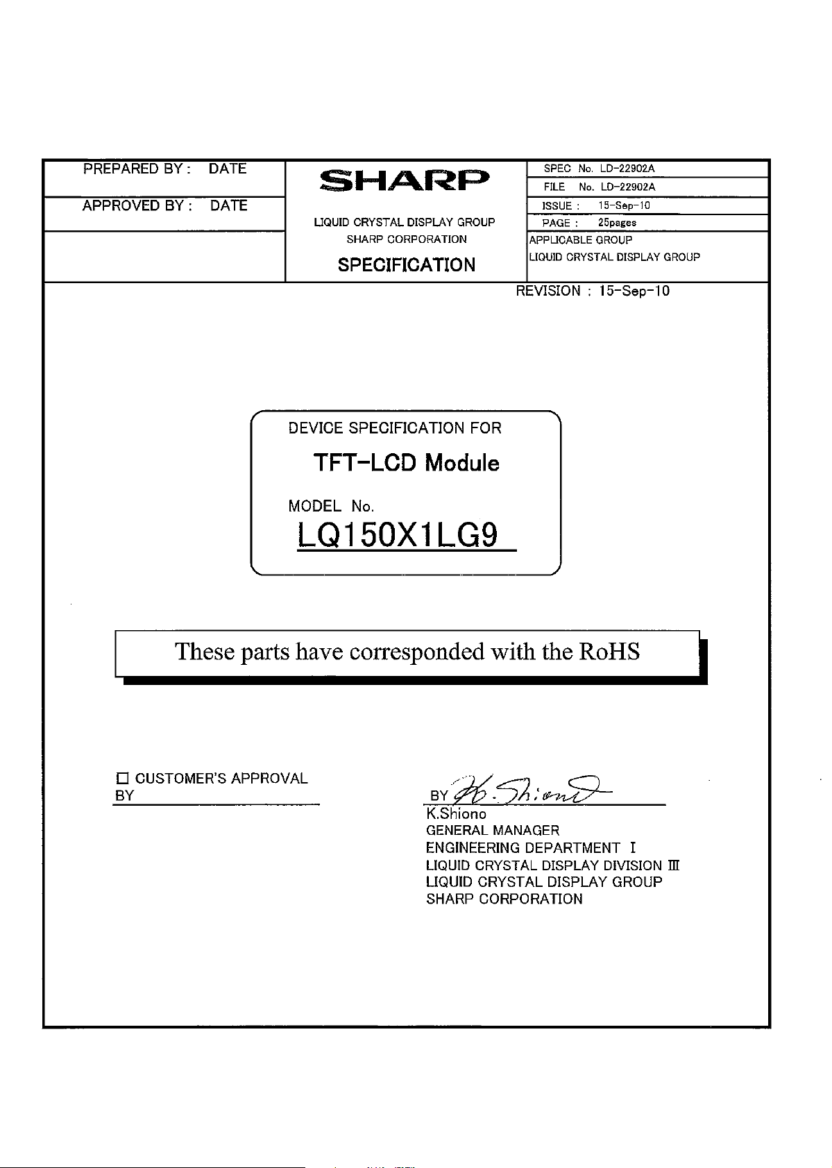
LQ150X1LG93 LCD Module
Product Specification
September 2010
XGA module with True Industrial-rated
LED backlight at 50,000 hours and built-in
backlight driver; high contrast of 800:1
and brightness of 350 nits.
Page 2
3
Page 3
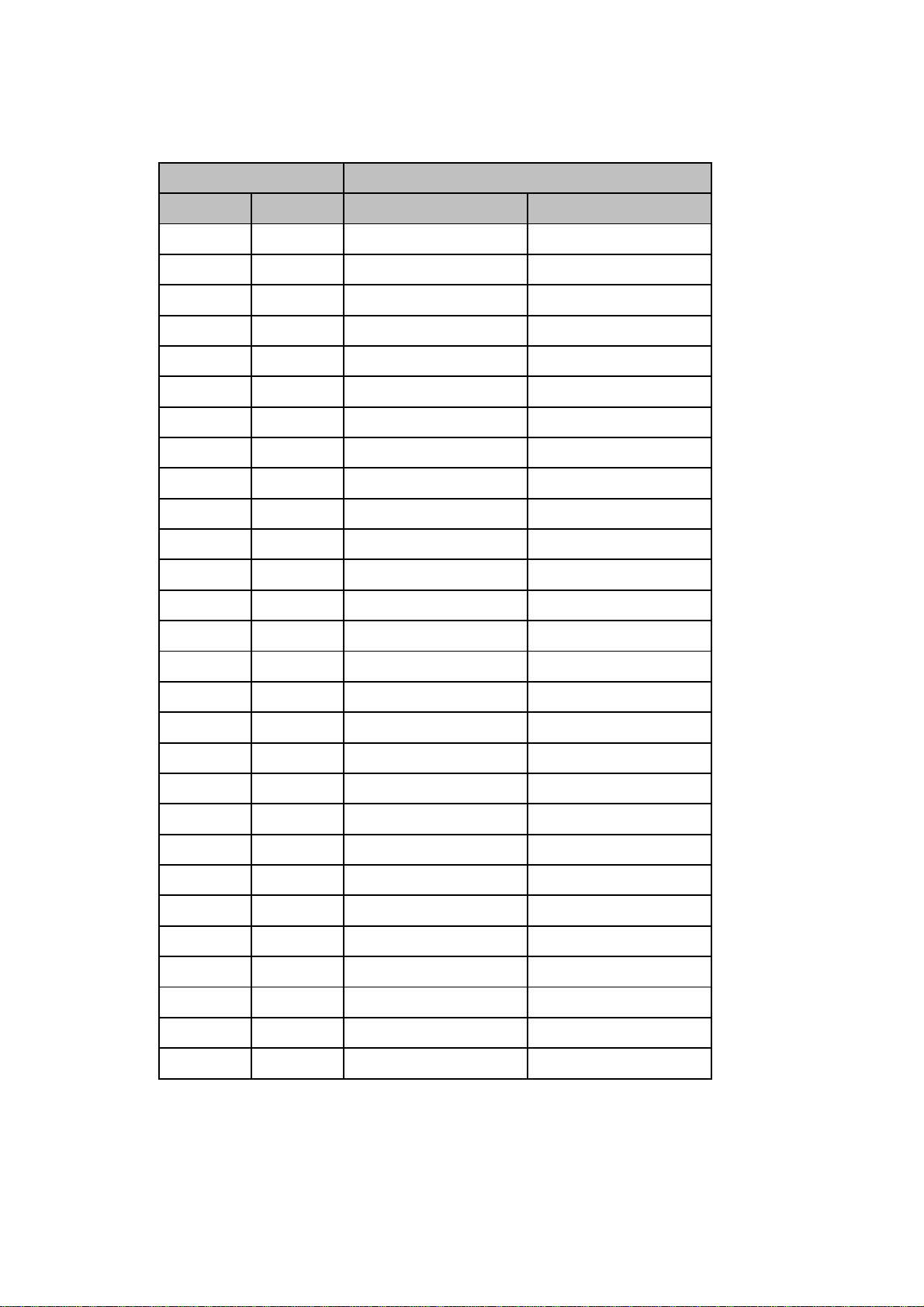
SPEC No.
RECORDS OF REVISION
LQ150X1LG93
DATE SUMMARY
REVI
SED
No
PAGE
NOTE
LD-22902A
2010/9/15 -
Page 4

- Contents -
No. page
1 Application ・・・・・・・・・・・・・・・・・・・・・・・・・・・・・・・・・・・・ 1
2 Overview ・・・・・・・・・・・・・・・・・・・・・・・・・・・・・・・・・・・・ 2
3 Mechanical Specifications ・・・・・・・・・・・・・・・・・・・・・・・・・・・・・・・・・・・・ 2
4 Input Terminals ・・・・・・・・・・・・・・・・・・・・・・・・・・・・・・・・・・・・ 3
5 Absolute Maximum Ratings ・・・・・・・・・・・・・・・・・・・・・・・・・・・・・・・・・ 9
6 Electrical Characteristics ・・・・・・・・・・・・・・・・・・・・・・・・・・・・・・・・・・・・ 10
7 Timing characteristics of input signals ・・・・・・・・・・・・・・・・・・・・・・ 12
8 Input Signals, Basic Display Colors and Gray Scale of Each Color ・・ 13
9 Optical Characteristics ・・・・・・・・・・・・・・・・・・・・・・・・・・・・・・・・・・・・ 15
10 Handling Precautions ・・・・・・・・・・・・・・・・・・・・・・・・・・・・・・・・・・・・ 17
11 Packing form ・・・・・・・・・・・・・・・・・・・・・・・・・・・・・・・・・・・・ 18
12 Reliability test items ・・・・・・・・・・・・・・・・・・・・・・・・・・・・・・・・・・・・ 18
13 Others ・・・・・・・・・・・・・・・・・・・・・・・・・・・・・・・・・・・・ 19
14 Storage conditions ・・・・・・・・・・・・・・・・・・・・・・・・・・・・・・・・・・・・ 20
Fig.1 OUTLINE DIMENSIONS ・・・・・・・・・・・・・・・・・・・・・・・・・・・・・・・・・・・・ 21
Fig.3 PACKING FORM ・・・・・・・・・・・・・・・・・・・・・・・・・・・・・・・・・・・・ 22
Page 5

LD-22902A- 1
1.Application
This specification applies to the color TFT-LCD module LQ150X1LG93.
This specification is the proprietary product of SHARP CORPORATION (SHARP) and include
materials protected under copyright of SHARP. Do not reproduce or cause any third party to reproduce them in
any form or by any means, electronic or mechanical, for any purpose, in whole or in part, without the express
written permission of SHARP.
The device listed in this specification was designed and manufactured for use in general electronic
equipment.
In case of using the device for applications such as control and safety equipment for transportation (controls of
aircraft, trains, automobiles, etc.), rescue and security equipment and various safety related equipment which
require higher reliability and safety, take into consideration that appropriate measures such as fail-safe
functions and redundant system design should be taken.
Do not use the device for equipment that requires an extreme level of reliability, such as aerospace applications,
telecommunication equipment (trunk lines), nuclear power control equipment and medical or other equipment
for life support.
SHARP assumes no responsibility for any damage resulting from the use of the device which does not comply
with the instructions and the precautions specified in this specification .
Contact and consult with a SHARP sales representative for any questions about this device.
Page 6
2.Overview
LD-22902A- 2
This module is a color active matrix LCD module incorporating amorphous silicon TFT (
It is composed of a color TFT-LCD panel, driver ICs, control circuit, power supply circuit and a White-LED
Backlight unit. Graphics and texts can be displayed on a 1024×RGB×768dots panel with about 16 million
colors by using LVDS (Low Voltage Differential Signaling) and supplying +3.3V DC supply voltages for
TFT-LCD panel driving and supply voltage for backlight.
The maximum viewing angle is in the 6o'clock direction.
The 12o'clock direction is difficult to reverse the grayscale.
The LED driver circuit and the PWM circuit to drive the backlight are built into the module.
Thin Film Transistor).
3.Mechanical technical literatures
Parameter technical literatures
Display size
Active area
Pixel format
Aspect ratio
Pixel pitch
Pixel configuration
Display mode
Unit outline dimensions
Mass
Surface treatment
(1pixel=R+G+B dot)
326.5(W)×253.5(H)×9.6(D)
Anti-glare and hard-coating 3H
38(15inch)Diagonal
304.1(H)×228.1(V)
1024(H)×768(V)
4:3
0.297(H)×0.297(V)
R,G,B vertical stripe
Normally white
950 (Max.)
Unit
cm
mm
pixel
mm
mm
g
Outline dimensions are shown in Fig.1.
Page 7
LD-22902A- 3
4.Input Terminals
4-1.TFT-LCD panel driving
CN1(Interface signals and +3.3V power supply)
Using connectors:DF14H-20P-1.25H(56) (Hirose Electric Co., Ltd.)
Corresponding connectors:DF14-20S-1.25C(conector) (Hirose Electric Co., Ltd.)
:DF14-2628SCF(terminal) (Hirose Electric Co., Ltd.)
Using LVDS receiver:Building into cotroll IC(THC63LVDF84B(Thine electronics) or Compatible product)
Corresponding LVDS transmitter:THC63LVDM83R(Thine electronics) or Compatible product
CN1
Pin
1
2
3
4
5
6
7
8
9
10
11
12
13
14
15
Symbol
VCC
VCC
GND
GND
RxIN0RxIN0+
GND
RxIN1RxIN1+
GND
RxIN2RxIN2+
GND
CK INCK IN+
Function
+3.3V Power supply
+3.3V Power supply
GND
GND
LVDS receiver signal CH0 (-)
LVDS receiver signal CH0 (+)
GND
LVDS receiver signal CH1 (-)
LVDS receiver signal CH1 (+)
GND
LVDS receiver signal CH2 (-)
LVDS receiver signal CH2 (+)
GND
LVDS receiver signal CK (-)
LVDS receiver signal CK (+)
Remark
LVDS
LVDS
LVDS
LVDS
LVDS
LVDS
LVDS
LVDS
16
17
18
19
20
【*1】 RL/UD = LOW RL/UD = HIGH
【*2】 SELLVDS is shown in 4-2.
GND
RxIN3RxIN3+ LVDS
RL/UD
SELLVDS
Horizontal/Vertical display mode select signal
LVDS receiver signal CH3 (-)
LVDS receiver signal CH3 (+)
GND
LVDS SET
LVDS
【*1】
【*2】
Page 8
4-2.Data Mapping
1) 8 bit input
pin assignment with SELLVDS pin (THC63LVDM83R(Thine electronics) or Compatible product)
20Pin SELLVDSTransmitter
LD-22902A- 4
Pin No Data
51 TA0
= L(GND) or Open = H(3.3V)
R0 (LSB) R2
52 TA1 R1 R3
54 TA2 R2 R4
55 TA3 R3 R5
56 TA4 R4 R6
3 TA5 R5 R7 (MSB)
4 TA6 G0 (LSB) G2
6 TB0 G1 G3
7 TB1 G2 G4
11 TB2 G3 G5
12 TB3 G4 G6
14 TB4 G5 G7 (MSB)
15 TB5 B0 (LSB) B2
19 TB6 B1 B3
20 TC0 B2 B4
22 TC1 B3 B5
23 TC2 B4 B6
24 TC3 B5 B7 (MSB)
27 TC4 (HS) (HS)
28 TC5 (VS) (VS)
30 TC6 DE DE
50 TD0 R6 R0 (LSB)
2 TD1 R7 (MSB) R1
8 TD2 G6 G0 (LSB)
10 TD3 G7 (MSB) G1
16 TD4 B6 B0 (LSB)
18 TD5 B7 (MSB) B1
25 TD6 (NA) (NA)
Page 9
< SELLVDS = L(GND) or Open >
R1 R0 G0 R5 R4 R3 R2 R1 R0 G0
G2 G1 B1 B0 G5 G4 G3 G2 G1 B1
B3 B2 DE (VS) (HS) B5 B4 B3 B2 DE
LD-22902A- 5
1 CYCLE
R7 R6 NA B7 B6 G7 G6 R7 R6 NA
< SELLVDS = H(3.3V) >
R3 R2 G2 R7 R6 R5 R4 R3 R2 G2
G4 G3 B3 B2 G7 G6 G5 G4 G3 B3
B5 B4 DE (VS) (HS) B7 B6 B5 B4 DE
1 CYCLE
R1 R0 NA B1 B0 G1 G0 R1 R0 NA
DE:DATA ENABLE
HS:Hsync
VS:Vsync
Page 10

1) 6bit input
pin assignment with SELLVDS (THC63LVDM83R(Thine electronics) or Compatible product)
Transmitter 20Pin SELLVDS
Pin No Data = L(GND) or Open = H(3.3V)
LD-22902A- 6
51 TA0
52 TA1
54 TA2
55 TA3
56 TA4
3 TA5
4 TA6
6 TB0
7 TB1
11 TB2
12 TB3
14 TB4
15 TB5
19 TB6
20 TC0
22 TC1
23 TC2
24 TC3
27 TC4
28 TC5
30 TC6
50 TD0
2 TD1
8
TD2
10 TD3
16 TD4
18 TD5
25 TD6
-
-
-
-
-
-
-
-
-
-
-
-
-
-
-
-
-
-
-
-
-
-
-
-
-
-
-
-
R0 (LSB)
R1
R2
R3
R4
R5 (MSB)
G0 (LSB)
G1
G2
G3
G4
G5 (MSB)
B0 (LSB)
B1
B2
B3
B4
B5 (MSB)
(HS)
(VS)
DE
GND
GND
GND
GND
GND
GND
(NA)
Page 11

< SELLVDS = H(3.3V) >
R1 R0 G0 R5 R4 R3 R2 R1 R0 G0
G2 G1 B1 B0 G5 G4 G3 G2 G1 B1
B3 B2 DE (VS) (HS) B5 B4 B3 B2 DE
DE:DATA ENABLE
LD-22902A- 7
1 CYCLE
HS:Hsync
VS:Vsync
4-3.LED backlight
LED backlight connector
CN2 J.S.T. Mfg. Co. Ltd
Corresponding connector : SHLP-06V-S-B ( )
Connector No. Pin No. symbol function
CN2
Used connector : SM06B-SHLS-TF ( )
1 VDD
2 VDD
3
4
5 XSTABY
GND
GND
J.S.T. Mfg. Co. Ltd
+12V power supply
+12V power supply
GND
GND
Backlight ON/OFF signal
6 VBR
PWM signal
Page 12

4-3.Interface block diagram
te
a
c
cu
ts
te
a
c
cu
ts
①8 bit input
(Computer Side)
SELLVDS = L(GND) or Open
LD-22902A- 8
(TFT-LCD side)
Controller
R0-R5,G0
G1-G5,B0,B1
B2-B5, NA,NA,DE
R6,R7,G6,G7,
B6,B7,NA
CK
②8 bit input
SELLVDS = H(3.3V)
Controller
R2-R7,G2
G3-G7,B2,B3
B4-B7, NA,NA,DE
R0,R1,G0,G1,
B0,B1,NA
7
TA 0 - 6
7
TB 0 - 6
7
TC 0 - 6
7
TD 0 - 6
7
TA 0 - 6
7
TB 0 - 6
7
TC 0 - 6
7
TD 0 - 6
CLK IN
THC63LVDM83R
TTL PARALLEL-TO-LVDS
PLL
THC63LVDM83R
TTL PARALLEL-TO-LVDS
RXIN0+
RXIN0-
RXIN1+
RXIN1-
RXIN2+
RXIN2-
RXIN3+
RXIN3-
RXCKIN+
RXCKIN-
RXIN0+
RXIN0-
RXIN1+
RXIN1-
RXIN2+
RXIN2-
RXIN3+
RXIN3-
Single LVDS interface contained in a control IC
RA 0 - 6
RB 0 - 6
RC 0 - 6
RD 0 - 6
LVDS-TO-PARALLEL TTL
PLL
Single LVDS interface contained in a control IC
CK OUT
RA 0 - 6
RB 0 - 6
RC 0 - 6
RD 0 - 6
LVDS-TO-PARALLEL TTL
i
ir
l
rn
In
i
ir
l
rn
In
③6 bit input
SELLVDS = H(3.3V)
Controller
R0-R5,G0
G1-G5,B0,B1
B2-B5, NA,NA,DE
ALL GND
CK
CK
7
TA 0 - 6
7
TB 0 - 6
7
TC 0 - 6
7
TD 0 - 6
CLK IN
CLK IN
PLL
THC63LVDM83R
TTL PARALLEL-TO-LVDS
PLL
RXCKIN+
RXCKIN-
RXIN0+
RXIN0-
RXIN1+
RXIN1-
RXIN2+
RXIN2-
RXIN3+
RXIN3-
RXCKIN+
RXCKIN-
PLL
Single LVDS interface contained in a control IC
CK OUT
RA 0 - 6
RB 0 - 6
RC 0 - 6
RD 0 - 6
LVDS-TO-PARALLEL TTL
PLL
CK OUT
Internal circuits
Page 13

5.Absolute Maximum Ratings
LD-22902A- 9
Parameter
Supply voltage
Symbol
Vcc
V
DD
Condition
Ta=25℃
Ta=25℃
Pin
VCC
VDD
Ratings
-0.3 ~ +4.0
-0.3 ~ +15.0
Unit Remark
【*1,2】V
V
【*1,2】
RxINi-/+
V
Ⅰ1
Ta=25℃
V-0.3~Vcc+0.3 i=0,1,2,3
CK IN-/+
Input voltage
Storage temperature
Operating temperature
V
Ⅰ2
V
Ⅰ4
T
STG
T
OPA
Ta=25℃
Ta=25℃
-
-
RL/UD,SELLVDS
XSTABY, VBR
- -30 ~ +70 ℃
-℃
-0.3~Vcc+0.3 V
-0.3~+VDD V
0 ~ +70
【*1】
【*1,3,4】
【*1】 Humidity:95%RH Max.( Ta≦40℃ ) Note static electricity.
Maximum wet-bulb temperature at 39℃ or less. (Ta>40℃) No condensation.
【*2】 The Vcc power supply capacity must use the one of 2A or more.
The Vcc power supply capacity must use the one of 3A or more.
【*3】 There is a possibility of causing deterioration in the irregularity and others of the screen and the display
fineness though the liquid crystal module doesn't arrive at destruction when using it at 65~70℃.
【*4】 In the operating temperature item, the low temperature side is the ambient temperature regulations.
The high temperature side is the panel surface temperature regulations.
Page 14

6.Electrical Characteristics
6-1.TFT-LCD panel driving
LD-22902A- 10
=+25℃
T
a
Parameter
Supply voltage 3.0
Current dissipation
Input voltage width for LVDS receiver
Permissive input ripple voltage
Differential input
Threshold voltage
High
Low
Input voltage
Input reak current
Terminal resistor
Symbol
V
CC
I
CC
V
L
V
RP
V
TH
V
TL
V
IH
V
IL
I
OH
I
OL
R
T
Condition
Vcc=3.3V -
【*1】 On-off conditions for supply voltage
0.9 V
CC
0.1 V
CC
V
CC
Data
Back light
t
1
t
2
ON
t
5
OFF OFF
Min.
Typ.
3.3
300 400
0
- 2.4
- - 200
--
V
-100
CM
2.1
-
-
-10
-
0.9 V
t
t
6
0.1 V
3
t
4
-
-
- 0.8
-
-
100 -
CC
CC
300ms ≦ t
200ms ≦ t
Max.
3.6
Unit
V
mA
V
mV
P-P
V
CM
+100
-
mV
mV
V
V
400
+10
μA
μA
Ω
20us < t1≦ 10ms
0<t2≦ 20ms
0<t3≦1s
1s ≦ t
4
5
6
Remark
【*1】
【*2】
Vcc=3.3V
VCM =+1.2V
【*3】
【*4】-
VI2 =+3.3V 【*4】
V
=0V 【*4】
I2
Differential input
Vcc-dip conditions
・
V
CC
V
min
V
th
t
d
Vth=2.5V
=3V
V
min
Vth < VCC≦Vmin
t
≦ 10ms
d
・VCC<V
Vcc-dip conditions should also follow the On-off
conditions for supply voltage
th
・ Hsync/Vsync need not be input so that this model may drive only by the ENAB signal.
Even if Hsync/Vsync is input, it doesn't become a malfunction.
・ The relation between the data input and the backlight lighting will recommend the above-mentioned input sequ
When the backlight is turned on before the panel operates, there is a possibility of abnormally displaying.
The liquid crystal module is not damaged.
【*2】 Current dissipation
RGB RGB RGB RGBRGB
GS0 GS1 GS2 GS251 GS252
・・・
Typical current situation : 253-gray-bar pattern
( Vcc=+3.3V、fck = 65MHz、Ta=25℃)
【*3】 V
: LVDS common mode voltage
CM
【*4】 RL/UD , SELLVDS
Page 15

6-2.LED backlight
Parameter
Symbol Min. Typ. Max.
LD-22902A- 11
Ta=+25℃
Unit
Remark
DD
Supply voltage
V
DD1
Current dissipation
DD2
I
Permissive input ripple voltage
High voltage V
RP_BL
V
V
IH_BL1
XSTABY
V
Low voltage V
High voltage V
IL_BL1
V
IH_BL2
VBR
Low voltage V
PWM frequency
PWM duty 100.0D
Life time
IL_BL2
PWM
PWM
L
【*1】 On-off conditions for supply voltage
DD
0.9 V
0.1 V
V
DD
XSTABY
DD
t
8
t
7
10.2 12.0
- 480
--
--
9.0 -
-
9.0 【*4】
-
--
13.8
700I
10.0
200.0
VDD
0.4
VDD
0.4V
200.0 - 1k
10.0 - 【*4,5】
(50,000)
--h
(Module)
DD
0.9 V
0.1 V
t
9
DD
t
10
V
mA
μA
mV
P-P
Hz
%
20us ≦ t
0ms ≦ t
0ms ≦ t
200ms ≦ t
【*1】
【*2】
VDD=+12.0V
【*3】
【*3】-
【*4】
【*4,5】f
【Reference】
【*6】
7
≦ 200ms
8≦
9≦
10≦
VBR
Back light
(LED)
OFF
11
t
PWM
ON
t
12
OFF
【*2】 Current dissipation
Typ. value: VDD=+12.0V、Duty=100%
Max. value: VDD=+10.2V、Duty=100%
【*3】 XSTABY is connected by the pull-down resistor of 33kΩ.
【*4】 VBR is connected by the pull-down resistor of 33kΩ.
【*5】 PWM
f
PWM =
1/t
14
VBR
Duty 0% : Min. Luminance
Duty 100% : Max. Luminance
Luminance changes in proportion to the duty ratio. (t13≧10μs)
When the frequency slows, the display fineness might decrease.
13
t
14
t
10ms ≦ t
0ms ≦ t
11≦
12≦
【*6】 Luminance becomes 50% of an initial value. (Ta=25℃, PWM=100%)
Page 16

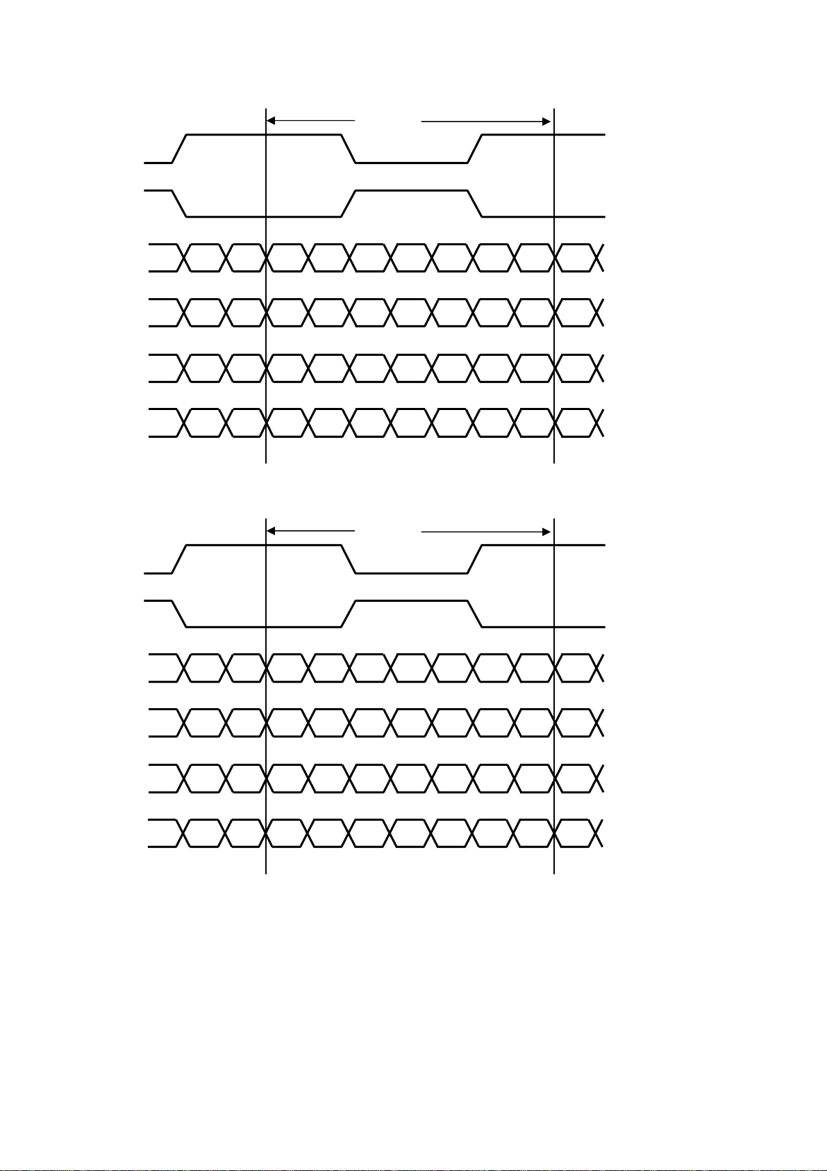
7.Timing characteristics of input signals
7-1.Timing characteristics
LD-22902A- 12
Remark
Clock
Parameter
Frequency
Symbol
1/Tc
Min.
50.0
Typ.
65
Max. Unit
80.0
MHz
1056 1344 1720 clock
Horizontal period
Horizontal period (High)
TH
THd
16.0
20.7
23.4
μs
1024 1024 1024 clock
ENAB
Vertical Frequency
Vertical period (High)
772
806
TV
13.3
TVd 768
768
16.7 18.0 ms
990
line
768 line
【*1】
【*1】 In case of using the long vertical period, the deterioration of display quality, flicker etc. may occur.
TH
THd
ENAB
DATA
1024 1024
(R,G,B)
12
Tc
768 767 768
ENAB
TV
7-2.Input Data Signals and Display Position on the screen
RGBR
( 1, 1 )
GB
( 2, 1 )
D(1,1) D(2,1) D(3,1) D( 1024 ,1)
12
TVd
D(1,2) D(2,2)
D(1,3)
R G B
D(1, 768 ) D( 1024 , 768 )
Page 17

8.Input Signals, Basic Display Colors and Gray Scale of Each Color
8-1.8 bit input
Data signal
Colors &
Gray scale
Gray
Scale
B0R4 B7B3 B4R5 R6 R7 G5 G6G0 G1 G2 G3
G7G4
B1 B2R0 R1 R2 R3
LD-22902A- 13
B5
B6
Black
Blue
Green
Cyan
Red
Basic Color
Magenta
Yellow
White
Black
↑
Darker
↑↑
↓↓
Brighter
Gray Scale of Red
↓
Red
- 000000000000000000000000
- 0000000000000000XX111111
- 00000000XX11111100000000
- 00000000XX111111XX111111
- XX1111110000000000000000
- XX11111100000000XX111111
- XX111111XX11111100000000
- XX111111XX111111XX111111
GS0 000000000000000000000000
GS1 100000000000000000000000
GS2 010000000000000000000000
↑↑↑
↓↓↓
GS250 100111110000000000000000
GS251 110111110000000000000000
GS252 X X 1111110000000000000000
Black
↑
Darker
↑↑
↓↓
Brighter
Gray Scale of Green
↓
Green
Black
↑
Darker
↑↑
↓↓
Brighter
Gray Scale of Blue
↓
Blue
GS0 000000000000000000000000
GS1 000000001000000000000000
GS2 000000000100000000000000
↑↑↑
↓↓↓
GS250 000000001001111100000000
GS251 000000001101111100000000
GS252 00000000XX11111100000000
GS0 000000000000000000000000
GS1 000000000000000010000000
GS2 000000000000000001000000
↑↑↑
↓↓
GS250 000000000000000010011111
GS251 000000000000000011011111
GS252 0000000000000000XX111111
↓
0 :Low level voltage 1 :High level voltage X :Don’t care
Each basic color can be displayed in253 gray scales from 8 bit data signals. According to the combination of、
total 24 bit data signals, the 16-million-color display can be achieved on the screen.
Page 18

8-2.6 bit input
LD-22902A- 14
Basic ColorGray Scale of RedGray Scale of GreenGray Scale of Blue
Colors &
Gray scale
Black
Blue
Green
Cyan
Red
Magenta
Yellow
White
Black
↑
Darker
↑
↓
Brighter
GrayScale
-
-
-
-
-
-
-
-
GS0
GS1
GS2
↓
↓
GS61
Data signal
R0 R1 R2 R3 R4 R5 G0 G1 G2 G3 G4 G5 B0 B1 B2 B3 B4 B5
000000000000000000
000000000000111111
000000111111000000
000000111111111111
111111000000000000
111111000000111111
111111111111000000
111111111111111111
000000000000000000
100000000000000000
010000000000000000
↓↓
↓
↓↓↓
101111000000000000
↓
Red
Black
↑
Darker
↑
↓
Brighter
↓
Green
Black
↑
Darker
↑
↓
Brighter
GS62
GS63
GS0
GS1
GS2
↓
↓
GS61
GS62
GS63
GS0
GS1
GS2
↓
↓
GS61
011111000000000000
111111000000000000
000000000000000000
000000100000000000
000000010000000000
↓↓
↓
↓↓↓
000000101111000000
000000011111000000
000000111111000000
000000000000000000
000000000000100000
000000000000010000
↓↓
↓
↓↓↓
000000000000101111
↓
Blue
GS62
GS63
000000000000011111
000000000000111111
Each basic color can be displayed in 64 gray scales from 6 bit data signals. According to the combination of
total 18 bit data signals, the 262,144-color display can be achieved on the screen.
Page 19

9.Optical Characteristics
LD-22902A-
Ta=+25℃, Vcc=+3.3V
15
Parameter
Viewing
Horizontal θ21,θ22
angle
range
Response Time
Vertical
White Black
Chromaticity of
White
Chromaticity of
Red
Chromaticity of
Green
Chromaticity of
Blue
Luminance of white
Symbol Min.
Condition Unit
70 80
θ11
θ12
CRContrast ratio
optimized
angle
45CR>10
70
450
τr +τd
Wx
Wy
0.255
0.275
Rx
Ry
Gx
θ=0°
Gy
Bx
By
Y
L1
280
Typ.
65
80
800
-
30
0.325
-
-
-
-
-
0.560
0.330
0.335
0.595
0.155
- 0.115
350
Max.
-
-
-
-
-
0.3550.305
0.375
-
-
-
-
-
-
-
Deg.
Deg.
Deg.
ms
cd/m
Remark
【*1,2,4】
【*2,4】
【*3,4】
【*4】
2
【*4】
White Uniformity
-- 1.33
【*5】
※The measurement shall be executed 30 minutes after lighting at rating.
The optical characteristics shall be measured in a dark room or equivalent state with the method shown
in Fig.2 below.
Photodetector
:Response time(BM-5A)
:Contrast/Luminance/Chromaticity(SR-3)
Photodetector:(EZ-CONTRAST)
Panel center(θ=0°)
TFT-LCD module
fig.2-1 Measuring method of Viewing angle range.
fig.2-2 Measuring method of contrast, luminance, response time,
and Chromaticity.
400mm
Field=1°
Panel center(θ=0°)
TFT-LCD module
Fig.2 Optical characteristics measurement method
Page 20

LD-22902A- 16
【*1】Definitions of viewing angle range:
θ22
Normal line
θ11
θ21
θ12
6 O'clock
【*2】Definition of contrast ratio:
Luminance with all pixels white
Contrast (CR)=The contrast ratio is defined as the following.
Luminance with all pixels black
【*3】Definition of response time:
The response time is defined as the following figure and shall be measured by switching the input signal for
"black" and "white".
White
100%
90%
(Relative Value)
Photodetector Output
10%
0%
τ
d
Black
White
τ
Time
【*4】This shall be measured at center of the screen. 256 512 768 pixel
【*5】Definition of white uniformity:
White uniformity is defined as the following with five measurements.
(①~⑤) 192
2
Maximum luminance of 5 points(①~⑤).
δw =
Maximum luminance of 5 points(①~⑤).
5
3
1
4
384
576
pixel
Page 21

LD-22902A- 17
10. Handling Precautions
a ) Be sure to turn off the power supply when inserting or disconnecting the cable.
b ) Since the front polarizer is easily damaged, pay attention not to scratch it.
c ) Wipe off water drop immediately. Long contact with water may cause discoloration or spots.
d ) When the panel surface is soiled, wipe it with absorbent cotton or other soft cloth.
e ) Since the panel is made of glass, it may break or crack if dropped or bumped on hard surface.
Handle with care.
f ) Since CMOS LSI is used in this module, take care of static electricity and injure the human earth
when handling. Observe all other precautionary requirements in handling components.
g ) Since there is a circuit board in the module back, stress is not added at the time of a design assembly.
Please make it like. If stress is added, there is a possibility that circuit parts may be damaged.
h ) It causes an irregular display and the defective indication, etc., when always put constant pressure
on the back of the module.
Please do not make the structure to press the back of the module.
i ) Do not expose the LCD panel to direct sunlight. Lightproof shade etc. should be attached
when LCD panel is used under such environment.
j ) Connect GND to stabilize against EMI and external noise.
k ) When handling LCD modules and assembling them into cabinets, please avoid that long-terms storage
in the environment of oxidization or deoxidization gas and the use of such materials as reagent, solvent,
adhesive, resin, etc. which generate these gasses, may cause corrosion and discoloration of the modules.
Do not use the LCD module under such environment.
l ) Liquid crystal contained in the panel may leak if the LCD is broken. Rinse it as soon as possible
if it gets inside your eye or mouth by mistake.
m ) Be careful when using it for long time with fixed pattern display as it may cause accidential image.
n ) Adjusting volume have been set optimally before shipment, so do not change any adjusted value.
If adjusted value is changed, the specification may not be satisfied.
o ) If a minute particle enters in the module and adheres to an optical material, it may cause display
non-uniformity issue, etc. Therefore, fine-pitch filters have to be installed to cooling and inhalation
hole if you intend to install a fan.
p) The polarizer surface on the panel is treated with Anti-Glare for low reflection. In case of attaching
protective board over the LCD, be careful about the optical interface fringe etc. which degrades display
quality.
q ) Notice : Never take to pieces the module , because it will cause failure.
Please do not peel off the Black tape pasted to the product.
An abnormal display by changing in quality of the polarizing plate might occur regardless of contact
r)
or no contact to the polarizing plate, because of epoxy resin (amine system curing agent)
that comes out from the material and the packaging material used for the set side, the silicon adhesive
(dealcoholization system and oxime system), and the tray blowing agents (azo-compound), etc.
Please confirm adaptability with your employed material.
Page 22

11.Packing form
t
a) Piling number of cartons : MAX.6
b) Package quantity in one carton: 10pcs
c) Carton size(TYP): 450mm(W) × 312mm(D)×400mm(H)
LD-22902A- 18
d)
Total mass of one carton filled with full modules(10pcs): 9.8kg
12.Reliability test items
No.
1
2
3
4
5
6
7
8
Test item
High temperature
storage test
Low temperature
strage test
High temperature
& high humidity
operation test
High temperature
operation test
Low temperature
operation test
Vibration test 【Note1】
Shock test 【Note1】
Thermal shock tes
Ambient temperature 70℃ 240H
Ambient temperature -30℃ 240H
Ambient temperature 40℃、Humidity 95% RH 240H
(No condensation.)
Panel surface 70℃ 240H
Ambient temperature 0℃ 240H
<Sin wave>
Frequency :10~57Hz/Vibration width (one side) :0.076mm
:57~500Hz/Gravity:9.8m/s2
Sweep time:11minutes
Test period :3H(X,Y,Z direction 1H)
Max. gravity:490m/s2 Pulse width:11ms
Direction:±X,±Y,±Z Test period :1time/1direction
-30℃[0.5h]~70℃[0.5h]/50cycles
Conditions
Remark
【Note1】
【Note1】
【Note1】
【Note1】
【Note1】
【Note1】
【Note1】 Under the display quality test conditions with normal operation state, these shall be no change
which may affect practical display function. (normal operation state:Temperature:15~35℃,
Humidity:45~75%, Atmospheric pressure:86~106kpa)
Page 23

13.Others
13-1.Lot No Label:
A)Module serial label
The label that displays SHARP・Model No.( LQ150X1LG93)・Lot No. is stuck on the back of the module.
LD-22902A- 19
SHARP
LQ150X1LG93
XXXXXXXXXX
B)Backlight serial label
The label that displays the model No. and lot No. for the backlight is stuck on the back of the module.
******-*
******-**
13-2.Packing box Label:
The label that displays ①Model number( LQ150X1LG93) ②Lot number ③Quantity of module is stuck
on the packing box. Moreover, the display of bar code also applies to this.
社内品番:
Barcode(①)
Model No.
Bar Code(Lot No.)
Lot No.
Model No.
(Figure and alphabet)
Lot No.
(Figure and alphabet)
(4S) LQ150X1LG93
Lot No display method
Production year
(Last digit of dominical year)
Production month (1-9X, Y, Z)
(Figure and alphabet)
Serial No.
Assembly site code
Discernment code
Lot No. : (1T) 2009. 06. 01 **
Barcode(②)
Quantity : (Q) 10 pcs
Barcode(③)
ユーザー品番 :
シャープ物流用ラベルです。
Our management product number might be filled
(Example: LQ150X1LG93A etc.)
① Model number( LQ150X1LG93)
② Lot number (DATA)
③ Quantity of module
A right picture is written to the packing box of module for the RoHS restriction.
R.C.(RoHs Compliance)means these parts have corresponded with the RoHs directive.
※
This module corresponds from the first sample to RoHS Directive.
13-3.
The ozone-depleting substances is not used.
13-4. If any problem occurs in relation to the description of this specification , it shall be resolved
through discussion with spirit of cooperation.
R.C.
Page 24

14.Storage conditions
Environmental condition range of storage temperature and humidity
Temperature 0 to 40 degrees Celsius
Relative humidity 95% and below
【Note】Please refer below as a mean value of the environmental conditions.
Summer time temperature 20 to 35 degrees Celsius humidity , 85% and below
Winter time temperature 5 to 15 degrees Celsius humidity , 85% and below
Please maintain within 240 hours of accumulated length of storage time, with conditions of 40 degrees
Celsius and room humidity of 95%.
Direct sun light
Please keep the product in a dark room or cover the product to protect from direct sun light.
Atmospheric condition
Please refrain from keeping the product with possible corrosive gas or volatile flux.
Prevention of dew
Please store the product carton either on a wooden pallet or a stand / rack to prevent dew.
Do not place directly on the floor. In addition, to obtain moderate ventilation in between the pallet’s
top and bottom surfaces, pile the cartons up in a single direction and in order.
Please place the product cartons away from the storage wall.
Storage period
Within above mentioned conditions, maximum storage period should be one year.
LD-22902A- 20
Page 25

LD-22902A- 21
Fig. 1 : LQ150X1LG93 OUTLINE DIMENSIONS
Page 26

LD-22902A- 22
Fig.3 : PACKING FORM
Page 27

Technical Document
LCD Specification
LCD Group
NORTH AMERICA
Sharp Microelectronics of the Americas
5700 NW Pacific Rim Blvd.
Camas, WA 98607, U.S.A.
Phone: (1) 360-834-8700
Fax: (1) 360-834-8903
www.sharpsma.com
TAIWAN
Sharp Electronic Components
(Taiwan) Corporation
8F-A, No. 16, Sec. 4, Nanking E. Rd.
Taipei, Taiwan, Republic of China
Phone: (886) 2-2577-7341
Fax: (886) 2-2577-7326/2-2577-7328
CHINA
Sharp Microelectronics of China
(Shanghai) Co., Ltd.
28 Xin Jin Qiao Road King Tower 16F
Pudong Shanghai, 201206 P.R. China
Phone: (86) 21-5854-7710/21-5834-6056
Fax: (86) 21-5854-4340/21-5834-6057
Head Office:
No. 360, Bashen Road,
Xin Development Bldg. 22
Waigaoqiao Free Trade Zone Shanghai
200131 P.R. China
Email: smc@china.global.sharp.co.jp
EUROPE
Sharp Microelectronics Europe
Division of Sharp Electronics (Europe) GmbH
Sonninstrasse 3
20097 Hamburg, Germany
Phone: 49 (0)180 507 35 07
Fax: (49) 40-2376-2232
www.sharpsme.com
SINGAPORE
Sharp Electronics (Singapore) PTE., Ltd.
438A, Alexandra Road, #05-01/02
Alexandra Technopark,
Singapore 119967
Phone: (65) 271-3566
Fax: (65) 271-3855
KOREA
Sharp Electronic Components
(Korea) Corporation
RM 501 Geosung B/D, 541
Dohwa-dong, Mapo-ku
Seoul 121-701, Korea
Phone: (82) 2-711-5813 ~ 8
Fax: (82) 2-711-5819
JAPAN
Sharp Corporation
Electronic Components & Devices
22-22 Nagaike-cho, Abeno-Ku
Osaka 545-8522, Japan
Phone: (81) 6-6621-1221
Fax: (81) 6117-725300/6117-725301
www.sharp-world.com
HONG KONG
Sharp-Roxy (Hong Kong) Ltd.
Level 26, Tower 1, Kowloon Commerce Centre,
No. 51, Kwai Cheong Road, Kwai Chung,
New Territories, Hong Kong
Phone: (852) 28229311
Fax: (852) 28660779
www.sharp.com.hk
Shenzhen Representative Office:
Room 602-603, 6/F.,
International Chamber of Commerce Tower,
168 Fuhua Rd. 3, CBD,
Futian District, Shenzhen 518048,
Guangdong, P.R. China
Phone: (86) 755-88313505
Fax: (86) 755-88313515
SPECIFICATIONS ARE SUBJECT TO CHANGE WITHOUT NOTICE.
Suggested applications (if any) are for standard use; See Important Restrictions for
limitations on special applications. See Limited Warranty for SHARP’s product warranty.
The Limited Warranty is in lieu, and exclusive of, all other warranties, express or implied.
ALL EXPRESS AN D IMPLIED WARRANTIES, INCLUDI NG THE WARRANTI ES OF
MERCHANTABILITY, FITNESS FOR USE AND FITNESS FOR A PARTICULAR PU RPOSE,
ARE SPECI FICALLY EXCLUDED. In no event will SHARP be liable, or responsible in
any way, for any incidental or consequential economic or property damage.
 Loading...