

Page 1

Technical Document
LCD Specification
LCD Group
LQ150X1LG76 LCD Module
Product Specification
Ju ly 2011
XGA Normally Black module with contrast of
700:1 and brightness of 450 nits.
Anti-reflective,anti-glare,and hard coated.
Page 2
CONTENTS
No. Item Page
-- COVER 1
-- CONTENTS 2
1 APPLICATION 3
2 OVERVIEW 4
3 ABSOLUTE MAXIMUM RATINGS 5
4 ELECTRICAL CHARACTERISTICS 5, 6, 7
5 INTERFACE PIN CONNECTION 8, 9
6 INTERFACE TIMING 10, 11, 12, 13, 14
7 BLOCK DIAGRAM 15
8 MECHANICAL SPECIFICATION 16, 17
9 OPTICAL CHARACTERISTICS 18, 19, 20
10 RELIABILITY TEST CONDITION 21
11 OTHER FEATURE 22
12 HANDLING PRECAUTIONS FOR TFT-LCD MODULE 23, 24, 25
(2/25)
Page 3

1. APPLICATION
This specification applies to color TFT-LCD module,
(1) Standard Usage
Computers, office equipment, factory automation equipment, test and measurement
equipment, communications, transportation equipment(automobiles, ships, trains, etc.),
provided, however, that operation is not influenced by TFT-LCD directly.
(2) Special Usage
Medical equipment, safety equipment, transportation equipment, provided, however, that
TFT-LCD is necessary to its operation.
(3) Specific Usage
Cockpit Equipment, military systems, aerospace equipment, nuclear reactor control
systems, life support systems and any other equipment.
LQ150X1LG76.
(3/25)
Page 4
2. OVERVIEW
is 15.0” color TFT-LCD (Thin Film Transistor Liquid Crystal Display) module
LQ150X1LG76
composed of LCD panel, driver ICs, control circuit, LED driver and backlight unit.
By applying 6 bit or 8 bit digital data, 1024 × 768, 262k-color or 16.7M-color images are displayed
on the 15.0” diagonal screen. Input power voltages are 3.3 V for LCD driving and 12.0 V for
backlight unit.
The type of data and control signals are digital and transmitted via LVDS interface per Typ. 65
MHz clock cycle.
General specifications are summarized in the following table:
ITEM SPECIFICATION
Display Area (mm)
Number of Dots
304.1(H) × 228.1(V)
(15.0-inch diagonal)
1024 × 3 (H) × 768 (V)
Pixel Pitch (mm)
Color Pixel Arrangement RGB vertical stripe
Display Mode Normally white
Number of Color 262k(6 bit/color), 16.7M(8 bit/color)
Luminance (cd/m2) 450
Viewing Angle (CR ≥ 10) −80∼80°(H), −70∼70°(V)
Surface Treatment Anti-glare and hard-coating 3H
Electrical Interface LVDS (6 bit/8 bit)
Viewing direction
Module Size (mm)
Module Mass (g) 1050
Backlight Unit LED, Edge-light, Unreplaceable
Characteristic value without any note is typical value.
Less gray scale reversal: 12 o'clock
0.297 (H) × 0.297 (V)
Higher Contrast ratio: 6 o'clock
326.5 (W) × 253.5 (H) × 12.0(D)
(4/25)
Page 5

3. ABSOLUTE MAXIMUM RATINGS
ITEM SYMBOL MIN. MAX. UNIT
Power Supply Voltage for LCD VCC 0 4.0 V
Logic Input Voltage VI
Backlight Power Supply Input Voltage VL
Backlight ON-OFF BLEN
Light Dimming Control (PWM) input voltage V
Operation Temperature (Panel)
Operation Temperature (Ambient)
Storage Temperature
Note 1,2)
T
Note 2)
T
Note 2)
T
PDIM
op(Panel)
op(Ambient)
stg
−0.3
−0.3
−0.3
−0.3
0 65 °C
0 65 °C
−20
VCC+0.3 V
14.0 V
VL V
5.8 V
65 °C
[Note]
1) The relative temperature and humidity range are 90%RHMax. (Ta ≤ 40°C).
2) The maximum wet bulb temperature ≤ 39°C (Ta > 40°C) and without dewing.
3) If you use the product in a environment which over the definition of temperature and humidity
too long to effect the result of eye-aching.
4) If you operate the product in normal temperature range, the center surface of panel should be
under 65°C.
4. ELECTRICAL CHARACTERISTICS
(1) TFT-LCD
Ambient temperature: Ta = 25°C
ITEM SYMBOL MIN. TYP. MAX. UNIT Remarks
Power Supply Voltages for LCD VCC 3.0 3.3 3.6 V *1)
Power Supply Currents for LCD ICC -- 480 800 mA *2)
Permissive Input Ripple Voltage VRP -- -- 100 mVp-p VCC = +3.3V
High VIH
0.8×VCC
-- VCC V MODE
Logic Input Voltage
Low VIL 0 --
0.2×VCC
V MODE
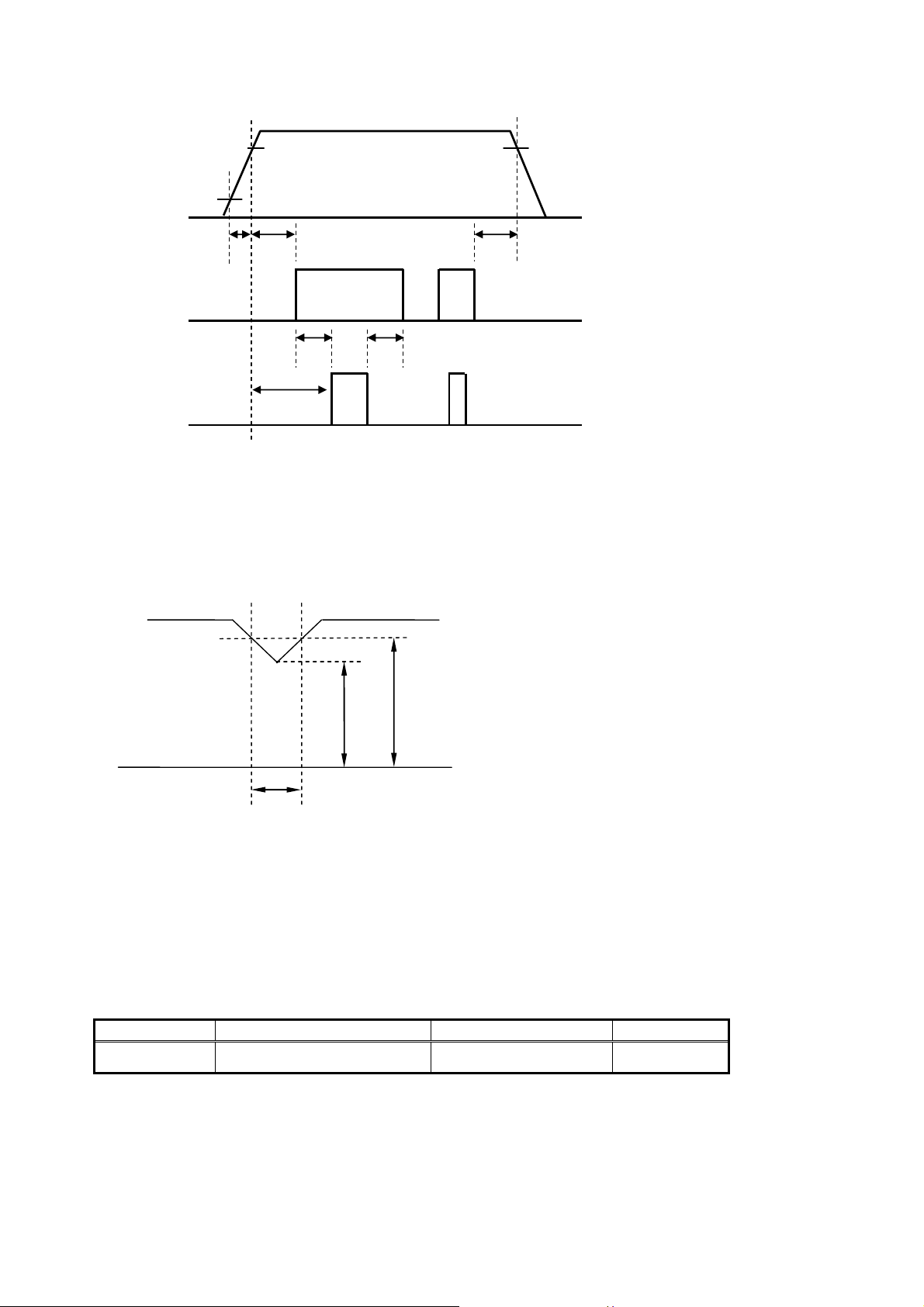
*1) Power and signals sequence:
0.5 ≤ t1 ≤ 10 ms 200 ms ≤ t4
0 < t2 ≤ 50 ms 200 ms ≤ t5
t6
t1
≤
VCC
0.9VCC
data
0.1VCC
t2
t3
t4
0.1VCC
0 < t3 ≤ 50 ms 0 ms
0.9VCC
LCD Power Supply
Logic Signal
Backlight Power Supply
0.1VCC
t5 t6
data: RGB DATA, DCLK, DENA, MODE
(5/25)
Page 6
VCC-dip conditions:
1) When 2.7 V
≤
VCC < 3.0 V, td ≤ 10 ms
2) When VCC < 2.7 V
VCC-dip conditions should also follow the power and signals sequence.
3.0 V
2.7 V
VCC
td
*2) VCC = +3.3 V , f
=48.36 kHz, fV=60 Hz, f
H
=65 MHz
CLK
Display image at typical power supply current value is 256-gray-bar pattern (8 bit), 768 line
mode.
*3) Fuse
Parameter Fuse Type Name Supplier Remark
VCC F0603FA3000V032T AEM *)
*) The power supply capacity should be designed to be more than the fusing current.
(2) Backlight Ta=25°C
ITEM SYMBOL MIN. TYP. MAX. UNIT Remarks
Power Supply Input Voltage VL 10.8 12.0 13.2 V *1)
Power Supply Input Current IL 600 700 850 mA *2, *4)
Power Supply Input Current PL -- 8.4 9.2 W
Dimming=100%,
VL=12.0V
High 2.5 -- VL V ON
Backlight ON-OFF
Low
Light Dimming Control
(PWM) input voltage
High 1.8 -- 5.0 V ON
Low
PWM frequency f
Pulse width of PDIM t
BLEN
0 -- 0.4 V OFF
PDIM
V
0 -- 0.8 V OFF
100 400 500 Hz *3)
PDIM
100 -- DC us *3)
PDIM
LED Life Time LT 80,000 100,000 -- h *5), *6)
(6/25)
Page 7
*1) Power and signals sequence:
90% 90%
VL
10%
t1 t2 t6
PDIM
BLEN
t4
12V(Typ)
20 ≤ t1 [ms] 100 ≤ t4 [ms]
0 ≤ t2 [ms] 0 ≤ t5 [ms]
0 ≤ t3 [ms] 1 ≤ t6 [ms]
VL-dip conditions:
1) When 9.72 V
VL < 10.8 V, td ≤ 10 ms
≤
2) When VL < 9.72V
VL-dip conditions should also follow the power and signals sequence.
t5t3
VL
10.8 V
9.72 V
td
*2) Includes rush current. PL≠VL×IL
*3) Lower frequency causes the flicker or the image breaking of motion picture.
Depending on the PDIM signal integrity (jitter etc.), the flicker may be visible. Please evaluate in
advance.
The dimming ratio (D) can be calculated by following equation:
D = f
PDIM
× t
. Therefore, the minimum dimming ratio is f
PDIM
PDIM
× t
PDIM(min)
*4) Fuse
Parameter Fuse Type Name Supplier Remark
VL F0603HI2000V032T AEM *)
*) The power supply capacity should be designed to be more than the fusing current.
*5) LED life time is defined as the time when the brightness becomes 50% of the initial value.
*6) The life time of the backlight depends on the ambient temperature. The life time will decrease
under high temperature.
(7/25)
Page 8
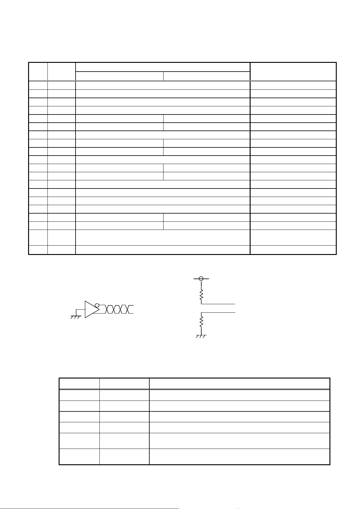
5. INTERFACE PIN CONNECTION
V
(1) CN 1(Interface Signal)
Used connector: MSB240420(STM)
Corresponding connector: DF14-20S-1.25C(Hirose)
Pin
No.
Symbol
1 VCC
2 VCC
3 GND
4 GND
5
Link 0−
Function (ISP 6 bit compatibility mode)
6 bit input 8 bit input
+3.3 V Power supply
+3.3 V Power supply
GND
GND
R0, R1, R2, R3, R4, R5, G0 R2, R3, R4, R5, R6, R7, G2
Function (ISP 8 bit
compatibility mode)
←
←
←
←
R0, R1, R2, R3, R4, R5, G0
6 Link 0+ R0, R1, R2, R3, R4, R5, G0 R2, R3, R4, R5, R6, R7, G2 R0, R1, R2, R3, R4, R5, G0
7 GND
8
Link 1−
G1, G2, G3, G4, G5, B0, B1 G3, G4, G5, G6, G7, B2, B3
GND
←
G1, G2, G3, G4, G5, B0, B1
9 Link 1+ G1, G2, G3, G4, G5, B0, B1 G3, G4, G5, G6, G7, B2, B3 G1, G2, G3, G4, G5, B0, B1
10 GND
11
Link 2−
B2, B3, B4, B5, DENA B4, B5, B6, B7, DENA
GND
←
B2, B3, B4, B5, DENA
12 Link 2+ B2, B3, B4, B5, DENA B4, B5, B6, B7, DENA B2, B3, B4, B5, DENA
13 GND
14
CLKIN− Clock − ←
15 CLKIN+
16 GND
17
Link3−
See: *2) R0, R1, G0, G1, B0, B1
GND
Clock +
GND
←
←
←
R6, R7, G6, G7, B6, B7
18 Link3+ See: *2) R0, R1, G0, G1, B0, B1 R6, R7, G6, G7, B6, B7
19 MODE Low=ISP 6 bit compatibility mode
20 GND
GND
High=ISP
8 bit compatibility mode
←
*1) Metal frame is connected to signal GND.
*2) Recommended wiring of Pin 17,18 (6 bit input)
LVDS
transmitter
(2) CN 2(Backlight)
Backlight-side connector: CR03-P06H2B-2 (CONNTEK)
Corresponding connector: CR03-S06C3 (CONNTEK), FI-S6S (JAE)
Pin No.: The left side pin is No.1.
Pin No. Symbol Function
1 VL Power Supply Input Voltage
2 VL Power Supply Input Voltage
3 GND GND
4 GND GND
5 BLEN
6 V
*1) BLEN is NOT designed for dimming.
LOW data
PDIM
Pin 17
Pin 18
CC
680
Ω
Pin 17
or
620
Ω
Pin 18
Backlight ON-OFF
(High: ON, Low: OFF)
Light Dimming Control (PWM) Input Voltage
(High active)
(8/25)
Page 9

(3) ISP data mapping
a. ISP 6 bit compatibility mode(6 bit input)
CLKIN+/-
Link0+/-
Link1+/-
Link2+/-
b. ISP 6 bit compatibility mode(8 bit input)
CLKIN+/-
Link0+/-
Link1+/-
1CLK
G0 R5 R4 R3 R2 R0
B1 B0 G5 G4 G3 G1
DENA
B5 B4 B2
G2 R7 R6 R5 R4 R2
B3 B2 G7 G6 G5 G3
R1
G2
B3
1CLK
R3
G4
Link2+/-
Link3+/-
c. ISP 8 bit compatibility mode
CLKIN+/-
Link0+/-
Link1+/-
Link2+/-
Link3+/-
DENA
B7 B6 B4
B1 B0 G1 G0 R0
B5
R1
1CLK
G0
B1
DENA
R5
B0
B7
R4
G5
B6
R3
G4
B5
G7
R2
G3
B4
G6
R1
G2
B3
R7
R0
G1
B2
R6
(9/25)
Page 10

6. INTERFACE TIMING
LVDS transmitter input signal
(1) Timing Specifications
ITEM SYMBOL MIN TYP MAX UNIT
DCLK
Frequency f
Period t
Active Time t
Blanking Time t
CLK
CLK
HA
HB
50 65 80 MHz
12.5 15.4 20 ns
1024 1024 1024 t
20 320 -- t
Horizontal
DENA
Frequency f
Period t
Active Time t
Blanking Time t
H
H
VA
VB
42.4 48.4 60 kHz
16.6 20.7 23.6
768 768 768 t
3 38 -- t
Vertical
Frequency f
Period t
V
V
55 60 75 Hz
13.3 16.7 18.2 ms
[Note]
1) DENA (Data Enable) should always be positive polarity as shown in the timing specification.
2) DCLK should appear during all invalid period.
3) LVDS timing follows the timing specifications of LVDS receiver IC: THC63LVDF84B(Thine).
4) In case of blanking time fluctuation, please satisfy following condition.
t
VBn
> t
VBn-1
− 3(tH)
CLK
CLK
μs
H
H
(10/25)
Page 11

(2) Timing Chart
V
V
a. Horizontal Timing Chart
DCLK
DATA
(R, G , B)
DENA
tHB
t
CLK
First Data Last Data
1 2
3Invalid Data Invalid Data
tHA
1023 1024
b. Vertical Timing Chart
LINE DATA
DENA
tVB
t
H
t
1 2 767 768 3In valid Dat a In valid Dat a
t
A
(11/25)
Page 12

(3) Color Data Assignment
a. 6 bit input
COLOR
INPUT DATA
R DATA G DATA B DATA
R5 R4 R3 R2 R1 R0 G5 G4 G3 G2 G1 G0 B5 B4 B3 B2 B1 B0
MSB LSB MSB LSB MSB LSB
BLACK 0 0 0 0 0 0 0 0 0 0 0 0 0 0 0 0 0 0
RED(63) 1 1 1 1 1 1 0 0 0 0 0 0 0 0 0 0 0 0
GREEN(63) 0 0 0 0 0 0 1 1 1 1 1 1 0 0 0 0 0 0
BASIC BLUE(63) 0 0 0 0 0 0 0 0 0 0 0 0 1 1 1 1 1 1
COLOR CYAN 0 0 0 0 0 0 1 1 1 1 1 1 1 1 1 1 1 1
MAGENTA 1 1 1 1 1 1 0 0 0 0 0 0 1 1 1 1 1 1
YELLOW 1 1 1 1 1 1 1 1 1 1 1 1 0 0 0 0 0 0
WHITE 1 1 1 1 1 1 1 1 1 1 1 1 1 1 1 1 1 1
RED(1) 0 0 0 0 0 1 0 0 0 0 0 0 0 0 0 0 0 0
RED(2) 0 0 0 0 1 0 0 0 0 0 0 0 0 0 0 0 0 0
RED
RED(62) 1 1 1 1 1 0 0 0 0 0 0 0 0 0 0 0 0 0
RED(63) 1 1 1 1 1 1 0 0 0 0 0 0 0 0 0 0 0 0
GREEN(1) 0 0 0 0 0 0 0 0 0 0 0 1 0 0 0 0 0 0
GREEN(2) 0 0 0 0 0 0 0 0 0 0 1 0 0 0 0 0 0 0
GREEN
GREEN(62) 0 0 0 0 0 0 1 1 1 1 1 0 0 0 0 0 0 0
GREEN(63) 0 0 0 0 0 0 1 1 1 1 1 1 0 0 0 0 0 0
BLUE(1) 0 0 0 0 0 0 0 0 0 0 0 0 0 0 0 0 0 1
BLUE(2) 0 0 0 0 0 0 0 0 0 0 0 0 0 0 0 0 1 0
BLUE
BLUE(62) 0 0 0 0 0 0 0 0 0 0 0 0 1 1 1 1 1 0
BLUE(63) 0 0 0 0 0 0 0 0 0 0 0 0 1 1 1 1 1 1
[Note]
1) Definition of gray scale
Color (n) --- n indicates gray scale level.
Higher n means brighter level.
2) Data
1:High, 0: Low
(12/25)
Page 13

b. 8 bit input
INPUT DATA
BASIC
COLOR
RED
GREEN
COLOR
BLACK
RED(255)
GREEN(255)
BLUE(255)
CYAN
MAGENTA
YELLOW
WHITE
RED(1)
RED(2)
RED(255)
GREEN(1)
GREEN(2)
GREEN(255)
R DATA G DATA B DATA
R7 R6 R5 R4 R3 R2 R1 R0 G7 G6 G5 G4 G3 G2 G1 G0 B7 B6 B5 B4 B3 B2 B1 B0
MSB LSB MSB LSB MSB LSB
0 0 0 0 0 0 0 0 0 0 0 0 0 0 0 0 0 0 0 0 0 0 0 0
1 1 1 1 1 1 1 1 0 0 0 0 0 0 0 0 0 0 0 0 0 0 0 0
0 0 0 0 0 0 0 0 1 1 1 1 1 1 1 1 0 0 0 0 0 0 0 0
0 0 0 0 0 0 0 0 0 0 0 0 0 0 0 0 1 1 1 1 1 1 1 1
0 0 0 0 0 0 0 0 1 1 1 1 1 1 1 1 1 1 1 1 1 1 1 1
1 1 1 1 1 1 1 1 0 0 0 0 0 0 0 0 1 1 1 1 1 1 1 1
1 1 1 1 1 1 1 1 1 1 1 1 1 1 1 1 0 0 0 0 0 0 0 0
1 1 1 1 1 1 1 1 1 1 1 1 1 1 1 1 1 1 1 1 1 1 1 1
0 0 0 0 0 0 0 1 0 0 0 0 0 0 0 0 0 0 0 0 0 0 0 0
0 0 0 0 0 0 1 0 0 0 0 0 0 0 0 0 0 0 0 0 0 0 0 0
1 1 1 1 1 1
1
1
0 0 0 0 0 0 0 0 0 0 0 0 0 0 0 0
0 0 0 0 0 0 0 0 0 0 0 0 0 0 0 1 0 0 0 0 0 0 0 0
0 0 0 0 0 0 0 0 0 0 0 0 0 0 1 0 0 0 0 0 0 0 0 0
0 0 0 0 0 0 0 0 1 1 1 1 1 1 1 1 0 0 0 0 0 0 0 0
BLUE(1)
BLUE(2)
BLUE
BLUE(255)
[Note]
1) Definition of gray scale
Color (n) --- n indicates gray scale level.
2) Data
1:High, 0: Low
0 0 0 0 0 0 0 0 0 0 0 0 0 0 0 0 0 0 0 0 0 0 0 1
0 0 0 0 0 0 0 0 0 0 0 0 0 0 0 0 0 0 0 0 0 0 1 0
0 0 0 0 0 0 0 0 0 0 0 0 0 0 0 0 1 1 1 1 1 1 1 1
Higher n means brighter level.
(13/25)
Page 14

(4) Display Position and Scan Direction
D(X,Y) shows the data number of input signal.
D(1,1) D(1024,1)
D(1,768)
D(1024,768)
(14/25)
Page 15

7. BLOCK DIAGRAM
CN1
Timing signal
Display data
Timing
Controller
G1
G2
TFT-LCD
Power
Brightness/
ON/OFF
Control
Power
I/F Connector
CN2
I/F Connector
Power
Supply
Circuit
Power
Supply
Circuit
Driver(gate)
G768
S1
S2
S3071
Driver(source)
LED B/L
S3072
(15/25)
Page 16

8. MECHANICAL SPECIFICATIONS
(1) Front Side
(Unit: mm)
(16/25)
Page 17

(2) Rear Side
(Unit: mm)
(17/25)
Page 18

9. OPTICAL CHARACTERISTICS
Ta=25°C, VCC=3.3V, VL=12.0V, Input Signals: Typ. values shown in Section 6
ITEM SYMBOL CONDITION MIN TYP MAX UNIT Remarks
Contrast Ratio CR
Luminance Lw
Luminance Uniformity
ΔLw θ
tr
Response Time
tf
Viewing
Angle
Horizontal
Vertical
θ
H
θ
V
θ
=0°, θH=0°
V
θ
=0°, θH=0°
V
=0°, θH=0°
V
θ
=0°, θH=0°
V
θ
=0°, θH=0°
V
−65~65 −80~80
CR ≥ 10
450 700 -- -- *1)*2)*4)
2
360 450 -- cd/m
*1)*4)
75 -- -- % *1)*3)*4)
-- 2 -- ms *1)*4)*5)
-- 10 -- ms *1)*4)*5)
-- ° *1)*4)
−55~55 −70~70
-- ° *1)*4)
Image sticking tis 2 h -- -- 2 s --
Red
Color Gx 0.295 0.345 0.395
Green
Coordinates
Blue
White
Rx 0.584 0.634 0.684
Ry 0.295 0.345 0.395
Gy
θ
=0°, θH=0°
V
0.545 0.595 0.645 --
*1)*4)
Bx 0.100 0.150 0.200
By 0.023 0.073 0.123
Wx 0.263 0.313 0.363
Wy 0.279 0.329 0.379
[Note]
These items are measured using SR-UL1R(TOPCON) for color coordinates, and BM-5A (TOPCON)
for others under the dark room condition. (no ambient light) after more than 20 minutes from
turning on the backlight unless noted.
Condition: V
= 1.8V ∼ 5.0V DC
PDIM
Measurement method for luminance and color coordinates is as follows.
(18/25)
Page 19

*1) Measurement Point
Contrast Ratio, Luminance, Response Time, Viewing Angle, Color Coordinates: Display Center
Luminance Uniformity: point 1∼9 shown in a figure below
384
512
*2) Definition of Contrast Ratio
CR=Luminance with all white pixels / Luminance with all black pixels
*3) Definition of Luminance Uniformity
ΔLw=[Lw(Min)/Lw(Max)]×100%
*4) Definition of Viewing Angle (θ
, θH)
V
θ
V
θ
H
Upper
(1024,768)
Left
Lower
Right
(19/25)
Page 20

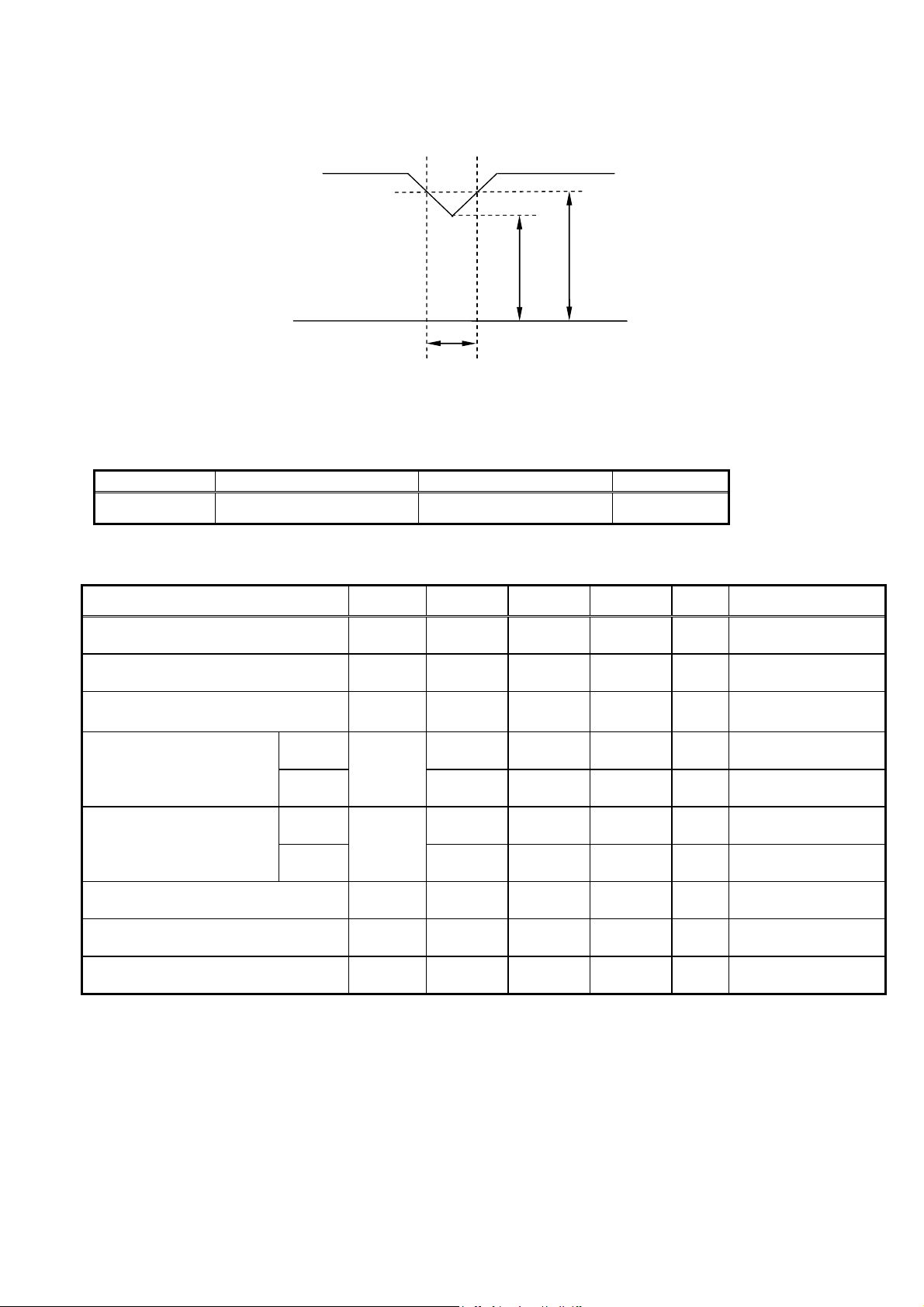
*5) Definition of Response Time
White
Luminance
tr
90 %
10 %
Black
90 %
10 %
tf
(20/25)
Page 21

10. RELIABILITY TEST CONDITION
(1) Temperature and Humidity
TEST ITEM CONDITIONS
HIGH TEMPERATURE
HIGH HUMIDITY OPERATION
HIGH TEMPERATURE OPERATION 65°C, 240 h
LOW TEMPERATURE OPERATION 0°C, 240 h
HIGH TEMPERATURE STORAGE 65°C, 240 h
LOW TEMPERATURE STORAGE
THERMAL SHOCK (NON-OPERATION)
(2) Shock & Vibration
ITEM CONDITIONS
Shock level: 1470 m/s
SHOCK
(NON-OPERATION)
Waveform: half sinusoidal wave, 2 ms
Number of shocks: one shock input in each direction of three mutually
perpendicular axes for a total of six shock inputs
2
(150G)
40°C, 90%RH, 240h
(No condensation)
−20°C, 240 h
−20°C (0.5 h) ∼ 65°C (0.5 h),
100 cycles
Vibration level: 9.8 m/s2 (1.0G)
Waveform: sinusoidal
VIBRATION
(NON-OPERATION)
(3) ESD Test
ITEM CONDITIONS
CONTACT DISCHARGE
(OPERATION)
SIGNAL PIN DISCHARGE
(NON-OPERATION)
Frequency range: 5 to 500 Hz
Frequency sweep rate: 0.5 octave /min
Duration: one sweep from 5 to 500 Hz in each of three mutually
perpendicular axis(each x,y,z axis: 1 hour, total 3 hours)
150pF, 330Ω, ±8kV, 10 times at 1 sec interval
200pF, 0Ω, ±200V, 10 times at 1 sec interval
(4) Judgment standard
The judgment of the above tests should be made as follow:
Pass: Normal display image, no damage of the display function. (ex. no line defect)
Partial transformation of the module parts should be ignored.
Fail: No display image, damage of the display function. (ex. line defect)
(21/25)
Page 22

11. OTHER FEATURE
This LCD module complies with RoHS*) directive.
*)
RoHS: Restriction of the use of certain hazardous substances in electrical and electronic
equipment
(22/25)
Page 23

12. HANDLING PRECAUTIONS FOR TFT-LCD MODULE
Please pay attention to the followings in handling TFT-LCD products;
(1) ASSEMBLY PRECAUTION
a. Please mount the LCD module by using mounting hole with a screw clamping torque less than
0.36 Nm. Please do not bend or wrench the LCD module in assembling. Please do not drop,
bend or twist the LCD module in handling.
b. Please design display housing in accordance with the following guide lines.
(a) Housing case must be designed carefully so as not to put stresses on LCD and not to
wrench module.
(b) Under high temperature environment, performance and life time of LED may heavily
shorten. When you design with our LCD product, please consider radiating heat and
ventilation for good heat management.
(c) Keep sufficient clearance between LCD module back surface and housing when the LCD
module is mounted. Approximately 1.0mm of the clearance in the design is recommended
taking into account the tolerance of LCD module thickness and mounting structure height
on the housing.
(d) When some parts, such as, FPC cable and ferrite plate, are installed underneath the LCD
module, still sufficient clearance is required, such as 0.5mm. This clearance is, especially, to
be reconsidered when the additional parts are implemented for EMI countermeasure.
(e) Keep sufficient clearance between LCD module and the others parts, such as inverter and
speaker so as not to interfere the LCD module. Approximately 1.0 mm of the clearance in
the design is recommended.
(f) To avoid local elevation/decrease of temperature, considering location of heating element,
heat release, thermal design should be done.
c. Please do not push or scratch LCD panel surface with anything hard. And do not soil LCD
panel surface by touching with bare hands. (Polarizer film, surface of LCD panel is easy to be
flawed.)
d. Please wipe off LCD panel surface with absorbent cotton or soft cloth in case of it being soiled.
e. Please wipe off drops of adhesives like saliva and water on LCD panel surface immediately.
They might damage to cause panel surface variation and color change.
f. Please do not take a LCD module to pieces and reconstruct it. Resolving and reconstructing
modules may cause them not to work well.
g. Please do not touch metal frames with bare hands and soiled gloves. A color change of the metal
frames can happen during a long preservation of soiled LCD modules.
h. Please handle metal frame carefully because edge of metal frame is very sharp.
(23/25)
Page 24

i. Please connect the metal frame of LCD module to GND in order to minimize the effect of
external noise and EMI.
j. Be sure to connect the cables and the connecters correctly.
(2) OPERATING PRECAUTIONS
a. Please be sure to turn off the power supply before connecting and disconnecting signal input
cable.
b. Please do not change variable resistance settings in LCD module. They are adjusted to the
most suitable value. If they are changed, it might happen LCD does not satisfy the
characteristics specification.
c. The interface signal speed is very high. Please pay attention to transmission line design and
other high speed signal precautions to satisfy signal specification.
d. Condensation might happen on the surface and inside of LCD module in case of sudden change
of ambient temperature. Please take care so as not to cause any damage mentioned on (1)-d.
e. Please pay attention not to display the same pattern for very long time. Image sticking might
happen on LCD. Although image sticking may disappear as the operation time proceeds,
screen saver function is recommended not to cause image sticking.
f. Please obey the same safe instructions as ones being prepared for ordinary electronic products.
(3) PRECAUTIONS WITH ELECTROSTATICS
a. This LCD module use CMOS-IC on circuit board and TFT-LCD panel, and so it is easy to be
affected by electrostatics. Please be careful with electrostatics by the way of your body
connecting to the ground and so on.
b. Please remove protection film very slowly from the surface of LCD module to prevent from
electrostatics occurrence.
(4) STORAGE PRECAUTIONS
LCD should be stored in the room temperature environment with normal humidity. The LCD
inventory should be processed by first-in first-out method.
(5) SAFETY PRECAUTIONS
a. When you waste damaged or unnecessary LCDs, it is recommended to crush LCDs into pieces
and wash them off with solvents such as acetone and ethanol, which should later be burned.
b. If any liquid leaks out of a damaged glass cell and comes in contact with the hands, wash off
thoroughly with soap and water.
(24/25)
Page 25

(6) OTHERS
a. A strong incident light into LCD panel may cause deterioration to polarizer film, color filter,
and other materials, which will degrade the quality of display characteristics. Please do not
expose LCD module under strong Ultraviolet rays for a long time.
b. Please pay attention to a panel side of LCD module not to contact with other materials in
preserving it alone.
c. For the packaging box handling, please see and obey with the packaging specification
datasheet.
(25/25)
Page 26

Technical Document
LCD Specification
LCD Group
NORTH AMERICA
Sharp Microelectronics of the Americas
5700 NW Pacific Rim Blvd.
Camas, WA 98607, U.S.A.
Phone: (1) 360-834-8700
Fax: (1) 360-834-8903
www.sharpsma.com
TAIWAN
Sharp Electronic Components
(Taiwan) Corporation
8F-A, No. 16, Sec. 4, Nanking E. Rd.
Taipei, Taiwan, Republic of China
Phone: (886) 2-2577-7341
Fax: (886) 2-2577-7326/2-2577-7328
CHINA
Sharp Microelectronics of China
(Shanghai) Co., Ltd.
28 Xin Jin Qiao Road King Tower 16F
Pudong Shanghai, 201206 P.R. China
Phone: (86) 21-5854-7710/21-5834-6056
Fax: (86) 21-5854-4340/21-5834-6057
Head Office:
No. 360, Bashen Road,
Xin Development Bldg. 22
Waigaoqiao Free Trade Zone Shanghai
200131 P.R. China
Email: smc@china.global.sharp.co.jp
EUROPE
Sharp Microelectronics Europe
Division of Sharp Electronics (Europe) GmbH
Sonninstrasse 3
20097 Hamburg, Germany
Phone: 49 (0)180 507 35 07
Fax: (49) 40-2376-2232
www.sharpsme.com
SINGAPORE
Sharp Electronics (Singapore) PTE., Ltd.
438A, Alexandra Road, #05-01/02
Alexandra Technopark,
Singapore 119967
Phone: (65) 271-3566
Fax: (65) 271-3855
KOREA
Sharp Electronic Components
(Korea) Corporation
RM 501 Geosung B/D, 541
Dohwa-dong, Mapo-ku
Seoul 121-701, Korea
Phone: (82) 2-711-5813 ~ 8
Fax: (82) 2-711-5819
JAPAN
Sharp Corporation
Electronic Components & Devices
22-22 Nagaike-cho, Abeno-Ku
Osaka 545-8522, Japan
Phone: (81) 6-6621-1221
Fax: (81) 6117-725300/6117-725301
www.sharp-world.com
HONG KONG
Sharp-Roxy (Hong Kong) Ltd.
Level 26, Tower 1, Kowloon Commerce Centre,
No. 51, Kwai Cheong Road, Kwai Chung,
New Territories, Hong Kong
Phone: (852) 28229311
Fax: (852) 28660779
www.sharp.com.hk
Shenzhen Representative Office:
Room 602-603, 6/F.,
International Chamber of Commerce Tower,
168 Fuhua Rd. 3, CBD,
Futian District, Shenzhen 518048,
Guangdong, P.R. China
Phone: (86) 755-88313505
Fax: (86) 755-88313515
SPECIFICATIONS ARE SUBJECT TO CHANGE WITHOUT NOTICE.
Suggested applications (if any) are for standard use; See Important Restrictions for
limitations on special applications. See Limited Warranty for SHARP’s product warranty.
The Limited Warranty is in lieu, and exclusive of, all other warranties, express or implied.
ALL EXPRESS AN D IMPLIED WARRANTI ES, INCLUDING THE WARRANTIES OF
MERCHANTABILITY, FITNESS FOR USE AND FITN ESS FOR A PARTICULAR PU RPOSE,
ARE SPECI FICALLY EXCLUDED. In no event will SHARP be liable, or responsible in
any way, for any incidental or consequential economic or property damage.
 Loading...