

Page 1
Global LCD Panel Exchange Center
www.panelook.com
SPEC No. LD-19X11A
ISSUE : Nov.19.2007
PAGE : 23 pages
DEVICE SPECIFICATION
TFT-LCD Module
MODEL
LQ0DZA0126
One step solution for LCD / PDP / OLED panel application: Datasheet, inventory and accessory!
www.panelook.com
Page 2
Global LCD Panel Exchange Center
RECORDS OF REVISION
LQ0DZA0126
www.panelook.com
SPEC No. DATE
No. PAGE
LD-19X11A Nov.19.2007 - -
REVISED
SUMMARY NOTE
−
1st Issue
One step solution for LCD / PDP / OLED panel application: Datasheet, inventory and accessory!
www.panelook.com
Page 3
Global LCD Panel Exchange Center
1. Application
This specification applies to color TFT-LCD module, LQ0DZA0126.
The device listed in these specification sheets was designed and manufactured for use in general electronic
equipment.
In case of using the device for applications such as control and safety equipment for transportation (aircraft,
trains, automobiles, etc.), rescue and security equipment and various safety related equipment which require
higher reliability and safety, take into consideration that appropriate measures such as fail-safe functions and
redundant system design should be taken.
www.panelook.com
LD-19X11A-1
Do not use the device for equipment that requires an extreme level of reliability, such as aerospace
applications, telecommunication equipment (trunk lines), nuclear power control equipment and medical or other
equipment for life support.
One step solution for LCD / PDP / OLED panel application: Datasheet, inventory and accessory!
www.panelook.com
Page 4
Global LCD Panel Exchange Center
2. Overview
This module is a color active matrix LCD module incorporating amorphous silicon TFT (Thin Film Transistor).
It is composed of a color TFT-LCD panel, driver ICs, control circuit and power supply circuit and a backlight
unit. Graphics and texts can be displayed on a 800×3×600 dots panel with about 16-million-color by using
LVDS (L
TFT-LCD panel driving and supply voltage for backlight.
The TFT-LCD panel used for this module is a low-reflection and higher-color-saturation type.
Therefore, this module is also suitable for the multimedia use. Viewing angle is 6 o’clock direction.
Backlight-driving DC/AC inverter is not built in this module.
3. Outline Specifications
ow Voltage Differential Signaling) system for interface and supplying +3.3V DC supply voltage for
Parameter Specifications Unit
Display size 31 (12.1") Diagonal cm
www.panelook.com
LD-19X11A-2
Active area
Pixel format
(1 pixel=R+G+B dots)
Aspect ratio
Pixel pitch
Pixel configuration R,G,B vertical stripe
Display mode Normally white
Unit outline dimensions *1
Mass MAX. 660 g
Surface treatment Anti-glare and hard-coating 3H
[*1 Note] excluding backlight cables.
246.0 (H) × 184.5 (V)
800 (H) × 600 (V)
4:3
0.3075 (H) × 0.3075 (V)
276.0(W)×209.0(H) ×Max.11.0 (D)
*Outline dimensions is shown in Fig.1
mm
pixel
mm
mm
One step solution for LCD / PDP / OLED panel application: Datasheet, inventory and accessory!
www.panelook.com
Page 5
Global LCD Panel Exchange Center
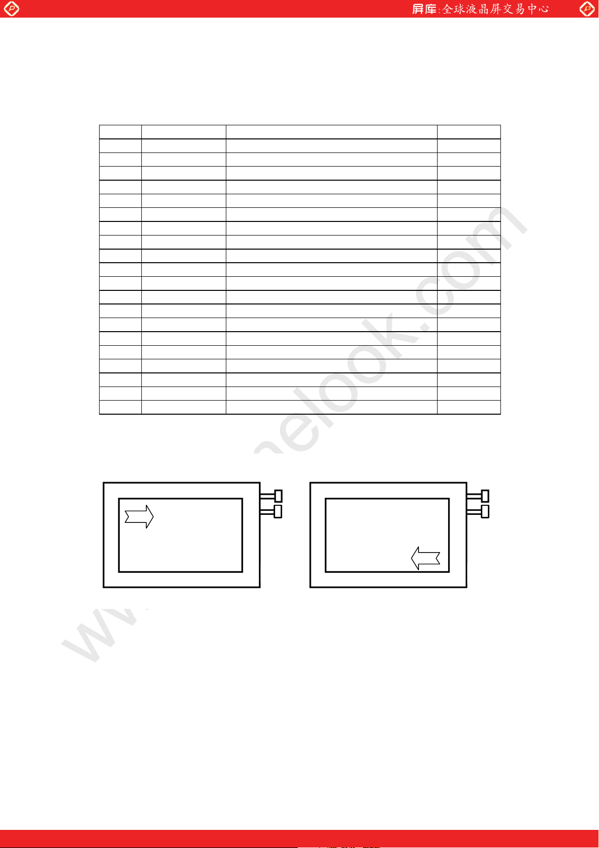
4. Input Terminals
4-1. TFT-LCD panel driving
CN1 (LVDS signals, +3.3V DC power supply and Contorol signal)
Corresponding connector: DF14-20S-1.25C (Connector) [Hirose electric.,Ltd]
DF14-2628SCF (Terminal) [Hirose electric.,Ltd]
Pin No. Symbol Function Remark
1 VCC +3.3V power supply
2 VCC +3.3V power supply
3 GND
4 GND
5 RXIN0- Differential data input, CH0 (negative) LVDS signal
6 RXIN0+ Differential data input, CH0 (positive) LVDS signal
7 GND
8 RXIN1- Differential data input, CH1 (negative) LVDS signal
9 RXIN1+ Differential data input, CH1 (positive) LVDS signal
10 GND
11 RXIN2- Differential data input, CH2 (negative) LVDS signal
12 RXIN2+ Differential data input, CH2 (positive) LVDS signal
13 GND
14 RXCLK IN- Differential clock input (negative) LVDS signal
15 RXCLK IN+ Differential clock input (positive) LVDS signal
16 GND
17 RXIN3- Differential data input, CH3 (negative) LVDS signal
18 RXIN3+ Differential data input, CH3 (positive) LVDS signal
19 RL/UD Horizontal/Vertical display mode select signal [Note1]
20 LVDS_SET LVDS_SET [Note2]
www.panelook.com
LD-19X11A-3
[Note 1]
RL/UD = Low RL/UD = High
[Note 2] Relation between LVDS signals and actual data shows below section (4-2)
One step solution for LCD / PDP / OLED panel application: Datasheet, inventory and accessory!
www.panelook.com
Page 6
Global LCD Panel Exchange Center
(
)
(
)
(
)
(
)
(
)
(
)
(NA)
(NA)
(NA)
(NA)
(
)
(
)
(
)
(
)
(
)
(
)
(NA)
(NA)
www.panelook.com
LD-19X11A-4
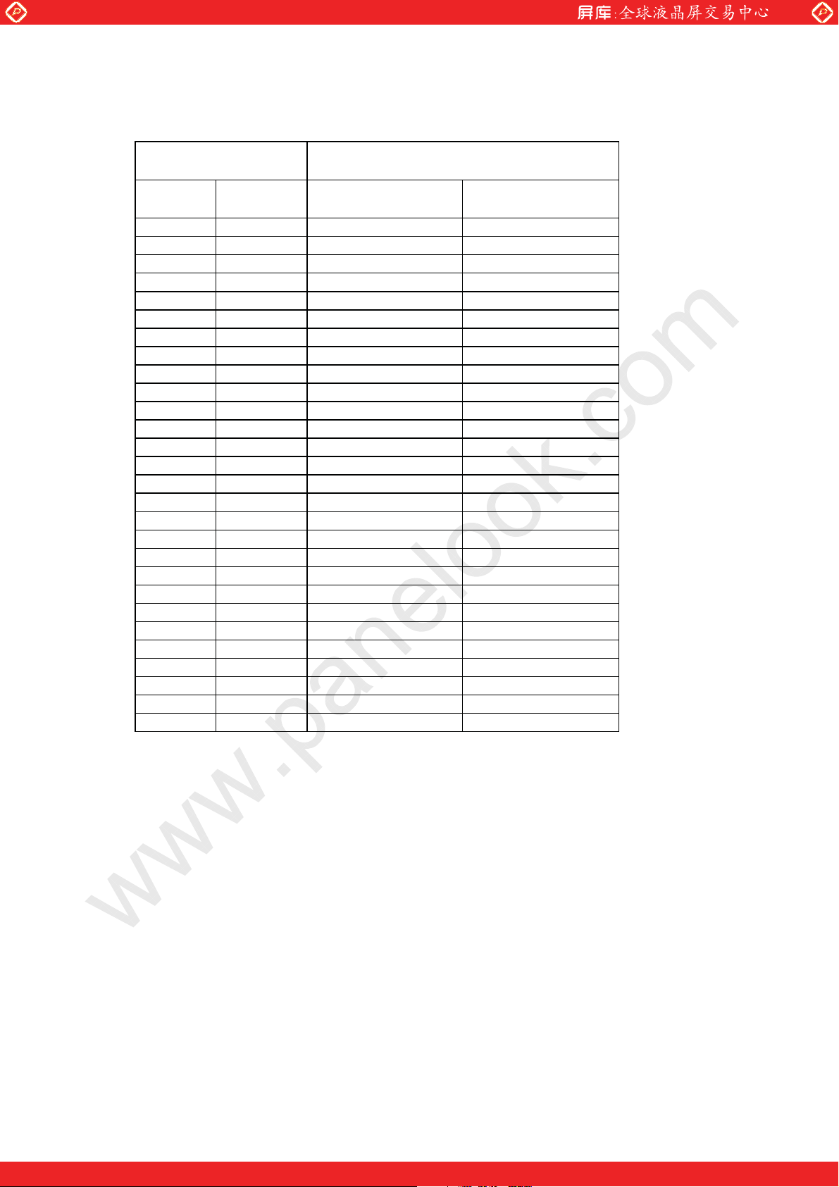
4-2
Data Mapping
1) 8 bit input
note2】pin assignment with LVDS_SET pin (Thine:THC63LVDM83R)
【
Transmitter 20pin LVDS_SET
Pin No Data =L (GND) or Open =H (3.3V)
51 TA0 R0
52 TA1 R1 R3
54 TA2 R2 R4
55 TA3 R3 R5
56 TA4 R4 R6
3 TA5 R5 R7
4 TA6 G0
6 TB0 G1 G3
7 TB1 G2 G4
11 TB2 G3 G5
12 TB3 G4 G6
14 TB4 G5 G7
15 TB5 B0
19 TB6 B1 B3
20 TC0 B2 B4
22 TC1 B3 B5
23 TC2 B4 B6
24 TC3 B5 B7
27 TC4
28 TC5
30 TC6 DE DE
50 TD0 R6 R0
2 TD1 R7
8 TD2 G6 G0
10 TD3 G7
16 TD4 B6 B0
18 TD5 B7
25 TD6
LSB
LSB
LSB
MSB
MSB
MSB
R2
MSB
G2
MSB
B2
MSB
LSB
R1
LSB
G1
LSB
B1
One step solution for LCD / PDP / OLED panel application: Datasheet, inventory and accessory!
www.panelook.com
Page 7
Global LCD Panel Exchange Center
NAN
NAN
play
N
NAN
NAN
play
N
www.panelook.com
LD-19X11A-5
< LVDS_SET = L or Open >
RXCKIN
RXCKIN-
RXIN0+
RXIN0-
RXIN1+
RXIN1-
RXIN2+
RXIN2-
RXIN3+
RXIN3-
DE: Dis
A: Not Available
Enable
1 cycle
G0 R5 R4 R3 R2 R1 R0 R0R1 G0
B1 B0 G5 G4 G3 G2 G1 G1G2 B1
DE B5 B4 B3 B2 B2B3 DE
A
B7 B6 G7 G6 R7 R6 R6R7
A
< LVDS_SET = H >
RXCKIN
RXCKIN-
RXIN0+
RXIN0-
RXIN1+
RXIN1-
RXIN2+
RXIN2-
RXIN3+
RXIN3-
1 cycle
G2 R7 R6 R5 R4 R3 R2 R2R3 G2
B3 B2 G7 G6 G5 G4 G3 G3G4 B3
DE B7 B6 B5 B4 B4B5 DE
A
B1 B0 G1 G0 R1 R0 R0R1
A
DE: Dis
Enable
A: Not Available
One step solution for LCD / PDP / OLED panel application: Datasheet, inventory and accessory!
www.panelook.com
Page 8

Global LCD Panel Exchange Center
)
)
)
)
)
)
(NA)
(NA)
(NA)
NAN
play
N
2) 6 bit input
note2】pin assignment with LVDS_SET pin (Thine:THC63LVDM83R)
【
Transmitter 20pin LVDS_SET
Pin No Data =L (GND) or Open =H (3.3V)
www.panelook.com
LD-19X11A-6
51 TA0
52 TA1
54 TA2
55 TA3
56 TA4
3 TA5
4 TA6
6 TB0
7 TB1
11 TB2
12 TB3
14 TB4
15 TB5
19 TB6
20 TC0
22 TC1
23 TC2
24 TC3
27 TC4
28 TC5
30 TC6
50 TD0
2 TD1
8 TD2
10 TD3
16 TD4
18 TD5
25 TD6
−
−
−
−
−
−
−
−
−
−
−
−
−
−
−
−
−
−
−
−
−
−
−
−
−
−
−
−
R0(LSB
R1
R2
R3
R4
R5(MSB
G0 (LSB
G1
G2
G3
G4
G5 (MSB
B0(LSB
B1
B2
B3
B4
B5(MSB
DE
GND
GND
GND
GND
GND
GND
RXCKIN
RXCKIN-
RXIN0+
RXIN0-
RXIN1+
RXIN1-
RXIN2+
RXIN2-
DE: Dis
Enable
A: Not Available
1 cycle
G0 R5 R4 R3 R2 R1 R0 R0R1 G0
B1 B0 G5 G4 G3 G2 G1 G1G2 B1
DE B5 B4 B3 B2 B2B3 DE
A
One step solution for LCD / PDP / OLED panel application: Datasheet, inventory and accessory!
www.panelook.com
Page 9

Global LCD Panel Exchange Center
㽲
㽳
t
㽴
R
K
,B7,
R
K
,B1,
R
K
www.panelook.com
4-3 Interface block diagram LD-19X11A-7
(Computer side)
8Bit䇭Mode
LVDS_SET=L (20 pin=GND or OPEN)
Controller
7
TA 0 - 6
R0-R5,G0
G1-G5,B0,B1
B2-B5, NA,NA,DE
R6,R7,G6,G7,
NA
B6
C
䇭Mode
8Bi
LVDS_SET=H (20 pin=3.3[V])
7
7
7
TB 0 - 6
TC 0 - 6
TD 0 - 6
CLK IN
THC63LVDM83
TTL PARALLEL-TO-LVDS
PLL
RXIN0+(6)
RXIN0-(5)
RXIN1+(9)
RXIN1-(8)
RXIN2+(12)
RXIN2-(11)
RXIN3+(18)
RXIN3-(17)
RXCKIN+(15)
RXCKIN-(14)
(TFT-LCD side)
Single LVDS interface contained in a control
LVDS-TO-PARALLEL TTL
PLL
RA 0 - 6
RB 0 - 6
RC 0 - 6
RD 0 - 6
CK OUT
Internal circuits
Controller
7
R2-R7,G2
G3-G7,B2,B3
B4-B7, NA,NA,DE
7
7
7
R0,R1,G0,G1,
NA
B0
C
6Bit䇭Mode
LVDS_SET=H (20 pin=3.3[V])
Controller
7
R0-R5,G0
G1-G5,B0,B1
B2-B5, NA,NA,DE
ALL NA
7
7
7
TA 0 - 6
TB 0 - 6
TC 0 - 6
TD 0 - 6
CLK IN
TA 0 - 6
TB 0 - 6
TC 0 - 6
TD 0 - 6
THC63LVDM83
TTL PARALLEL-TO-LVDS
PLL
THC63LVDM83
TTL PARALLEL-TO-LVDS
RXIN0+(6)
RXIN0-(5)
RXIN1+(9)
RXIN1-(8)
RXIN2+(12)
RXIN2-(11)
RXIN3+(18)
RXIN3-(17)
RXCKIN+(15)
RXCKIN-(14)
RXIN0+(6)
RXIN0-(5)
RXIN1+(9)
RXIN1-(8)
RXIN2+(12)
RXIN2-(11)
RXIN3+(18)
RXIN3-(17)
Single LVDS interface contained in a control IC
LVDS-TO-PARALLEL TTL
PLL
Single LVDS interface contained in a control IC
LVDS-TO-PARALLEL TTL
RA 0 - 6
RB 0 - 6
RC 0 - 6
RD 0 - 6
CK OUT
RA 0 - 6
RB 0 - 6
RC 0 - 6
RD 0 - 6
Internal circuits
Internal circuits
C
One step solution for LCD / PDP / OLED panel application: Datasheet, inventory and accessory!
CLK IN
PLL
RXCKIN+(15)
RXCKIN-(14)
PLL
CK OUT
www.panelook.com
Page 10

Global LCD Panel Exchange Center
4-4. Backlight driving
CN2 ,CN3
Used connector: BHR-02 (8.0) VS-1N (JST)
Corresponding connector: SM02 (8.0) B-BHS-1R-TB (JST)
SM02 (8.0) B-BHS-1-TB (JST)
Connector
No.
Pin No. Symbol function
1 V
CN2,3
2 V
5. Absolute Maximum Ratings
Parameter Symbol Condition Pin name Ratings Unit Remark
supply voltage Vcc Ta=25 oC
Input voltage
VI1 Ta=25oC
VI2 Ta=25oC
Lump input voltage V
HIGH
Storage temperature Tstg Operating temperature Topa panel
[Note1] Humidity: 95%RH Max. at Ta=<40oC.
Maximum wet-bulb temperature at 39
No condensation.
[Note2] A high voltage should be not able to be continued when the lamp doesn't light
HIGH
LOW
-
surface
www.panelook.com
Power supply for lamp
(High voltage side)
Power supply for lamp
(Low voltage side)
Vcc
RXINi-/+(i= 0,1,2,3)
RXCLK IN-/+
RL/UD, SELLVDS
V
(CN2,CN3)
HIGH
-
-
o
C or less at Ta>40 oC.
LD-19X11A-8
FL Cable color
CN2 CN3
White Pink
Gray White
-0.3 to 4.0 V [Note1,4]
-0.3 to Vcc+0.3 V
-0.3 to Vcc+0.3 V
0 to +2000 Vrms [Note1,2]
-30 to +75
0 to +70
o
C [Note1]
o
C [Note1,3]
[Note3] When used on condition of Operating temperature [65
℃≦
T
OPA
<70℃
],
degradation of display grace, such as screen stain etc, may be caused.
[Note4] Please use the one of 2A or more in current capacity about the power-supply voltage.
One step solution for LCD / PDP / OLED panel application: Datasheet, inventory and accessory!
www.panelook.com
Page 11

Global LCD Panel Exchange Center
V
V
www.panelook.com
LD-19X11A-9
6. Electrical Characteristics
o
6-1.TFT-LCD panel driving Ta=+25
C
Parameter Symbol Min. Typ. Max. Unit Remark
Supply voltage Vcc +3.0 +3.3 +3.6 V [Note4]
Current dissipation Vcc=+3.3V Icc - 290 380 mA [Note5]
Input voltage range LVDS signal VL 0 - 2.4 V [Note3]
Permissive input ripple voltage Vcc=+3.3V VRP - - 100 mVp-p Vcc=+3.3V
V
Differential input
High V
threshold voltage Low V
Input voltage
Input current
Input impedance
(Differential input)
High VIH 2.1 - - [Note2]
Low V
High IOH - - 500
Low I
R
- -
TH
V
TL
IL
OL
T
CM
–100
- - 0.8
-10 - 10
- 100 -
- - mV [Note1]
CM
+100
mV
V
μ
μ
Ω
VCM=1.2V
VI2=+3.3V[Note2]
A
A
VI2=0V[Note2]
[Note1] VCM : Common mode voltage of LVDS driver [Note2]RL/UD,SELLVDS
[Note3]LVDS signals
[Note4]On-off conditions for supply voltage Vcc-dip conditions
2.7V
0.3V
cc
2.7V
0.3V 0.3V
Vcc
data
Back light
t2
t1
ON
t5
OFF
t3
t6
t4
td
OFF
Vmin
th
Vth:2.5V
Vmin:3.0V
0<t1≦10ms 0<t2≦10ms 1) Vth ≦ Vcc < Vmin
0<t3≦1s 1s≦t4 td
10ms
≦
300ms≦t5 200ms≦t6 2) Vcc<Vth
Vcc-dip conditions should also follow
the On-off conditions for supply voltage
Please use DE signal by the Lo start.
・
Please do not input Vsync/Hsync to this module,it is recommend to be used by the pull-down
・
It is recommended to consider some timing difference between LVDS input and Backlight input as shown above.
・
If the Backlight lights on before LCD starting, or if the Backlight is kept on after LCD stopping, the screen may
look white for a moment or abnormal image may be displayed. This is caused by variation in output signal from
timing generator at LVDS input on or off. It does not cause the damage to the LCD module
[Note 5] Typical current situation : 253-gray-bar pattern.
(Vcc=+3.3V,fck=40MHz,Ta=+25℃)
The explanation of each gray scale
RGB
GS0
RGB
GS4
RGB
GS8
....
RGB
GS251
RGB
GS252
is described below section 8
One step solution for LCD / PDP / OLED panel application: Datasheet, inventory and accessory!
www.panelook.com
Page 12

Global LCD Panel Exchange Center
6-2. Backlight driving
The backlight system is an edge-lighting type with single CCFT (Cold Cathode Fluorescent Tube).
The characteristics of single lamp are shown in the following table.
Parameter Symbol Min. Typ. Max. Unit Remark
Lamp current range IL 3.0 6.5 7.5 mArms [Note1]
Lamp voltage VL - 465 540 Vrms
Lamp power consumption PL - 3.0 - W [Note2]
Lamp frequency FL 40 - 70 kHz [Note3]
Kick-off voltage Vs - - 1100 Vrms
Lamp life time L
[Note1] Lamp current is measured with current meter for high frequency as shown below.
㪚㪥㪉㪃㪊䋺㪈㫇㫀㫅
㪤㫆㪻㫌㫃㪼
㪚㪥㪉㪃㪊䋺㪉㫇㫀㫅
L
www.panelook.com
50000
(Lump unit)
-
A
〜
- - IL=6.5mA [Note5]
20000
(Module)
V
〜
hour
-
Inverter output voltage
LD-19X11A-10
Ta=+25℃,IL=6.5mArms
Inverter output voltage
[Reference]
Ballast capacitor
㪠㫅㫍㪼㫉㫋㪼㫉
V
Trance output voltage
〜
Ta=0
℃
V
[Note2] Reference value by one fluorescent lamp calculation (I
It is assumed the value that doesn't contain the loss of the inverter. ( I
)
×
L
L
= 6.5mArms )
L
[Note3] Lamp frequency may produce interference with horizontal synchronous frequency, andthis may cause
beat on the display. Therefore lamp frequency shall be detached as much as possible from the
horizontal synchronous frequency and from the harmonics of horizontal synchronous to avoid
interference.
[Note4] The value of the trans output side in the inverter of ballast capacitor 27pF is described.
Lighting beginning voltage might rise according to the state of the user cabinet mounting, and please
set the open-circuit voltage of the inverter so as not to generate the lighting failure while real used.
The voltage above this value should be applied to the lamp for more than 1 second to start-up.
Otherwise the lamp may not be turned on.
[Note5] Since lamp is consumables, the life time written above is referencial value and it is not guaranteed in
this specification.
Lamp life time is defined that it applied either ① or ② under this condition
o
(Continuous turning on at Ta=25
Brightness becomes 50% of the original value under standard condition.
①
Kick-off voltage at Ta=0
②
C, IL=6.5mArms)
o
C exceeds maximum value,1100Vrms.
In case of operating under lower temp environment, the lamp exhaustion is accelerated and the
brightness becomes lower. (Continuous operating under for around 1 month under lower temp
condition may reduce the brightness to half of the original brightness.)
In case of such usage under lower temp environment, periodical lamp exchange is recommended.
[Note] Please synchronize the lighting frequency and the phase of the lamp of the same connector.
There is a possibility to exceed ratings of the connector when not synchronizing.
One step solution for LCD / PDP / OLED panel application: Datasheet, inventory and accessory!
www.panelook.com
Page 13

Global LCD Panel Exchange Center
[Note] The performance of the backlight, for example life time or brightness, is much influenced by the
characteristics of the DC-AC inverter for the lamp. When you design or order the inverter, please make
sure that a poor lighting caused by the mismatch of the backlight and the inverter (miss-lighting, flicker,
etc.) never occur. When you confirm it, the module should be operated in the same condition as it is
installed in your instrument.
Be sure to use a back light power supply with the safety protection circuit such as the detection
circuit for the excess voltage, excess current and or electric discharge waveform.
Be sure to use the detect circuit by which one side of the CCFT lamps can be controlled
independently. Otherwise, when one side of the CCFT is open, the excess current may possibly
be applied to the other side of the lamp.
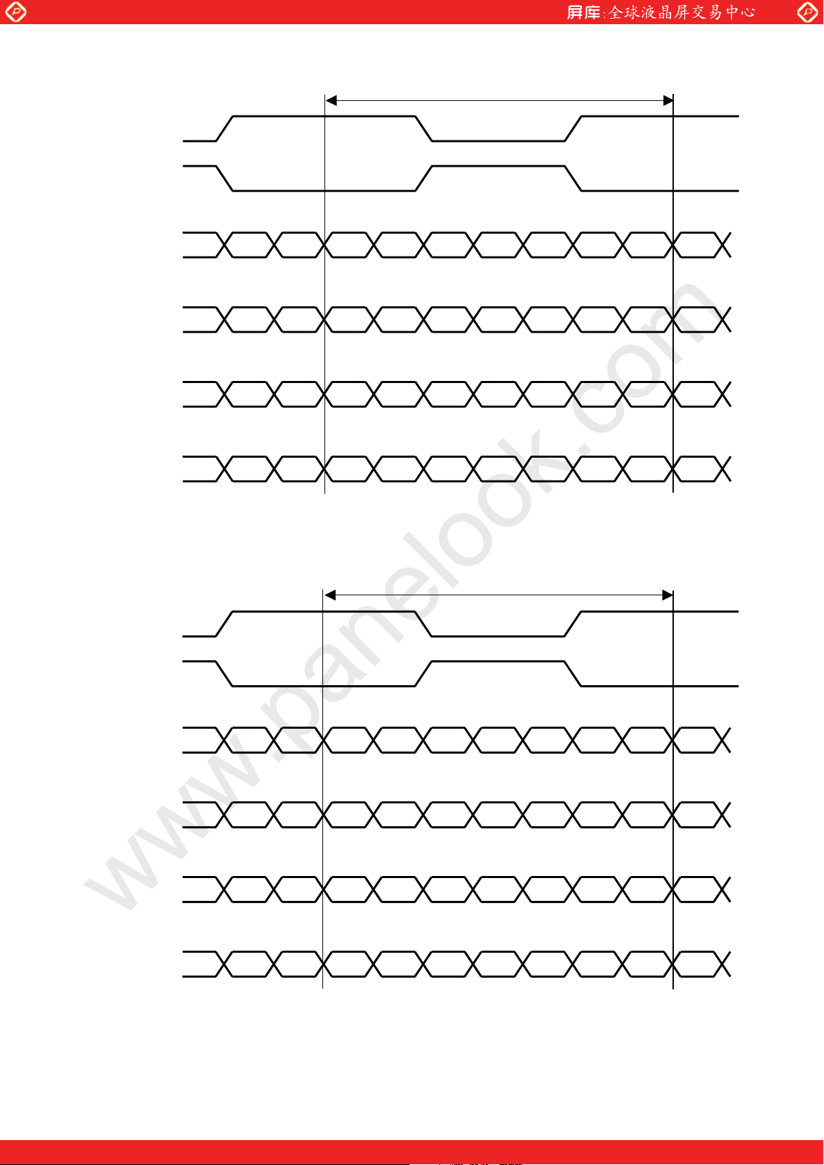
7. Timing characteristics of input signals
7-1. Timing characteristics
Parameter Symbol Min. Typ. Max. Unit
Clock signal Frequency 1/Tc 35 40 42 MHz
Horizontal period TH 832 1056 1395 clock
www.panelook.com
LD-19X11A-11
20.8 26.4 39.9 μs
ENAB signal
Horizontal period (High) THd
TV 628 666 798 line
800 800 800 clock
Vertical period
−
17.6
−
Vertical period (High) TVd 600 600 600 line
Note】 In case of using the long vertical period, the deterioration of display quality, flicker etc. may occur.
【
TH
THd
ENAB
DATA
12
(R,G,B)
Tc
ms
1 2 600
599
ENAB
TVd
TV
One step solution for LCD / PDP / OLED panel application: Datasheet, inventory and accessory!
www.panelook.com
Page 14

Global LCD Panel Exchange Center
7-2. Input Data Signals and Display Position on the screen
Display position of input data
www.panelook.com
( H , V
)
LD-19X11A-12
UP
D(1,1)
D(1,2)
D(1,3)
D(1,600)
D(2,1)
D(2,2)
D(3,1) D(800,1)
R G B
D(800,600)
One step solution for LCD / PDP / OLED panel application: Datasheet, inventory and accessory!
www.panelook.com
Page 15

Global LCD Panel Exchange Center
www.panelook.com
8. Input Signals, Basic Display Colors and Gray Scale of Each Color
8-1 8bit input
Colors &
Gray scale
Gray
R0 R1 R2 R3 R4 R5 R6 R7 G0 G1 G2 G3 G4 G5 G6 G7 B0 B1 B2 B3 B4 B5 B6 B7
LD-19X11A-13
Data signal
Black
Blue
Basic Color Gray Scale of Red
Green
Cyan
Red
Magenta
Yellow
White
Black GS0 0 0 0 0 0 0 0 0 0 0 0 0 0 0 0 0 0 0 0 0 0 0 0 0
GS1 1 0 0 0 0 0 0 0 0 0 0 0 0 0 0 0 0 0 0 0 0 0 0 0
×
Darker GS2 0 1 0 0 0 0 0 0 0 0 0 0 0 0 0 0 0 0 0 0 0 0 0 0
×È È È È
ØÈ È È È
Brighter GS250 1 0 0 1 1 1 1 1 0 0 0 0 0 0 0 0 0 0 0 0 0 0 0 0
GS251 1 1 0 1 1 1 1 1 0 0 0 0 0 0 0 0 0 0 0 0 0 0 0 0
Ø
Red GS252
Black GS0 0 0 0 0 0 0 0 0 0 0 0 0 0 0 0 0 0 0 0 0 0 0 0 0
Gray Scale of Green
GS1 0 0 0 0 0 0 0 0 1 0 0 0 0 0 0 0 0 0 0 0 0 0 0 0
×
Darker GS2 0 0 0 0 0 0 0 0 0 1 0 0 0 0 0 0 0 0 0 0 0 0 0 0
0 0 0 0 0 0 0 0 0 0 0 0 0 0 0 0 0 0 0 0 0 0 0 0
−
0 0 0 0 0 0 0 0 0 0 0 0 0 0 0 0
−
0 0 0 0 0 0 0 0
−
0 0 0 0 0 0 0 0
−
−XX
−XX
−XX
−XX
XX
1 1 1 1 1 1 0 0 0 0 0 0 0 0 0 0 0 0 0 0 0 0
1 1 1 1 1 1 0 0 0 0 0 0 0 0
1 1 1 1 1 1
1 1 1 1 1 1
1 1 1 1 1 1 0 0 0 0 0 0 0 0 0 0 0 0 0 0 0 0
XX
XX
XX
XX
1111110 0 0 0 0000
111111
1111110 0 0 0 0000
111111
XX
XX
XX
XX
1 1 1 1 1 1
1 1 1 1 1 1
1 1 1 1 1 1
1 1 1 1 1 1
×È È È È
ØÈ È È È
Brighter GS250 0 0 0 0 0 0 0 0 1 0 0 1 1 1 1 1 0 0 0 0 0 0 0 0
GS251 0 0 0 0 0 0 0 0 1 1 0 1 1 1 1 1 0 0 0 0 0 0 0 0
Ø
Green GS252 0 0 0 0 0 0 0 0
Black GS0 0 0 0 0 0 0 0 0 0 0 0 0 0 0 0 0 0 0 0 0 0 0 0 0
Gray Scale of Blue
GS1 0 0 0 0 0 0 0 0 0 0 0 0 0 0 0 0 1 0 0 0 0 0 0 0
×
Darker GS2 0 0 0 0 0 0 0 0 0 0 0 0 0 0 0 0 0 1 0 0 0 0 0 0
×È È È È
ØÈ È È È
Brighter GS250 0 0 0 0 0 0 0 0 0 0 0 0 0 0 0 0 1 0 0 1 1 1 1 1
GS251 0 0z 0 0 0 0 0 0 0 0 0 0 0 0 0 0 1 1 0 1 1 1 1 1
Ø
Blue GS252 0 0 0 0 0 0 0 0 0 0 0 0 0 0 0 0
XX
1111110 0 0 0 0000
XX
1 1 1 1 1 1
0 : Low level voltage, 1 : High level voltage X:Don’t care
Each basic color can be displayed in 253 gray scales from 8 bit data signals. According to the combination of
total 24 bit data signals, the 16-million-color display can be achieved on the screen.
One step solution for LCD / PDP / OLED panel application: Datasheet, inventory and accessory!
www.panelook.com
Page 16

Global LCD Panel Exchange Center
8-2 6bit input
Colors &
Gray scale
Gray
scale
R0 R1 R2 R3 R4 R5 G0 G1 G2 G3 G4 G5 B0 B1 B2 B3 B4 B5
− 0 0 0 0 0 0 0 0 0 0 0 0 0 0 0 0 0 0
Black
Blue
Basic Color Gray Scale of Red
Green
Cyan
Red
Magenta
Yellow
− 0 0 0 0 0 0 0 0 0 0 0 0 1 1 1 1 1 1
− 0 0 0 0 0 0 1 1 1 1 1 1 0 0 0 0 0 0
− 0 0 0 0 0 0 1 1 1 1 1 1 1 1 1 1 1 1
− 1 1 1 1 1 1 0 0 0 0 0 0 0 0 0 0 0 0
− 1 1 1 1 1 1 0 0 0 0 0 0 1 1 1 1 1 1
− 1 1 1 1 1 1 1 1 1 1 1 1 0 0 0 0 0 0
− 1 1 1 1 1 1 1 1 1 1 1 1 1 1 1 1 1 1
www.panelook.com
LD-19X11A-14
Data signal
White
Black
×
Darker
×
Ø
Brighter
Ø
Red
Black
Gray Scale of Green
×
Darker
×
Ø
Brighter
Ø
GS0 0 0 0 0 0 0 0 0 0 0 0 0 0 0 0 0 0 0
GS1 1 0 0 0 0 0 0 0 0 0 0 0 0 0 0 0 0 0
GS2 0 1 0 0 0 0 0 0 0 0 0 0 0 0 0 0 0 0
ÈÈ È È
ÈÈ È È
GS61 1 0 1 1 1 1 0 0 0 0 0 0 0 0 0 0 0 0
GS62 0 1 1 1 1 1 0 0 0 0 0 0 0 0 0 0 0 0
GS63 1 1 1 1 1 1 0 0 0 0 0 0 0 0 0 0 0 0
GS0 0 0 0 0 0 0 0 0 0 0 0 0 0 0 0 0 0 0
GS1 0 0 0 0 0 0 1 0 0 0 0 0 0 0 0 0 0 0
GS2 0 0 0 0 0 0 0 1 0 0 0 0 0 0 0 0 0 0
ÈÈ È È
ÈÈ È È
GS61 0 0 0 0 0 0 1 0 1 1 1 1 0 0 0 0 0 0
GS62 0 0 0 0 0 0 0 1 1 1 1 1 0 0 0 0 0 0
GS63 0 0 0 0 0 0 1 1 1 1 1 1 0 0 0 0 0 0
Green
Black
Gray Scale of Blue
×
Darker
×
Ø
Brighter
Ø
GS0 0 0 0 0 0 0 0 0 0 0 0 0 0 0 0 0 0 0
GS1 0 0 0 0 0 0 0 0 0 0 0 0 1 0 0 0 0 0
GS2 0 0 0 0 0 0 0 0 0 0 0 0 0 1 0 0 0 0
ÈÈ È È
ÈÈ È È
GS61 0 0 0 0 0 0 0 0 0 0 0 0 1 0 1 1 1 1
GS62 0 0 0 0 0 0 0 0 0 0 0 0 0 1 1 1 1 1
GS63 0 0 0 0 0 0 0 0 0 0 0 0 1 1 1 1 1 1
0 : Low level voltage, 1 : High level voltage.
Each basic color can be displayed in 64 gray scales from 6 bit data signals. According to the combination of
total 18 bit data signals, the 262,144-color display can be achieved on the screen.
One step solution for LCD / PDP / OLED panel application: Datasheet, inventory and accessory!
www.panelook.com
Page 17

Global LCD Panel Exchange Center
9. Optical Characteristics9. Optical Characteristics
www.panelook.com
LD-19X11A-15
Ta=+25℃, Vcc =+3.3V
Parameter Symbol Condition Min. Typ. Max. Unit Remark
Viewing
angle
range
Horizontal
Vertical
21,θ22
θ
θ
θ
11
12
CR≧10
60 70
35 50
55 60
- Deg.
- Deg.
- Deg.
Optimum
Contrast ratio
CR
viewing
250 400 - - [Note2,4]
angle
r - 10 - ms
τ
[Note3]
Response time
White
Red
d - 25 - ms
τ
x
y
x
y
x
0.283 0.313 0.343
0.299 0.329 0.359
0.618 0.648 0.678
0.306 0.336 0.366
0.253 0.283 0.313
-Chromaticity of
-
-Chromaticity of
-
-Chromaticity of
[Note3]
[Note4]
θ=0°
Green
Blue
y
x
y
0.582 0.612 0.642
0.114 0.144 0.174
0.052 0.082 0.112
-
-Chromaticity of
-
[Note4]
2
Luminance of white Y
White Uniformity
The measurement shall be executed 30 minutes after lighting at rating.
※
The optical characteristics shall be measured in a dark room or equivalent state with the method shown in Fig.2 below.
δ
L
w
Photodetector(EZ−CONTRAST
260 330
−−
)
−
1.25
Photodetector
Response Time(BM−5A)
Contrast ratio/ Luminance /Chromaticity(SR−3)
cd/m
−
F = 60KHz
I
= 6.5mArms
L
[Note5]
400mm
Center of screen
(θ=
0
°)
Field=1
Center of screen
°
(θ=0°)
TFT−LCD Module
Fig2-1 Viewing angle measurement method
Fig2 Optical characteristics measurement method
Fig2-2 Luminance/Contrast ratio/Response time/Chromaticity
measurement method
TFT−LCD Module
One step solution for LCD / PDP / OLED panel application: Datasheet, inventory and accessory!
www.panelook.com
Page 18

Global LCD Panel Exchange Center
0
www.panelook.com
LD-19X11A-16
[Note1]Definitions of viewing angle range:
T
22
T
12
Normal
T
11
T
21
6 o’clock
[Note2] Definition of contrast ratio:
The contrast ratio is defined as the following.
Luminance (brightness) with all pixels white
Contrast Ratio (CR)
=
Luminance (brightness) with all pixels black
[Note3] Definition of response time:
The response time is defined as the following figure and shall be measured by switching the input signal for
"black" and "white".
White White Black
100
%
90
%
10
%
Photodetector Output
(Relative Value)
W
d
W
r
[Note4] This shall be measured at center of the screen.
[Note5] Definition of white uniformity:
White uniformity is defined as the following with five measurements(A〜E).
Maximum Luminance of five points (brightness)
δw=
Minimum Luminance of five points (brightness)
Time
pixel 600 200 400
A
C
B
D
E
150
300
450
pixel
One step solution for LCD / PDP / OLED panel application: Datasheet, inventory and accessory!
www.panelook.com
Page 19

Global LCD Panel Exchange Center
10.Handling Precautions
a) Be sure to turn off the power supply when inserting or disconnecting the cable.
b) Be sure to design the cabinet so that the module can be installed without any extra stress such as warp or
twist.
c) Since the front polarizer is easily damaged, pay attention not to scratch it.
d) Wipe off water drop immediately. Long contact with water may cause discoloration or spots.
e) When the panel surface is soiled, wipe it with absorbent cotton or other soft cloth.
f) Since the panel is made of glass, it may break or crack if dropped or bumped on hard surface.
Handle with care.
g) Since CMOS LSI is used in this module, take care of static electricity and injure the human earth when
handling.Observe all other precautionary requirements in handling components.
h) Since there is a circuit board in the module back, stress is not added at the time of a design assembly.
Please make it like. If stress is added, there is a possibility that circuit parts may be damaged.
i) Protection film is attached to the module surface to prevent it from being scratched .
Peel the film off slowly , just before the use, with strict attention to electrostatic charges.
Blow off 'dust' on the polarizer by using an ionized nitrogen.
j) The polarizer surface on the panel is treated with Anti-Glare for low reflection. In case of attaching
protective board over the LCD, be careful about the optical interface fringe etc. which degrades display
quality.
k) Do not expose the LCD panel to direct sunlight. Lightproof shade etc. should be attached when LCD panel
is used under such environmentl
l) Connect GND to 4 place of mounting holes to stabilize against EMI and external noise.
m) There are high voltage portions on the backlight and very dangerous. Careless touch may lead to electrical
shock. When exchange lamps or service, turn off the power without tail.
n) When handling LCD modules and assembling them into cabinets, please be noted that long-term storage in
the environment of oxidization or deoxidization gas and the use of such materials as reagent,solvent,
adhesive, resin, etc. which generate these gasses, may cause corrosion and discoloration of the LCD modules.
o) Cold cathode fluorescent lamp in LCD panel contains a small amount of mercury, please follow local
ordinances or regulations for disposal.
p) Be careful of a back light lead not to pull by force at the time of the wiring to an inverter, or line processing.
q) When install LCD modules in the cabinet, please tighten with “torque=0.294±0.02N・m(3.0±0.2kgf・cm)”.
www.panelook.com
LD-19X11A-17
One step solution for LCD / PDP / OLED panel application: Datasheet, inventory and accessory!
www.panelook.com
Page 20

Global LCD Panel Exchange Center
11. Packing form
Piling number of cartons MAX. 5
Package quantity in one carton 10pcs
Carton size
www.panelook.com
LD-19X11A-18
395(W)×275(H)×350(D) mm
Total mass of one carton filled
8000g
with full modules
Packing form is shown
Fig.3
12. Reliability test items
No. Test item Conditions Remark
1 High temperature
Ta=75℃ 240h
storage test
2 Low temperature
Ta= -30℃ 240h
storage test
3 High temperature
& high humidity operation test
4 High temperature operation test
5 Low temperature operation test
6 Vibration test
(non- operating)
Ta=40℃ ; 95%RH 240h
(No condensation)
T=70℃ (panel surface) 240h
Ta= 0℃ (panel surface) 240h
Frequency: 10〜57Hz/Vibration width (one side):0.075mm
: 57〜500Hz/Gravity:9.8m/s
2
Sweep time : 11 minutes
Test period : 3 hours (1 hour for each direction of X,Y,Z)
7 Shock test
(non- operating)
Max. gravity : 490m/s
Pulse width : 11ms, half sine wave
2
Direction : ±X,±Y,±Z once for each direction.
8 ESD test
Contact discharge (
150pF 330
Ω
)
non-operating = ±10kV, operating = ±8kV
Atmospheric discharge (
150pF 330
Ω
)
non-operating = ±20kV, operating = ±15kV
[Result Evaluation Criteria]
Under the display quality test conditions with normal operation state, these shall be no change
which may affect practical display function. (normal operation state:Temperature:15〜35℃,
Humidity:45〜75%, Atmospheric pressure:86〜106kpa)
One step solution for LCD / PDP / OLED panel application: Datasheet, inventory and accessory!
www.panelook.com
Page 21

Global LCD Panel Exchange Center
13.Others
1) Lot number Label:
www.panelook.com
LD-19X11A-19
LQ0DZA0126
7X XXXXXX
2) Adjusting volume have been set optimally before shipment, so do not change any adjusted value.
If adjusted value is changed, the specification may not be satisfied.
3) Disassembling the module can cause permanent damage and should be strictly avoided.
4) Please be careful since image retention may occur when a fixed pattern is displayed for a long time.
Model No.
Lot No.
One step solution for LCD / PDP / OLED panel application: Datasheet, inventory and accessory!
www.panelook.com
Page 22

Global LCD Panel Exchange Center
LD-19X11A-20
www.panelook.com
One step solution for LCD / PDP / OLED panel application: Datasheet, inventory and accessory!
www.panelook.com
Page 23

Global LCD Panel Exchange Center
www.panelook.com
LD-19X11A-21
One step solution for LCD / PDP / OLED panel application: Datasheet, inventory and accessory!
www.panelook.com
 Loading...