.‘
i
PREPARED BY :
DATE
SHARP
SPECIFICATION
DEVICE SPECIFICATION for
Passive Matrix LCD Module
Mode 1 No.
SPEC No. L C 9 9 2 0 4
FILE No.
I SSUED FEB. 5.1999
PAGE 24 Pages
APPLICABLE DIVISION
N DUTY LCD DEVELOPMENT CENTEI
Z TFT DEVELOPMENT CENTER
iIl LCD PRODUCTS DEVELOPMEN
CENTER
i1 EL PRODUCT ION DEPT.
Cl CUSTOMER’S APPROVAL
DATE
Lid3201 921
Y. I noue
Depart d nt General Manager
Mobile LCD Department P.T Module
DUTY LCD Department Center
DUTY Liquid Crystal Display Group
SHARP Corporation
SPEC. No. MO0E.L No. .
RECORDS OF REVISION
LC99204
DOC. FIRST ISSUE
LY3201921
FEB. 5.1999
IDENT. DATA No.
DATE SPEC REVISED REF. PAGE SUMMARY CHECK
REVISED No. &
No. APPROVAL
. . . . . . . . . . . . . . . . . . . . . . . . . . . . . . . . . . . . . . . . . . . . . . . . . . . . . . . . . . . . . . . . . . . . . . . . . . . . . . . . . . . . . . . . . . . . . . . . . . . . . . . . . . . . . . . . . . . . . . . . .............
. . . . . . . . . . . . . . . . . . . . . . . . . . . . . . . . . . . . . . . . . . . . . . . . . . . . . . . . . . . . . . . . . . . . . . . . . . . . . . . . . . . . . . . . . . . . . . . . . . . . . . . . . . . . . . . . . . . . . . . . .............
. . . . . . . . . . . . . . . . . . . . . . . . . . . . . . . . . . . . . . . . . . . . . . . . . . . . . . . . . . . . . . . . . . . . . . . . . . . . . . . . . . . . . . . . . . . . . . . . . . . . . . . . . . . . . . . . . . . . . . . . .............
. . . . . . . . . . . . . . . . . . . . . . . . . . . . . . . . . . . . . . . . . . . . . . . . . . . . . . . . . . . . . . . . . . . . . . . . . . . . . . . . . . . . . . . . . . . . . . . . . . . . . . . . . . . . . . . . . . . . . . . . .............
. . . . . . . . . . . . . . . . . . . . . . . . . . . . . . . . . . . . . . . . . . . . . . . . . . . . . . . . . . . . . . . . . . . . . . . . . . . . . . . . . . . . . . . . . . . . . . . . . . . . . . . . . . . . . . . . . . . . . . . . .............
~........___....._...................................................................................................................
. . . . . . . . . . . . . . . . . . . . . . . . . . . . . . . . . . . . . . . . . . . . . . . . . . . . . . . . . . . . . . . . . . . . . . . . . . . . . . . . . . . . . . . . . . . . . . . . . . . . . . . . . . . . . ..--...................
. . . . . . . . . . . . . . . . . . . . . . . . . . . . . . . . . . . . . . . . . . . . . . . . . . . . . . . . . . . . . . . . . . . . . . . . . . . . . . . . . . . . . . . . . . . . . . . . . . . . . . . . . . . . . . . . . . . . . . . . ............
. . . . . . . . . . . . . . . . . . . . . . . . . . . . . . . . . . . . . . . . . . . . . . . . . . . . . . . . . . . . . . . . . . . . . . . . . . . . . . . . . . . . . . . . . . . . . . . . . . . . . . . . . . . . . ..-........-...........
. . . . . . . . . . . . . . . . . . . . . . . . . . . . . . . . . . . . . . . . . . . . . . . . . . . . . . . . . . . . . . . . . . . . . . . . . . . . . . . . . . . . . . . . . . . . . . . . . . . . . . . . . . . . . . . . . . . . . . . . ............
. . . . . . . . . . . . . . . . . . . . . . . . . . . . . . . . . . . . . . . . . . . . . . . . . . . . . . . . . . . . . . . . . . . . . . . . . . . . . . . . . . . . . . . . . . . . . . . . . . . . . . . . . . . . . . . . . . . . . . . . ............
. . . . . . ..__......_............................*......................................................................................
. . . . . . . . . . . . . . . . . . . . . . . . . . . . . . . . . . . . . . . . . . . . . . . . . . . . . . . . . . . . . . . . . . . . . . . . . . . . . . . . . . . . . . . . . . . . . . . . . . . . . . . . . . . . . ..---.....--.....---...
. . . . . . ..__..........................................................................................................................~
. . . . . . . . . . . . . . . . . . . . . . . . . . . . . . . . . . . . . . . . . . . . . . . . . . . . . . . . . . . . . . . . . . . . . . . . . . . . . . . . . . . . . . . . . . . . . . . . . . . . . . . . . . . . . . . ..-.....--....----.--.
. . . . . . . . . . . . . . . . . . . . . . . . . . . . . . . . . . . . . . . . . . . . . . . . . . . . . . . . . . . . . . . . . . . . . . . . . . . . . . . . . . . . . . . . . . . . . . . . . . . . . . . . . . . . . . . . . . . . . . . . .......--....
. . . . . . . . . . . . . . . . . . . . . . . . . . . . . . . . . . . . . . . . . . . . . . . . . . . . . . . . . . . . . . . . . . . . . . . . . . . . . . . . . . . . . . . . . . . . . . . . . . . . . . . . . . . . . . . . . . . . . . ..-.....---.--.
. . . . . . . . . . . . . . . . . . . . . . . . . . . . . . . . . . . . . . . . . . . . . . . . . . . . . . . . . . . . . . . . . . . . . . . . . . . . . . . . . . . . . . . . . . . . . . . . . . . . . . . . . . . . . . . . . . . . . ..--....----....
. . . . . . . . . . . . . . . . . . . . . . . . . . . . . . . . . . . . . . . . . . . . . . . . . . . . . . . . . . . . . . . . . . . . . . . . . . . . . . . . . . . . . . . . . . . . . . . . . . . . . . . . . . . . . . . ..-.....-......-.-....
. . . . . . . . . . . . . . . . . . . . . . . . . . . . . . . . . . . . . . . . . . . . . . . . . . . . . . . . . . . . . . . . . . . . . . . . . . . . . . . . . . . . . . . . . . . . . . . . . . . . . . . . . . . . . . . . . . . . . . . . . . . . . . . . . . . . .
. . . . . . . . . . . . . . . . . . . . . . . . . . . . . . . . . . . . . . . . . . . . . . . . . . . . . . . . . . . . . . . . . . . . . . . . . . . . . . . . . . . . . . . . . . . . . . . . . . . . . . . . ..*..........................
. . . . . . . . . . . . . . . . . . . . . . . . . . . . . . . . . . . . . . . . . . . . . . . . . . . . . . . . . . . . . . . . . . . . . . . . . . . . . . . . . . . . . . . . . . . . . . . . . . . . . . . . . . . . . . . . . . . . . . . . ............
. . . . . . . . . . . . . . . . . . . . . . . . . . ..-..................................................................................................-....
. . . . . . . . . . . . . . . . . . . . . . . . . . . . . . . . . . . . . . . . . . . . . . . . . . . . . . . . . . . . . . . . . . . . . . . . . . . . . . . . . . . . . . . . . . . . . . . . . . . . . . . . . . . . . . . . . . . . . . . . ............
. . . . . . . . . . . . . . . . . . . . . . . . ..---.......-..........................................................................................-...-
. . . . . . . .._.....................................................................................................................~....
--.................---.....--.......................................................................................,...............
SHARP
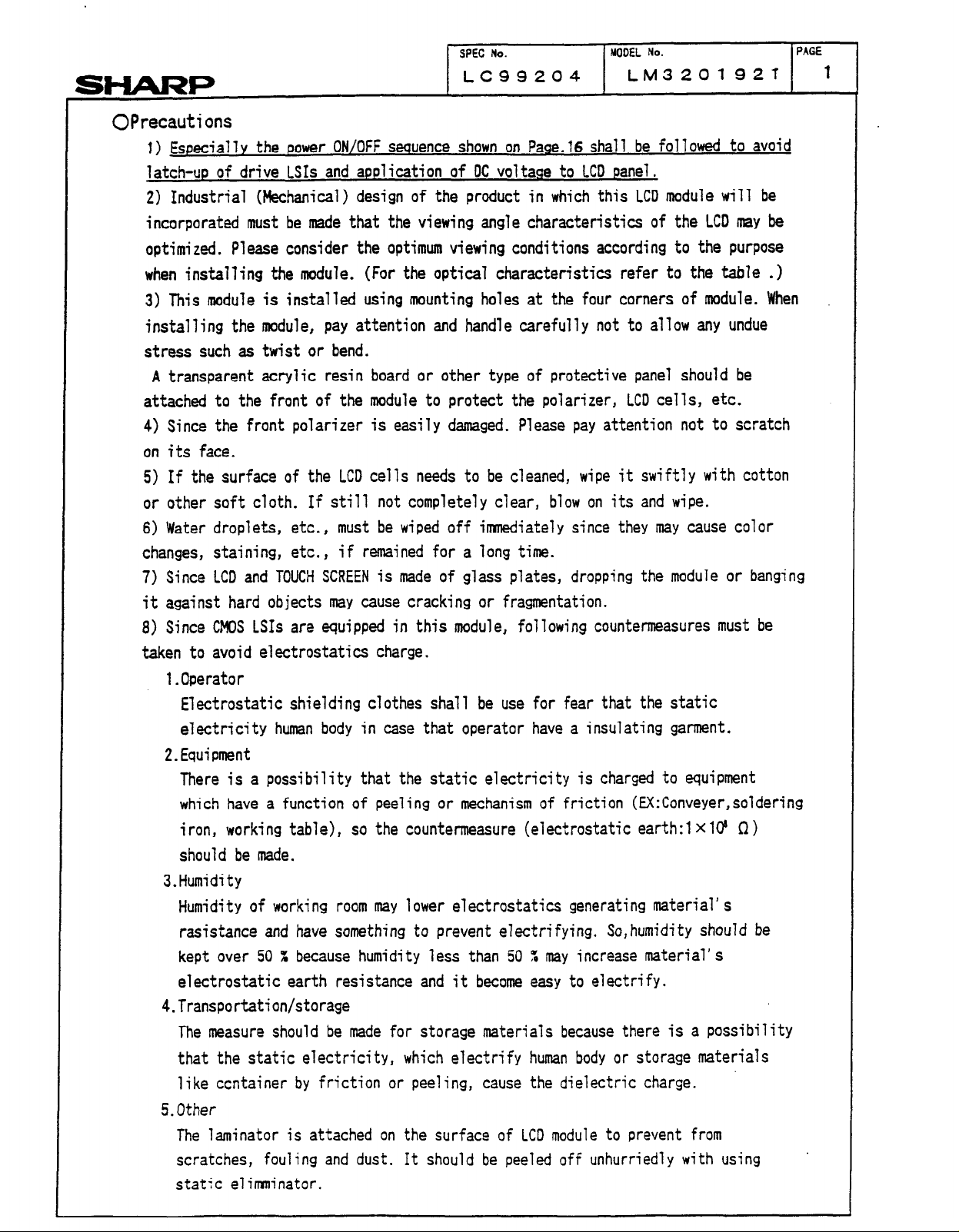
OPrecautions
1) EspeciaJJy the power ON/OFF sequence shown on Page.16 shall be followed to avoid
latch-up of drive LSIs and application of OC voltage to LCD panel.
2) Industrial (Mechanical) design of the
incorporated
optimized. Please consider the optimum viewing conditions according to the purpose
when installing the module. (For the optical characteristics refer to the table .)
3) This module is installed using mounting holes at the four corners of module. When
installing the module, pay attention and handle carefully not to allow any undue
stress such as twist or bend.
A transparent acry'iic resin board or other type of protective panel should be
attached to the front of the module to protect the polarizer, LCD cells, etc.
4) Since the front polarizer is easily damaged. Please pay attention not to scratch
on its face.
5) If the surface of the LCD ceJJs needs to be cleaned, wipe it swiftly with cotton
or other soft cloth. If still not completely clear, blow on its and wipe.
6) Water droplets, etc.,
changes, staining, etc.,
7) Since LCD and TOUCH SCREEN is made of glass plates, dropping the moduJe or banging
it against hard objects may cause cracking or fragmentation.
8) Since CMOS LSIs are equipped in this module, fo'llowing countermeasures must be
taken to avoid electrostatics charge.
l.Operator
Z.Equipment
should be made.
3.Humidity
Humidity of working room may lower electrostatics generating material's
kept over 50 X because humidity less than 50 X may increase material's
electrostatic earth resistance and it become easy to electrify.
4.Transportation/storage
SPEC No.
LC99204
product
must
be made that the viewing angle characteristics of the LCD may be
must be wiped off irnnediately since they may cause color
if remained for a Jong time.
Electrostatic shielding clothes shall be use for fear that the static
electricity human body in case that operator have a insulating garment.
There is a possibility that the static electricity is charged to equipment
which have a function of peeling or mechanism of friction (EX:Conveyer,soldering
in which this LCD module wiJ7 be
MODEL No. PAGE
LM3201 92T 1
iron, working table), so the countermeasure (electrostatic earth:lXlb t2)
rasistance and have something to prevent electrifying. So,humidity shou'ld be
The measure should be made for storage materials because there is a possibility
that the static electricity, which electrify human body or storage materials
like ccntainer by friction or peeling, cause the dielectric charge.
S.Other
The laminator is attached on the surface of LCD module to prevent from
scratches, fouling and dust. It should be peeled off unhurriedly with using
static eliminator.
SHARP
SPEC No. nY)DEL No.
LC99204
LM3201921 2
PAGE
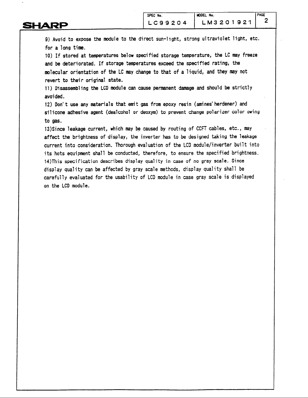
9) Avoid to expose the module to the direct sun-light, strong ultraviolet light, etc.
for a long time.
10) If stored at temperatures below specified storage temperature, the LC may freeze
and be deteriorated. If storage temperatures exceed the specified rating, the
molecular orientation of the LC may change to that of a liquid, and they may not
revert to their original state.
11) Disassembling the LCD module can cause permanent damage and should be strictly
avoided.
12) Don't use any materials that emit gas from epoxy resin (amines'herdener) and
silicone adhesive agent (dealcohol or deoxym) to prevent change polarizer color owing
to gas.
13)Since leakage current, which may ba caused by routing of CCFT cables, etc., may
affect the brightness of display, the inverter has to be designed taking the leakage
current into consideration. Thorough evaluation of the LCD module/inverter built into
its hots equipment shall be conducted, therefore, to ensure the specified brightness.
l4)This specification describes display quality in case of no gray scale. Since
display quality can be affected by gray scale methods, display quality shall be
carefully evaluated for the usability of LCD module in case gray scale is displayed
on
the LCD module.
I
I
SPEC Ho. HODEL Ho.
LC99204
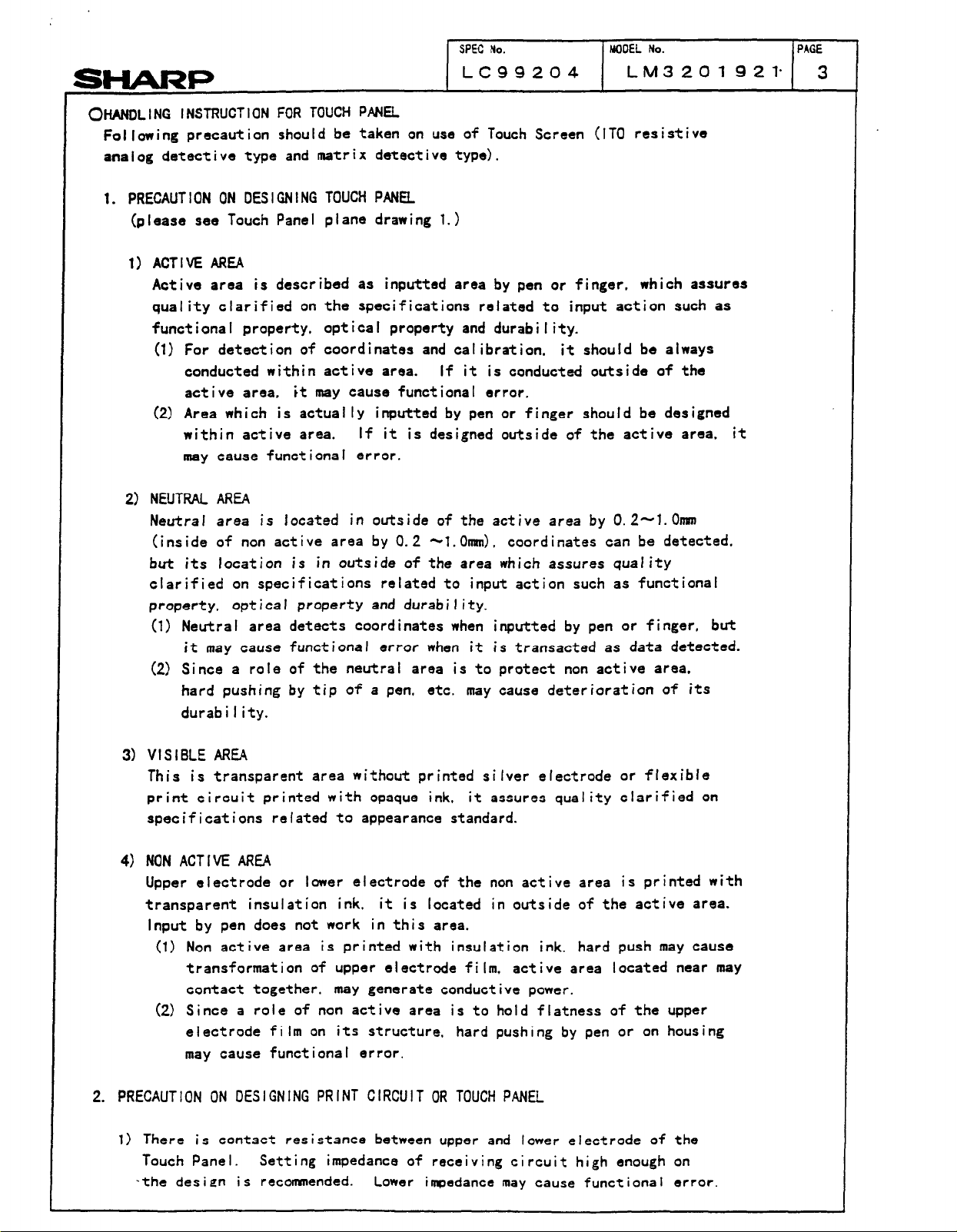
OHANCLING INSTRUCTION FOR TOUCH PANEL
Following precaution should be taken on use of Touch
analog detective type and matrix detective type).
1. PRECAUTION ON DESIGNING TOUCH PANEL
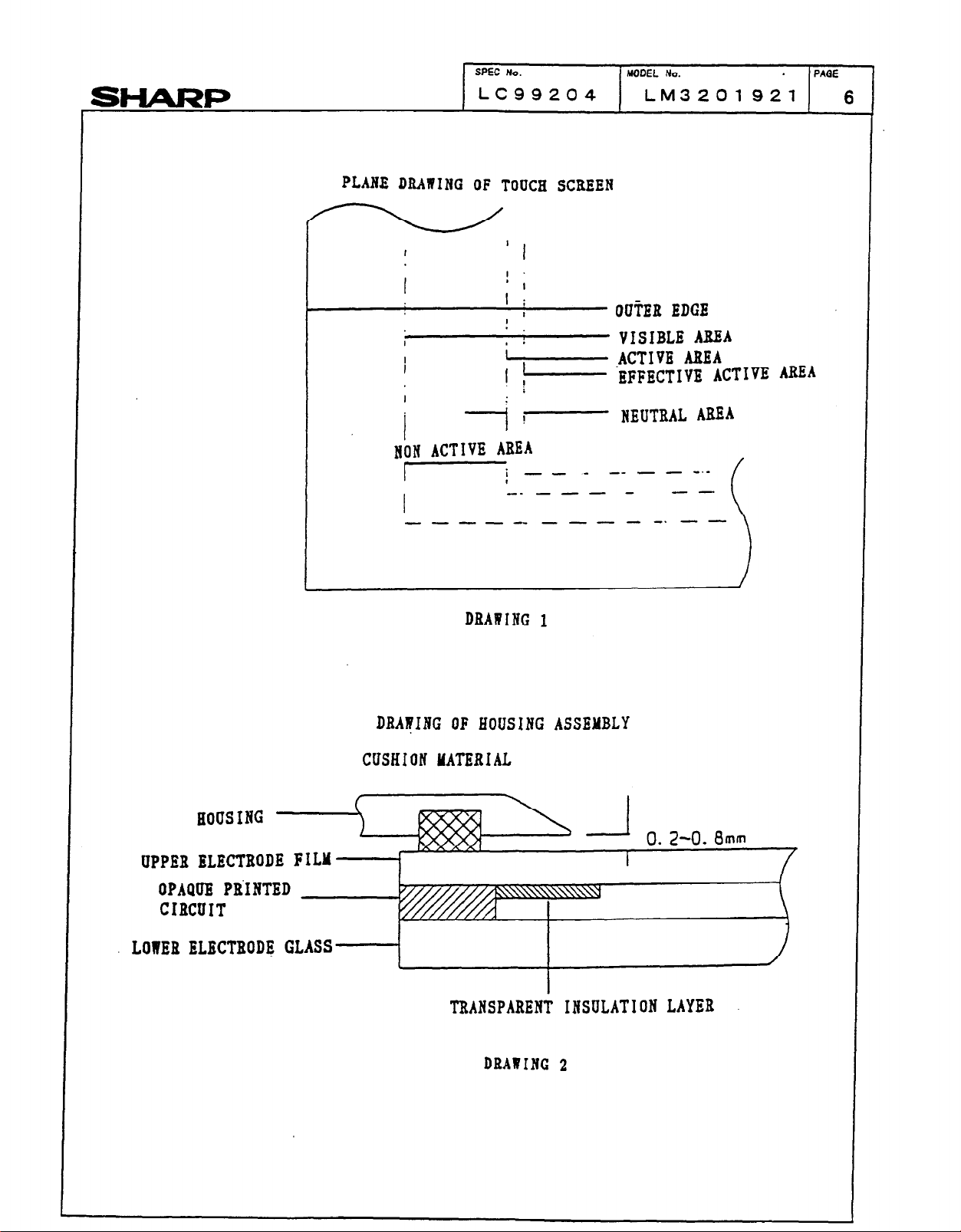
(please see Touch Panel plane drawing 1.)
1) ACTIVE AREA
Active area is described as inputted area by pen or finger, which assures
quality clarified on the specifications related to input action such as
functional property. optical property and durabi I ity.
(1) For detection of coordinates and calibration. it should be always
conducted within active area. If it is conducted outside of the
act i ve area. it may cause functional error.
(2) Area which is actually inputted by pen or finger should be designed
within active area. lf it is designed outside of the active area. it
may cause functional error.
2) NEUTRAL AREA
Neutral area is located in outside of the active area by 0.2-1.011x11
(inside of non active area by 0.2 -~l.Onm~). coordinates can be detected.
but its location is in outside of the area which
clarified on specifications related to input action such as functional
property, opt i ca I property and durab i I i ty.
Neutral area detects coordinates when inputted by pen or finger, but
(1)
it
may cause functional error when it is transacted as data detected.
Si rice a role of the neutral area is to protect non active area.
(2)
hard pushing by tip of a pen, etc. may cause deterioration of its
durab i I i ty.
Screen
assures
LM3201 921.
(IT0 resistive
quality
PAGE
3
3) VIS I
BLE AREA
Thi
S
is transparent area without printed silver electrode or flexible
print circuit printed with opaque ink, it assures quality clarified on
spec if i cat ions
re
la-tad to appearance standard.
4) NON ACTIVE AREA
Upper electrode or lower electrode of the non active area is printed with
transparent insulation ink. it is located in outside of the active area.
Input by pen does not work in this area.
(1) Non active area is printed with insulation ink. hard push may cause
transformation of upper electrode film, active area located near may
contact together.
may generate conductive power.
(2) Since a role of non active area is to hold flatness of the upper
electrode film on its structure. hard pushing by pen or on housing
may cause functional error.
2. PRECAUTION ON DESIGNING PRINT CIRCUIT OR TOUCH PANEL
1) There is contact resistance between upper and
lower electrode
Touch Pane I. Setting impedance of receiving circuit high enough on
-the desien is recommended. Lower irrpedance may
cause
functional
of the
error
SHARP
2) Conduction between upper and lower electrode generates contact
res i stance. Data
contact res i stance become stab I e enough. Otherwise it may cause
functional error.
input
SPEC no.
LC99204
by pen or finger should be started after the
MGDEL No. PAGE
LM320192J
4
3) Touch Pane I picks up noise eas i I y, any measures such as earth. etc
recosxaended. Otherwise it may cause functional error.
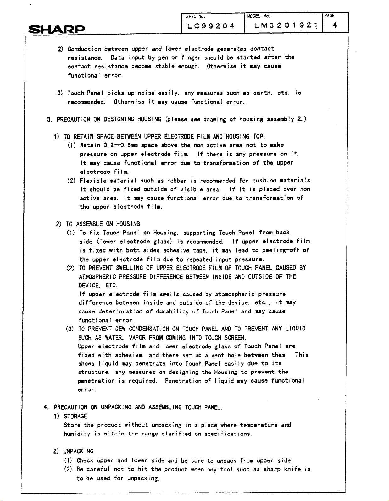
3. PRECAUTION ON DESIGNING HOUSING (please see drawing of housing assemb
11 TO RETAIN SPACE BE-MEN UPPER ELECTRODE FILM AND HOUSING TOP.
(1) Retain 0.2-O. &mu space above the non active area not to make
pressure on upper electrode film. If there is any pressure on
It may cause functional error
electrode f i Im.
(2) Flexible material such as robber is recoaxaended for cushion materials.
It should be fixed outside of visible area.
act i ve area. it may cause functional error due to transformation of
the upper electrode film.
2) TO ASSEMBLE ON HOUSING
(1) To f i x Touch Panel on Hous i ng. supporting Touch Panel from back
side (lower electrode glass) is reconxnended.
is fixed with both sides adhesive tape, it may lead to peeling-off of
the upper electrode film due to repeated input pressure.
(2) TO PREVENT SWELLING OF UPPER ELECTRODE Fl LM OF TOUCH PANEL CAUSED BY
ATMOSPHERIC PRESSURE DIFFERENCE BETWEEN INSIDE AND OUTSIDE OF THE
DEVI CE. ETC.
If
upper electrode film
difference between inside and outside of the device, etc., it may
cause deterioration of durability of Touch Panel and may cause
functional error.
(3) TO PREVENT DEW CONDENSATION ON TOUCH PANEL AND TO PREVENT ANY LICU I D
SUCH AS WATER, VAPOR FROM COMING I NT0 TOUCH SCREEN.
Upper electrode film and lower electrode glass of Touch Panel are
fixed with adhesive. and there set
shows liquid may penetrate into Touch Panel easily due to its
structure. any measures on designing the Housing to prevent the
penetration is required. Penetration of liquid may cause functional
error.
swells caused by atomospheric pressure
due
to transformation of the upper
If it is placed over non
If upper electrode fi Im
up
a vent hole between them.
y
it,
is
2.1
This
4. PRECAUTION ON UNPACKING AND ASSEMBLING TOUCH PANEL.
1) STORAGE
Store the product without unpacking in a place where temperature and
humidity is within the range clarified on spec;fications.
2) UNPACK I NG
(1) Check upper and lower side and be sure to unpack from upper side.
(2) Be careful not to hit the product when any tool such as sharp knife is
to be used for unpacking.
SHARP
(3) Do not hold and pull out flexible tail, otherwise it may cause shut
(4) Any treatment i s
3) HANDLING
(1) Pick up outside of visible area for handling. Do not pick up center
I SPEC No.
LC99204
down of the flexible print circuit.
not
made for glass edge. It may
cause any injury when handled by bare hands. Wear a fingerstall or
glove and handle with extra care.
of the visible
area and flexible tail.
1 MOOEL No. 1 PAGE
LM320192i 5
be
sharp and may
(2) Do not stack
It may cause scratch or transformation.
(3) Wipe out any dirt on the product with dried flexible cloth. If it is
heavy dirt, wipe it out with flexible cloth with some ethyl alcohol.
Upper electrode film and lower electrode glass of Touch Panel are
fixed with adhesive, and
Therefore ethyl alcohol may penetrate into Touch Panel easily from
the edge, so extra care is required. It may cause functional error.
4) PRECAUTION ON ASSEMGLY
(1) Be careful not to generate excess distortion on heat sealed area and
flexible tai I. It may cause functional error.
(2) Be careful not to scratch the product on assemb I y.
5) PRECAUTION ON HANDLING
(1) handle the product within the range of temperature and humidity
clarified on specifications.
(2) Use finger or polyacetal pen attached for input to Touch Panel.
Surface of the Touch Panel is bar-code treated, film surface may be
damaged if inputted
up
the products and do not place anything on the product.
there set up
by
ball-point pen or metal piece.
a vent hole between them.
(3) Do not expose Touch Panel to direct sunlight for long period of time.
Polyester film is used on Touch Panel, exposure to direct sunlight
for long period of time may cause discoloration.
(4) If Chemical stays on the Touch Panel for long period of time, upper
electrode film may be swelled and may cause functional error. If it
is to be used under severer circumstances. another measures for water
protection i s requi red.
5. If any other quest i on may be arised. please fee
I free to contact us.
. SHARP
SPEC No.
LC99204
PLANE DRAlING OF TOUCH SCREEN
MGDEL No. PAGE
LM3201 921
6
I
1
I
i
j ,---j !
N&i ACTIVE AREA
I-; - - - -- - - -.- f
I
------_----.
I .
I
I
I I
t
I
* .
;
!+
-.--A -
OUTER EDGE
-EFFECTIVE ACTIVE AREA
VISIBLE ABEA
ACTIVE AREA
NEUTRAL AREA
--
--
\
)
DRAWING 1
HOUS I NG
UPPER ELECTRODE FILM
OPAQUE PRiNTED
CIRCUIT
LOWER ELECTROD! GLASS--{
DRAYIJG OF HOUSING ASSEMBLY
CUSHION MATERIAL
c
)
TRANSPARENT INSULATION LAYER
DRAWING 2
I
0.2-0.8mm
I
/
L
 Loading...