LPREPARED BY: DATE
APPROVED BY:
DATE
SHARP
LIQUID CRYSTAL DISPLAY GROUP
SHARP CORPORATION
SPEC No. LC99908
FILE No.
ISSU OCT. 1.1999
PAGE 23 Pages
REPRENTATIVE DMSION
Model No.
LM057QCTT03
SPECIFICATION
DEVICE SPECIFICATION for
Passive Matrix LCD Module
ENGINEERING DEPARTMENT
DUTY
LCD DEVELOPMENT
CENTER
DUTY LIQUID CRYSTAL
DISPLAY GROUP
1
q
CUST~MER’S USE ONLY
DATE
BY
PRESENTED _
M.Ise
DEPARTMENT GENERAL
ENGINEERING DEPARTMENT 1
DUTY LCD DEVELOPMENT CENTER
DUTY LIQUID CRYSTAL DISPLAY GROUP
/
MANAGER
RECORDS OF REVISION
SPEC.No.
MODEL No.
LC99908 LM057QCTT03
DOC.
FIRST ISSUE
OCT. 1.1999
IDENT. DATA No.
IATE SPEC REVISED REF. PAGE SUIWARY
REVISED No.
No.
-----._--------..----------.----.---------------.-------------------------------------------------------.------------.--------------
---------------..--.--------.----.---------------.----------------.----------------------------------------~----------.--------------
------______---.____------------.---------------.--------------------------------------------------------------------.--------------
------____-__--..___------------.---------------.----------------.-------------------------------------------------.-.--------------
-----__________.________________________--------.--------------~-----------------------------------------------------.---------~.--.-----_________.____------------.---------------.--------------------------------------------------------------------.-------------.------__------_____------------.---------------.--------------------------------------------------------------------.-------------.-----____-----.____------------.---------------.--------------------------------------------------------------------.--------------.
.-----_-____---.-_______________________--------.--------------------------------------------------------------------.--------------.
-___-_________._____-----------.---------------.----------------.---------------------------------------------------.---------------
-----________-.-____-----------.---------------.--------------------------------------------------------------------.--------------.
-----_________._____-----------.---------------.----------------.---------------------------------------------------.---------------
CHECK
?l
APPROVAL
-_---_______________-----------.---------------.----------------.---------------------------------------------------.--------------
-----________-.-________________________-------.--------------------------------------------------------------------.-------------______________._____-----------.---------------.----------------.-----------------.---------------------------------.--------------
__--__________._____-----------.---------------.----------------.-----------------.---------------------------------.-------------______________._____-----------.---------------.----------------.-----------------.---------------------------------.-------------________________________________________-------.----------------------------------.---------------------------------.-------------.___-_________._____-----------.---------------.----------------.---------------------------------------------------.-------------.___________________-----------.---------------.-------~------------------------------------------------------------.-------------._______________________________________-------.--------------------------------------------------------------------.-------------.--___________._________________________-------.--------------------------------------------------------------------.--------------
---_________________----------.---------------.-___________________-------------------------------________________________________________------.----------------.-------------------------------------
____.___________________________________------.--------------------------------------------------------------------
-----_______-.-_________________________------.-------------------------------------------------------------------- ----------_---.
-----________.-_________________________------.________________________________________---------------------------- .--------_------
________________.__------------
_______,_____---------
_-_-me-
.___---_---____
,_.
SHARP
Precautions
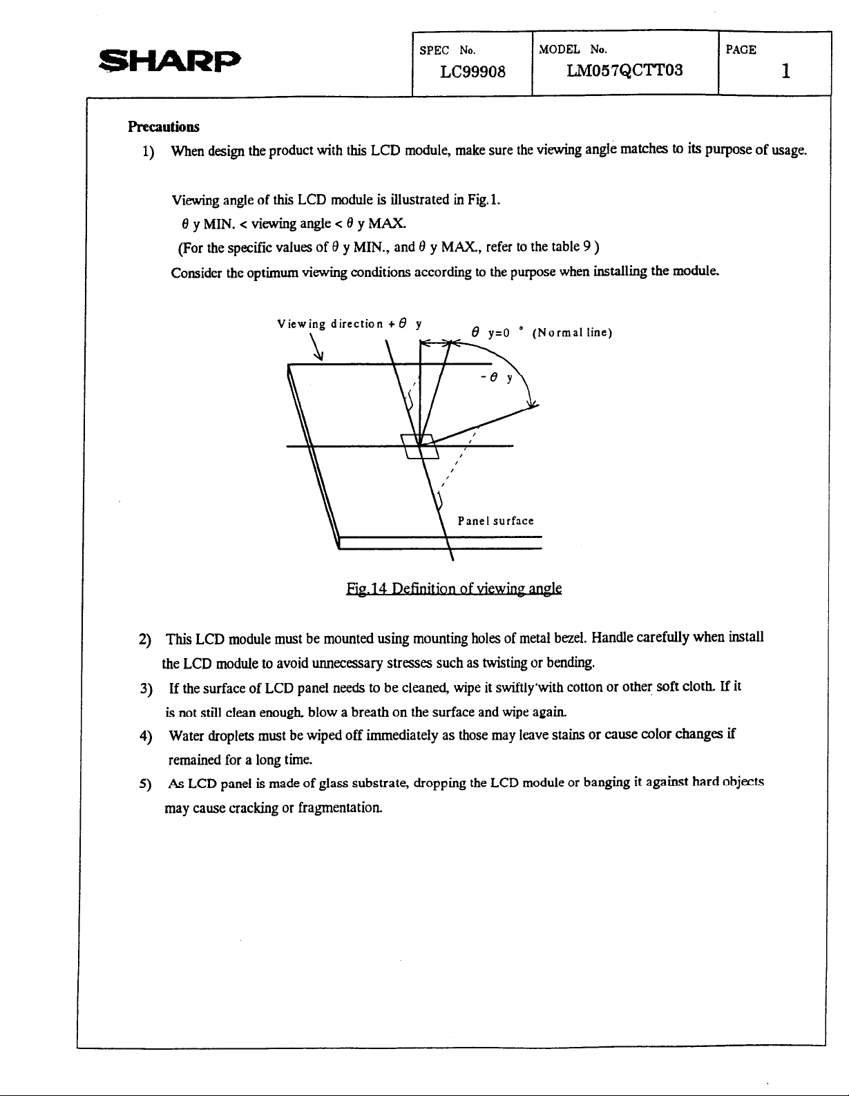
1) When design the product with this LCD module, make sure the viewing angle matches to its purpose of usage.
Viewing angle of this LCD module is illustrated in Fig. 1.
8yMIN.<viewingangle<OyMAX.
(For the specific values of 6 y MIN., and 8 y MAX., refer to the table 9 )
Consider the optimum viewing conditions according to the purpose when installing the module.
SPEC No.
LC99908
MODEL No.
LM057QClT03
I
PAGE
1
I
Viewing direction + 6
Ei~-14 Definttlonofwe~
2) This LCD module must be mounted using mounting holes of metal bezel. Handle carefully when install
the LCD module to avoid unnecessary stresses such as twisting or bending.
3) If the surface of LCD panel needs to be cleaned, wipe it swiftly’with cotton or other soft cloth If it
is not still clean enough, blow a breath on the surface and wipe again
y
Panel surface
. . . .
ormal line)
4) Water droplets must be wiped off immediately as those may leave stains or cause color changes if
remained for a long time.
5)
As LCD panel is made of glass substrate, dropping the LCD module or banging it against hard objects
may cause cracking or fragmentation.
@HARP
6) As CMOS LSIs are equipped in this module, following countermeasures must be taken to avoid
electrostatics charges.
1. Operator
Ware the electrostatic shielded clothes because human body may be statically charged if not ware shielded
clothes.
2. Equipment
I I
SPEC No. MODEL No.
LC99908
LM057QCTT03
I
PAGE
2
There is a possibiiity that the static electricity is charged to the equipment which have a function of
or friction action(ex: conveyer, soldering iron, working table). Earth the equipment through proper
resistance(electrostatic earth: 1 X 10” 9).
3. Floor
Floor is the important part to drain static electricity which is generated by operators or equipment.
There is a possibility that charged static electricity is not properly drained in case of insulating floor.
Set the electrostatic earth(1 X lO”S2).
4. Humidity
Proper humidity helps in reducing the chance of generating electrostatic charges. Humidity should be kept
over 50%RH.
5. Transportation/storage
The storage materials also need to be anti-static treated because there is a possibility that the human body or
storage materials such as containers may be statically charged by friction or peeling.
6. Others
The laminator@rotective film) is attached on the surface of LCD panel to prevent it from scratches or stains.
It should be peeled off slowly using static eliminator.
Static eliminator should also be installed to the work bench to prevent LCD module from static charge.
7) Do not use any materials which emit gas from epoxy resin(hardener for amine) and silicone adhesive
peeling
agent(dealcoho1 or deoxym) to prevent discoloration of polarizer due to gas.
8) The brightness of the LCD module may be affected by the routing of CCFI cables due to leakage to the
chassis through coupling effect. The inverter circuit needs to be designed taking the level of leakage current
into consideration. Thorough evaluation is needed for LCD module and inverter built into its ho& equipment
to ensure specified brightness.
9) Avoid the exposure of the module to the direct sun-light or strong ultraviolet light for a long time.
10) If the LCD module is stored at below specified temperature, the LC material may freeze and be deteriorated
If it is stored at above specified temperature, the molecular orientation of the LC material may change to
Liquid state and it may not revert to its original state. Therefore, the LCD module should always be stored
within specified temperature range.
11) Disassembling the LCD module can cause permanent damage and it should be strictly avoided
@HARP
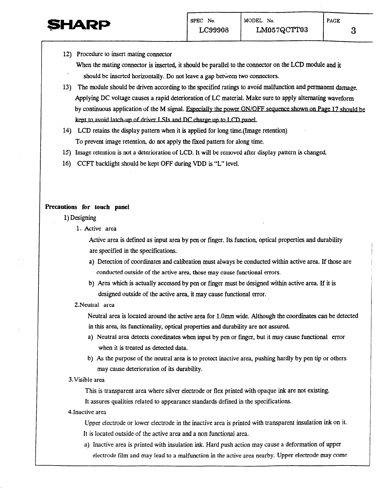
12) Procedure to insert mating connector
SPEC No.
LC99908
MODEL No.
LM057QCTT03
PAGE
3
When the mating connector is inserted, it should be parallel to the connector on the
should be inserted horizontally. Do not leave a gap beh>een two connectors.
13) The module should be driven according to the specified ratings to avoid malfunction and permanent damage.
Applying DC voltage causes a rapid deterioration of LC material. Make sure to apply alternating waveform
by continuous application of the M signal. Espe&&& power ON/OFF sm 17 &n&l&
t to avov DC m
14) LCD retains the display pattern when it is applied for long time.(Image retention)
To prevent image retention. do not apply the flied pattern for along time.
15) Image retention is not a deterioration of LCD. It will be removed after display pattern is changed
16) CCFI’ backlight should be kept OFF during VDD is “L” level.
Precautions for touch panel
1) Designing
1. Active area
Active area is defined as input area by pen or finger. Its function, optical properties and durability
LCD
module and it
are specified in the specifications.
a) Detection of coordinates and calbration must always be conducted within active area. If those are
conducted outside of the active area, those may cause functional errors.
b) Area which is actually accessed by pen or finger must be designed within active area. If it is
designed outside of the active area, it may cause functional error.
2.Neutral area
Neutral area is located around the active area for l.Omm wide. Although the coordinates can be detected
in this area, its functionality, optical properties and durability are not assured.
a) Neutral area detects coordinates when input by pen or finger, but it may cause functional error
when it is treated as detected data.
b) As the purpose of the neutral area is to protect inactive area, pushing hardly by pen tip or others
may cause deterioration of its durability.
3.Visible area
This is transparent area where silver electrode or flex printed with opaque ink are not existing.
It assures qualities related to appearance standards defined in the specifications.
4Jnactive area
Upper electrode or lower electrode in the inactive area is printed with transparent insulation ink on it.
It is located outside of the active area and a non functional area.
a) Inactive area is printed with insulation ink. Hard push action may cause a deformation of upper
electrode film and may lead to a malfunction in the active area nearby. Upper electrode may come
J
@HARP
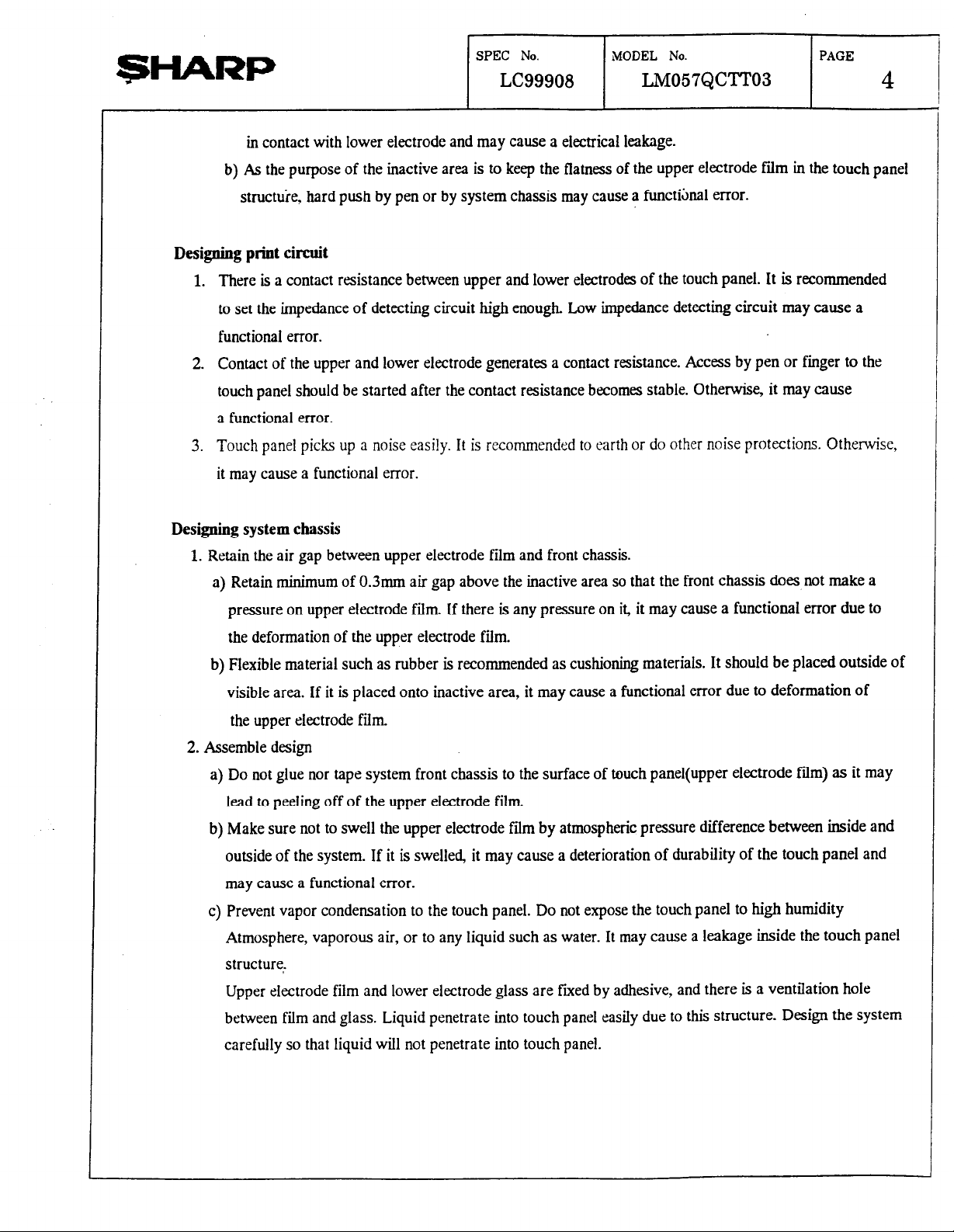
b) As the purpose of the inactive area is to keep the flatness of the upper electrode ftirn in the touch panel
Designing print circuit
1. There is a contact resistance between upper and lower electrodes of the touch panel. It is recommended
to set the impedance of detecting circuit high enough. Low impedance detecting circuit may cause a
functional error.
2. Contact of the upper and lower electrode generates a contact resistance. Access by pen or finger to the
touch panel should be started after the contact resistance becomes stable. Otherwise, it may cause
a functional error.
3. Touch panel picks up a noise easily. It is recommended to earth or do other noise protections. Otherwise,
it may cause a functional error.
r I
SPEC No.
MODEL No. PAGE
LC99908 LM057QCTT03
in contact with lower electrode and may cause a electrical leakage.
structuie. hard push by pen or by system chassis may cause a functi&al error.
I
4
Designing system chassis
1. Retain the air gap between upper electrode film and front chassis.
a) Retain minimum of 0.3mm air gap above the inactive area so that the front chassis does not make a
pressure on upper electrode film. If there is any pressure on it, it may cause a functional error due to
the deformation of the upper electrode film.
b) Flexible material such as rubber is recommended as cushioning materials. It should be placed outside of
visible area. If it is placed onto inactive area, it may cause a functional error due to deformation of
the upper electrode film.
2. Assemble design
a) Do not glue nor tape system front chassis to the surface of touch panel(upper electrode fam) as it may
lead to peeling off of the upper electrode film
b) Make sure not to swell the upper electrode film by atmospheric pressure difference between inside and
outside of the system. If it is swelled, it may cause a deterioration of durability of the touch panel and
may cause a functional error.
c) Prevent vapor condensation to the touch panel. Do not expose the touch panel to high humidity
Atmosphere, vaporous air, or to any liquid such as water. It may cause a leakage inside the touch panel
structure:
Upper electrode film and lower electrode glass are fied by adhesive, and there is a ventilation hole
between film and glass. Liquid penetrate into touch panel easily due to this structure. Design the system
carefully so that liquid will not penetrate into touch panel.
SHARP
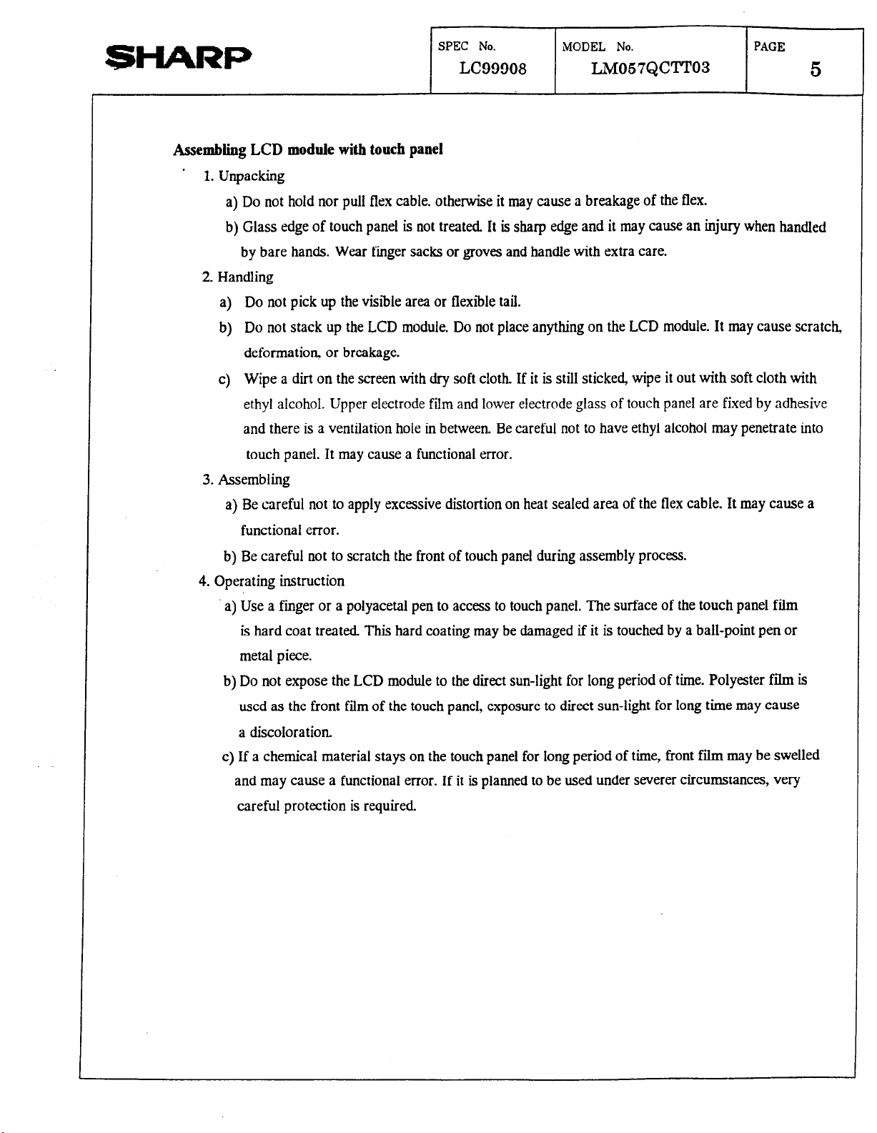
Assembling LCD module with touch panel
* 1. Unpacking
SPEC No.
LC99908
a) Do not hold nor pull flex cable. otherwise it may cause a breakage of the flex.
b) Glass edge of touch pane1 is not treated It is sharp edge and it may cause an injury when handled
by bare hands. Wear finger sacks or groves and handle with extra care.
2. Handling
a) Do not pick up the visible area or flexible tail.
b) Do not stack up the LCD module. Do not place anything on the LCD module. It may cause scratch,
deformation or breakage.
c) Wipe a dirt on the screen with dry soft cloth If it is still sticked, wipe it out with soft cloth with
ethyl alcohol. Upper electrode film and lower electrode glass of touch panel are fixed by adhesive
and there is a ventilation hole in between. Be careful not to have ethyl alcohol may penetrate into
touch panel. It may cause a functional error.
iMODEL No. PAGE
LM057QCTT03
5
3. Assembling
a) Be careful not to apply excessive distortion on heat sealed area of the flex cable. It may cause a
functional error.
b) Be careful not to scratch the front of touch pane1 during assembly process.
4. Operating instruction
a) Use a finger or a polyacetal pen to access to touch panel. The surface of the touch panel film
is hard coat treated. This hard coating may be damaged if it is touched by a ball-point pen or
metal piece.
b) Do not expose the LCD module to the direct sun-light for long period of time. Polyester film is
used as the front film of the touch panel, exposure to direct sun-light for long time may cause
a discoloration
c) If a chemical material stays on the touch panel for long period of time, front film may be swelled
and may cause a functional error. If it is planned to be used under severer circumstances, very
careful protection is required
SHARP
SPEC No. MODEL No. PAGE
LC99908 LM057QCTI'03
6
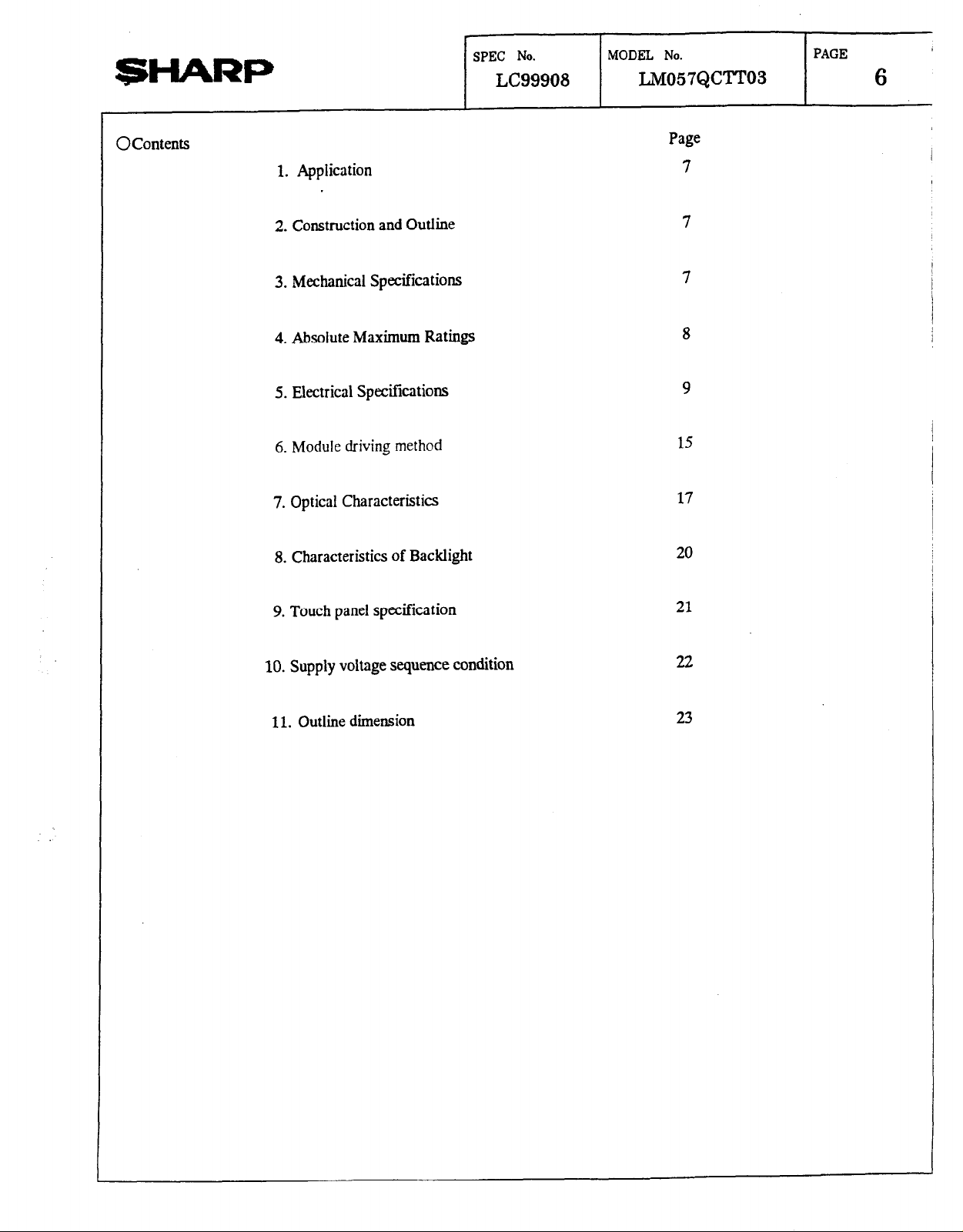
OContents
1. Application
2. Construction and Outline
3. Mechanical Specifications
4. Absolute Maximum Ratings
5. Electrical Specifications
6. Module driving method
7. Optical Characteristics
8. Characteristics of Backlight
Page
7
7
7
15
17
20
9. Touch panel specification
10. Supply voltage sequence condition
11. Outline dimension
21
22
23
 Loading...