

Page 1
q
SERVICE MANUAL
CODE : 00ZLLT1815SME
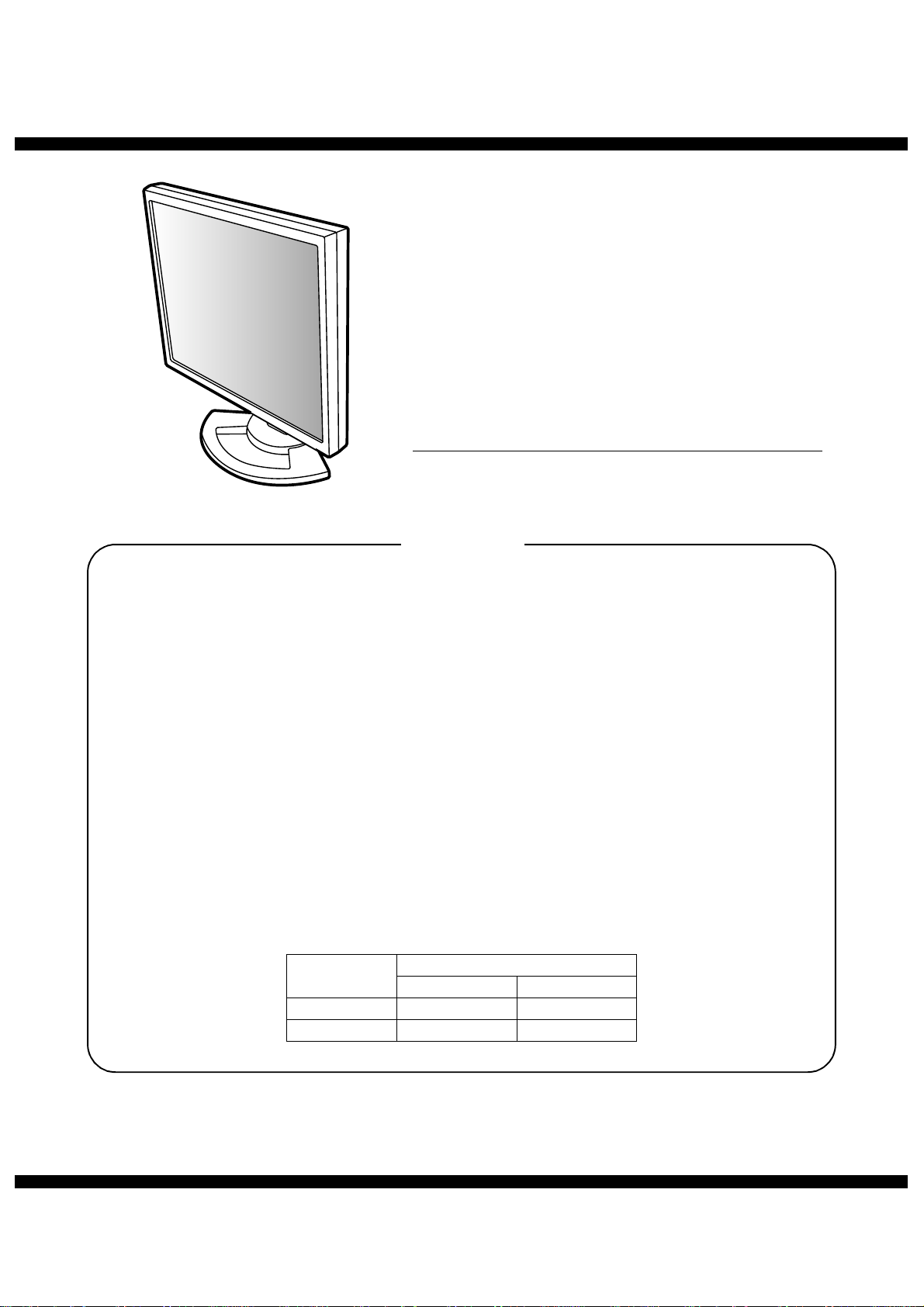
LCD MONITOR
LL-T1815H
MODEL
CONTENTS
CHAPTER 1.
CHAPTER 2.
CHAPTER 3. DISASSEMBLY AND ASSEMBLY. . . . . . . . . . . . . . . . . . . 3 – 1
CHAPTER 4. TROUBLE SHOOTING . . . . . . . . . . . . . . . . . . . . . . . . . . . 4 – 1
CHAPTER 5. WAVE FORM. . . . . . . . . . . . . . . . . . . . . . . . . . . . . . . . . . . 5 – 1
CHAPTER 6. BLOCK DIAGRAM . . . . . . . . . . . . . . . . . . . . . . . . . . . . . . . 6 – 1
CHAPTER 7. CIRCUIT DIAGRAM. . . . . . . . . . . . . . . . . . . . . . . . . . . . . . 7 – 1
OUTLINE OF THE PRODUCT, NOMENCLAT URE AND FUNCTION
CONNECTION, ADJUSTMENT, OPERATION, AND FU NCTIONS
LL-T1815B
. . . 1 – 1
. . . . 2 – 1
CHAPTER 8. PARTS LAYOUT . . . . . . . . . . . . . . . . . . . . . . . . . . . . . . . . 8 – 1
Model Name
LL-T1815H LL-T1815U LL-T1815E
LL-T1815B LL-T1815Y LL-T1815P
Parts mark ed w ith "!" are important for maintaining the safety of the set. Be sure to replace these parts with specified
ones for maintaining the safety and performance of the set.
For North America For others
SHARP CORPORATION
Product Name
This document has been pub lished to be used
for after sales service only.
The contents are subject to change without notice.
Page 2

■■■■SERVICE PRECAUTION
[OVERCURRENT PROTECTION ELEMENT FOR USB OUTPUT OF THE POWER UNIT]
The USB output (5V, connector CN2) of the power unit is provided with an overcurrent protection element (Part Number PTC101) of PTC (positive
characteristics thermister). Its resistance becomes high when heated by an overcurr ent, and shuts down the circuit similarly with a fuse. When it is
cooled down by non-conduction, its resistance returns to a low level and allows a current to flow through the circuit.
If a user erroneously allows an overcurrent to flow through an USB device, the PTC101 cuts off the current. When repaired, it returns to normal. Note
this operation of the PTC 101 in case of an USB error.
LL-T1820-H/B SERVICE PRECAUTION
Page 3

PC-UM10M
CHAPTER 1. OUTLINE OF THE PRODUCT, NOMENCLATURE AND FUNCTION
1. SPECIFICATIONS
■ PRODUCT SPECIFICATIONS
• LCD display
18.1 inches (46 cm measured diagonally)
Advanced-Super-V and Anti Glare Low Reflection TFT LCD module
• Resolution (max.)
SXGA 1280 u 1024 pixels
• Displayable colors (max.)
16.77 million colors (8 bit)
• Brightness (max.)
250cd/m
• Dot pitch
0.2805(H) 0.2805(V) mm
• Contrast ratio
350 : 1
• Angle of visibility
Left-right 160°
• Screen display size
Horizontal 359 mm u Vertical 287.2 mm
• Video signal
Analog: Analog RGB (0.7Vp-p) [75Ω]
Digital: DVI standard based on 1.0
• Sync signal
Separate Sync (TTL level: +/-), Sync on Green,
Composite Sync (TTL level: +/-)
• Expansion compensation
Digital screening
Enlarging VGA/SVGA/XGA etc. with a compensation process.
(no enlarging, based on a fixed aspect ratio, and enlarging to full
screen size.)
• Plug & Play
VESA: DDC2B compatible
• Power management
VESA: based on DPMS
DVI: based on DMPM
• Input signal terminal
Analog: 15 pin mini D-sub(3 rows)
Digital / Analog: 29 pin DVI-I u 2
• Speaker output
1W + 1W
• Audio input terminal
Mini stereo jack
• Headphone terminal
Mini stereo jack
• Height adjustment
Adjustment range: Approx.80 mm
• Screen rotation
Clockwise 0° - 90°
• Screen tilt
Upward approx. 0° - 30°
2
; Up-down 160°
; downward approx. 0° - 5°
• Screen swivel
Approx. 90° from left through right
• Power supply
AC100-240V, 50/60Hz (Use special AC adapter, type NL-A03E of
Sharp Corporation.)
• Temperature of operating environment
5 - 35°C
• Power consumption
51W(With no audio input)
(55W maximum, 5W when in power-saving mode)
• Dimensions (W u D u H)
With long width screen: 395 mm u 213 mm u 427(- 507) mm
With long height screen: 324 mm u 213 mm u 463(- 543) mm
• Weight (excluding AC adapter)
Approx. 8.7 kg, Display area only, approx. 5.5kg
■ DIMENSIONS (Units: mm)
Special AC adapter
Approx. 2.0 m
Approx. W 120 mm u D 60 mm u H 35 mm
Cable(Accesory)
Analog signal cable: Approx. 2.0 m
Audio cable: Approx. 2.0 m
Cable(Option)
Digital signal cable,
NL-C01E(purchased separately):Approx. 2.0 m
Analogue signal cable,
NL-C02E(purchased separately):Approx. 2.0 m
2-input cable,
NL-C03J(purchased separately):Approx. 025 m
LL-T1815 OUTLINE OF THE PRODUCT, NOMENCLATURE AND FUNCTION
1 – 1
Page 4
PC-UM10M
Relevant signal timings (analog)
Display mode
VESA 640 u 480
640 u 400
720 u 400
800 u 600
1024 u 768
1152 u 864
1280 u 960
1280 u 1024
US text 720 u 400
Power
Macintosh
series
Sun Ultra
series
• Recommended resolution is 1280 u 1024.
• All are compliant only with non-interlaced.
• F requencies for P ower Macint osh and the Sun Ultra series ar e reference values. To connect, another adapter (purchased separately)
may be required.
• If the monitor is receiving timing signals that are not compatible, [OUT
OF TIMING] will appear. Follow your computer's instruction manual
to set the timing so that it is compatible with the monitor.
• If the monitor is not receiving any signal (synch signal), [NO SIGNAL]
will appear.
640 u 480
832 u 624
1024 u 768
1152 u 870
1280 u 1024
1024 u 768
1152 u 900
1280 u 1024
Hsync
(kHz)
31.5kHz 60Hz 25.175MHz
37.9kHz 72Hz 31.5MHz
37.5kHz 75Hz 31.5MHz
37.9kHz 85Hz 36.0MHz
37.9kHz 85Hz 31.5MHz
37.9kHz 85Hz 35.5MHz
35.1kHz 56Hz 36.0MHz
37.9kHz 60Hz 40.0MHz
48.1kHz 72Hz 50.0MHz
46.9kHz 75Hz 49.5MHz
53.7kHz 85Hz 56.25MHz
48.4kHz 60Hz 65.0MHz
56.5kHz 70Hz 75.0MHz
60.0kHz 75Hz 78.75MHz
68.7kHz 85Hz 94.5MHz
67.5kHz 75Hz 108.0MHz
60.0kHz 60Hz 108.0MHz
64.0kHz 60Hz 108.0MHz
80.0kHz 75Hz 135.0MHz
31.5kHz 70Hz 28.3MHz
35.0kHz 66.7Hz 30.2MHz
49.7kHz 74.6Hz 57.3MHz
60.2kHz 75Hz 80.0MHz
68.7kHz 75Hz 100.0MHz
64.0kHz 60Hz 108.0MHz
80.0kHz 75Hz 135.0MHz
48.3kHz 60Hz 64.13MHz
53.6kHz 66Hz 70.4MHz
56.6kHz 70Hz 74.25MHz
61.8kHz 66Hz 94.88MHz
71.8kHz 76.2Hz 108.23MHz
71.7kHz 67.2Hz 117.01MHz
81.1kHz 76Hz 134.99MHz
Vsync
(Hz)
Dot frequency
(MHz)
Relevant signal timings (digital)
Display mode
VESA 640 u 480 31.5kHz 60Hz 25.175MH
800 u 600 37.9kHz 60Hz 40.0MHz
1024 u 768 48.4kHz 60Hz 65.0MHz
1152 u 864 67.5kHz 75Hz 108.0MHz
1280 u 960 60.0kHz 60Hz 108.0MHz
1280 u 1024 64.0kHz 60Hz 108.0MHz
US text 720 u 400 31.5kHz 70Hz 28.3MHz
• Recommended resolution is 1280 u 1024.
• All are compliant only with non-interlaced.
• A computer with an output terminal conforming to DVI (DVI-D24 pin
or DVI-I29 pin) and with SXGA output capability can be connected
here.
(Depending on the type of computer to be connected, the display may
not work correctly.)
• If the monitor is receiving timing signals that are not compatible, [OUT
OF TIMING] will appear. Follow your computer's instruction manual
to set the timing so that it is compatible with the monitor.
• If the monitor is not receiving any signal (synch signal), [NO SIGNAL]
will appear.
Hsync
(kHz)
37.9kHz 72Hz 31.5MHz
37.5kHz 75Hz 31.5MHz
48.1kHz 72Hz 50.0MHz
46.9kHz 75Hz 49.5MHz
56.5kHz 70Hz 75.0MHz
60.0kHz 75Hz 78.75MHz
Vsync
(Hz)
Dot frequency
(MHz)
The analog RGB input connector pin
(Mini D-sub connector with 15 pins)
5432
9876
10
15 14 13 12 11
No. Function No. Function
1
Red video signal input
2
Green video signal input
3
Blue video signal input
4
GND
5
GND
6
For red video signal GND
7
For green video signal
GND
8
For blue video signal
GND
1
9
DDC+5V
10
N.C.
11
GND
12
DDC data
13
For Hsync signal input
14
For Vsync signal input
15
DDC clock
LL-T1820-H/B OUTLINE OF THE PRODUCT, NOMENCLATURE AND FUNCTION
1 – 2
Page 5
PC-UM10M
The DVI-I input connector pin
No. Function No. Function
1 TMDS data 2- 16 Hot plug detection
2 TMDS data 2+ 17 TMDS data 03 TMDS data 2/4 shield 18 TMDS data 0+
4 N.C. 19 TMD S data 0/5 shield
5 N.C. 20 N.C.
6 DDC clock 21 N.C.
7 DDC data 22 TMDS clock shield
8 Analogue vertically
23 TMD S clock +
synchronised signal
9 TMD S data 1- 24 TMDS clock 10 TMDS data 1+ C1 Analogue red image signal
11 TMDS data 1/3 shield C2
12 N.C. C3
Analogue green image s igna l
Analogue blue image signal
13 N.C. C4 Analogue horizontally
synchronised signal
14 +5V C5 Analogue GND
15 GND
Power management
The monitor is based on the VESA DPMS*1 and the DVI DMPM*2 standards.
To activate the monitor's Power Management function, both the video
card and the computer must conform to the VESA DPMS standard and
the DVI DMPM standard.
*1 DPMS: Display Power Management Signalling
DPMS mode Sc reen
ON Display on 51W
Power
consumption
H-sync V-sync
Yes Yes
(with no audio
input)
STANDBY Display off 5W No Yes
SUSPEND Yes No
OFF No No
*2 DMPM: Digital Monitor Power Management
DPMS mode Screen Power consumption
ON Display on 51W (with no audio input)
OFF Display off 5W
DDC (Plug & Play)
This monitor supports the VESA DDC (Display Data Channel) standard.
DDC is a signal standard for carrying out Plug & Play functions on the
monitor or PC. It transfers information such as degree of resolution
between the monitor and PC. You can use this function if your PC is
DDC compliant and if it is set so that it can detect the Plug & Play monitor.
There are many varieties of DDC due to the differences between systems. This monitor works with DDC2B.
PRODUCT DESCRIPTION
Front side
7
2 3 4 5 6
1
8
1. INPUT button: To switch between the sign als input term inals. (Input terminal 1 0 Input terminal 2)
2. MENU button: This button is used to pop-up, select and
close the OSD (On Screen Display) Menu.
3. c button: This button is used to select menu options
when the OSD Menu is displayed.
4. e d buttons: When the OSD Menu is displayed:
These button s are used to i ncrease or
decrease the value of a selected option.
When the OSD Menu is not displayed:
These buttons are used to adjust backlight
brightness and speaker volume.
5. Power button
6. Power LED: This LED is lit green when in use and
orange when in power-saving mode.
7. Speakers: Audio entering via the monito r and the
external device connected to the mon itor
can be heard.
8. Headphone terminal: Headp ho n es (c om me rc ia ll y a va ila b le) ca n
be connected here.
9. Audio input terminal: A comp uter’s audio output terminal can be
connected here. The audio ca ble included
should be used.
10. DVI-I input terminal:
(INPUT-2)
The computer’s digital RGB output term inal
or analog RGB ou tput term inal c an be c onnected here.
Separately sold cables are necessa ry for
connection.
For a digital si gnal input: It can be co nnected to a computer with a DVI-compatible
output terminal (DVI-D24 pin or DVI-I29 pin)
and which has SXGA output ability.
Depending on the co mputer to be connected, correct display ma y or may not b e
possible.
11. Analog RGB input
terminal(INPUT-1)
The analog signal c able is connected
here.The analog signal cable included
should be used.
12. Security lock anchor: By connecting a security lock (commercially
available) to the security lock anchor, the
monitor is fixed so that it cannot be transported.
The security slot works in conjunction with
Kensington Micro Saver Security Systems.
13. Power terminal
14. Main power switch
15. Ventilatio n op en i ng s :
Note: Never block the ventilation openings
as this may lead to overheat ing insi de the
monitor and result in malfunction.
Rear side
10 13
9
12
11
15
7
14
15
LL-T1815 OUTLINE OF THE PRODUCT, NOMENCLATURE AND FUNCTION
1 – 3
Page 6
PC-UM10M
HEIGHT ADJUSTMENT, ANGLE ADJUSTMENT,
ROTATION (LONG HEIGHT/WIDTH)
Caution: • Pressure from hands on the LCD panel could cause dam-
age.
• Be careful not to allow your fingers to be pinched.
Height adjustment
Adjust to an easy to view height.
Approx. 80mm
Angle adjustment
Adjust to an easy to view angle.
Approx. 30
Approx. 5
Approx. 45
Rotation (long height/width)
The display can be rotated for a long height or width to suit the displayed content.
• Before rotating, move the display to its uppermost position. If the display is rotated while it is set low, it will contact the stand and could
lead to damage.
• The display can only be rotated through a range of 90°. Applying
excessive force may cause malfunction.
• Do not apply excessive force when the cable is connected.
To set to long height
Gently turn in the clockwise direction (to 90°).
To set to long width
Gently turn in the counterclockwise direction (to 90°).
Approx. 45
Note: The orientation of the display can be changed using Pivot S oft-
ware.
LL-T1820-H/B OUTLINE OF THE PRODUCT, NOMENCLATURE AND FUNCTION
1 – 4
Page 7
PC-UM10M
CHAPTER 2. CONNECTION, ADJUSTMENT, OPERATION, AND FUNCTIONS
1. CONNECTING THE MONITOR AND TURNING THE MONITOR ON AND OFF
Caution: • When connecting, ensure that both the monitor and com-
puter are switched off.
• Be careful not to overly bend the cable or add extension
cords as this could lead to malfunction.
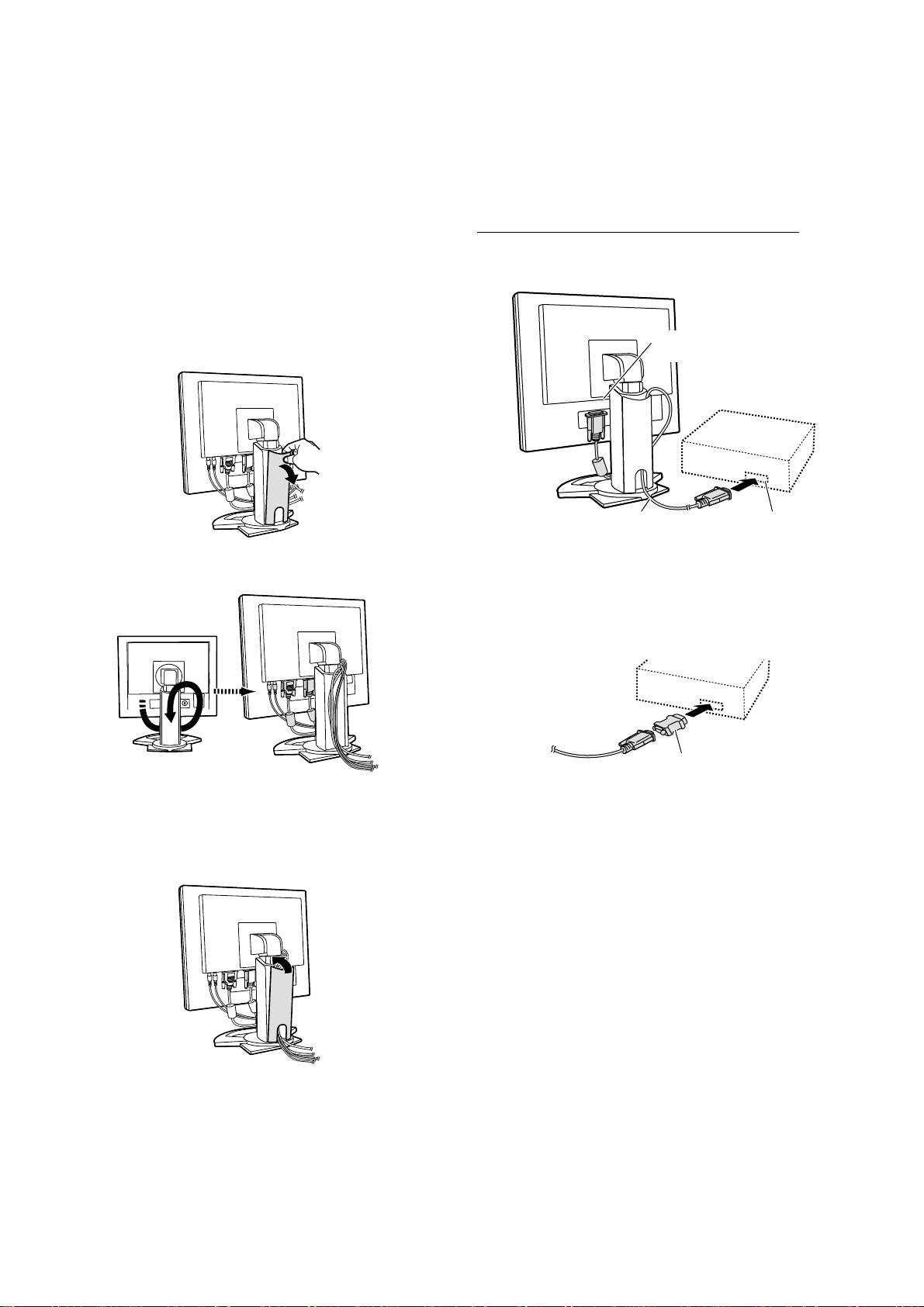
Cable storage
If necessary, excess cable can be housed in the stand.
1. Remove the cover.
Gently pull the top of the cover towards yourself.
2. Run cable along the back of the stand.
Pass cable in front of the stand, and then bring it through the back.
CONNECTING THE MONITOR TO A COMPUTER
Connecting using accessory analog signal cable
Connect the accessory analog signal cable to the analog RGB input terminal of the display, and the analog RGB output terminal of the computer.
Analog RGB input
terminal
Analog signal cable
• Paying attention to connector direction, firmly insert the signal
cable to terminal, and then tighten the screws at both sides.
If connecting to a D-sub 15 pin 2 row Apple P ower Macint osh, attach a
Macintosh conversion adapter (commercially available) to the analog
signal cable.
Analog RGB output
terminal
• If the display is to be ro tated, first house the cab les with the display in the long height position, so there is sufficient length when
the display is turned.
3. Refit the cov e r.
Be careful not to pinch the cable.
• If the cover is hard to refit, do not force it. Check whether cables
are trapped.
Caution: If the display is to be rotated, first house the cable, and then
check while gently turning the display. If it cannot be turned,
rehouse the cable with sufficient slack. (If there is insufficient
cable length, rotation will be impossible. Forcing rotation may
cause cable disconnection.)
Macintosh conversion adapter
LL-T1815 CONNECTION, ADJUSTMENT, OPERATION, AND FUNCTIONS
2 – 1
Page 8
PC-UM10M
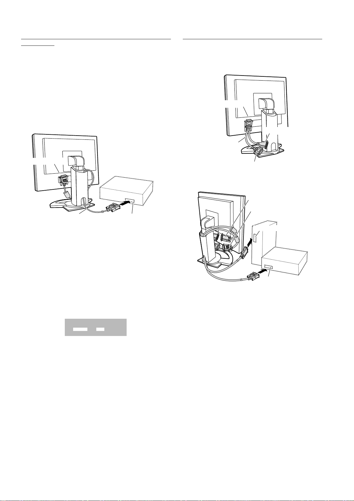
When connecting using separately sold digital or analog
signal cables
The separately sold display cable enables connection between the DVII input terminal on the display and the digital or analog RGB output terminal of the computer.
When connecting to a digital RGB output terminal:
• Use a digital signal cable (model name: NLC01E)
• For digital RGB connection, the monitor has an input for connecting
to a computer with a DVI-compatible output connector (DVI-D 24 pin
or DVI-I 29 pin) and SXGA output capability. (Depending on the type
of computer to be connected, the display may not work correctly.)
When connecting to an analog RGB output terminal:
• Use an analog signal cable (model name: NLC02E).
DVI-I input terminal
Display cable
(purchased separately)
• Paying attention to connector direction, firmly insert the signal
cable to terminal, and then tighten the screws at both sides.
Note: When using digital or analog signal cables, set [INPUT-2] to
[1 LINE].
Set the monitor as follows when establishing a digital connection wit h a
Power Mac using an ADC-DVI ada pter made by Belkin. (Operation has
been checked with the Power Mac G4 M7627J/A)
• Perform settings with the Power Mac power supply off.
1. After connecting the power cord, turn on the monitor’s main power.
2. Press the e button and d button simultaneously, and while doing
this press the POWER button (i.e. turn the power on).
˩˝˟ȁˠ˥ˣ˥˰˝˨
ŊŏőŖŕĮij ŐŇŇ Őŏ
RGB output terminal
When connecting using a separately sold 2-input cable
The separately sold 2-input cable (model name:NLC03J) enables 2 system connection.
1. Connect a 2-input cable (purchased s eparately) to the DVI-I input
Cterminal on the display.
DVI-I input terminal
mini D-sub 15 pin
2-input cable
(purchased
separately)
DVI-D24 pin
2. Connect the analog and digital signal cables ( purchas ed s eparat ely)
to the 2-input cable, then connect to a computer.
Analog signal cable
Digital signal cable
(NL-C01E, purchased separately)
Analog RGB output terminal
Digital RGB output terminal
• Paying attention to connector orientation, firmly insert the signal cable
into the PC, and then tighten the screws at both sides.
Notes:
• When using a 2-input cable, set [INPUT-2] to [2LINES].
• The monitor connected to the mini D-sub connector of the 2-input
cable may not be automatically recognized and setup under Plug &
Play. Perform storage of setup information manually.
3. Set the input terminal to which the Belkin ADC-DVI adapter is connected to ON.
Use the SELECT button to select [INPUT1] or [INPUT2], and use
the e d buttons to select [ON] and [OFF].
• Do not set to [ON] if you are not using a Belkin ADC-DVI adapter,
as this may result in incorrect display.
4. Press the power button, and turn off the monitor power.
This completes setting.
LL-T1820-H/B CONNECTION, ADJUSTMENT, OPERATION, AND FUNCTIONS
2 – 2
Page 9
PC-UM10M
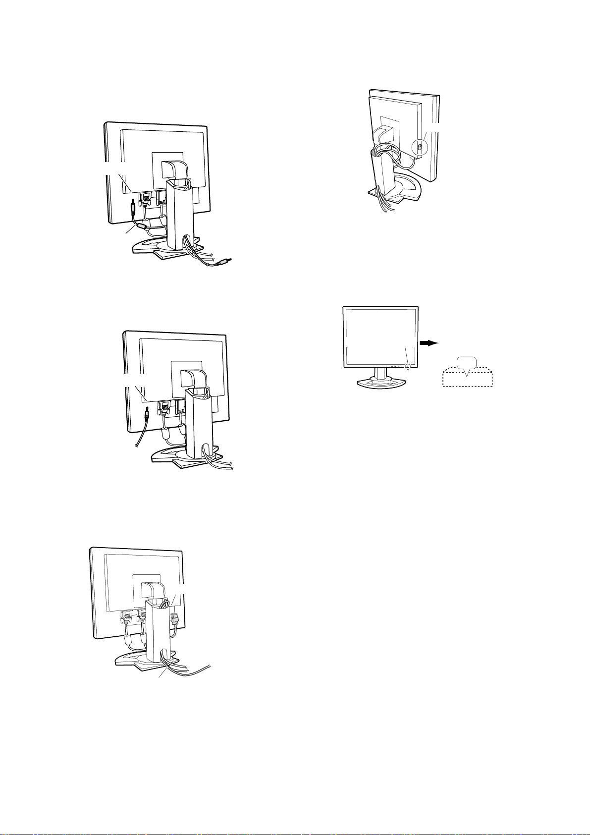
Connect the accessory audio cable
When the accessory audio cable is connected to the audio output terminal of the computer, the sound of the connected computer is output
from the display speakers. You can also use the headphone jack of the
display.
Audio input terminal
Audio cable
To audio output
terminal
CONNECTION OF HEADPHONES
(COMMERCIALLY AVAILABLE)
Headphones (commercially available) can be connected.
TURNING THE POWER ON
1. Turn on the main power of the monitor.
Main power switch
• When switching the main power switch on and off, always wait
for an interval of at least 5 seconds. Rapid switching may result
in malfunction.
2. Press the monitor’s POWER button.
The power LED will light up orange.
3. Turn on the computer.
Press power button
Turn on the computer
power supply.
Headphone terminal
Headphones
Notes:
• When the headphones are connected, no sound c an be heard from
the monitor speakers.
CONNECTING THE MONITOR TO A POWER SOURCE
Power terminal
ON
When a signal is input from the computer, the power LED lights up
green, and the screen is displayed (After power is turned on, it may
take a little time until the screen is displayed.)
• If the input terminal to which the computer is connected has not
been selected, the screen will not be displayed. If necessary,
perform input terminal switching. (right column)
Notes: (when using an analog signal)
• I f using the monitor for the first time or after having c hanged the sys tem settings during use, perform an automatic screen adjustment.
• When connecting to a notebook, if the notebook computer’s screen is
set so that it is displaying at the same time, the MS-DOS screen m ay
not be able to display properly. In this case, change the settings so
that only the monitor is displaying.
Power cord
AC outlet
LL-T1815 CONNECTION, ADJUSTMENT, OPERATION, AND FUNCTIONS
2 – 3
Page 10
PC-UM10M
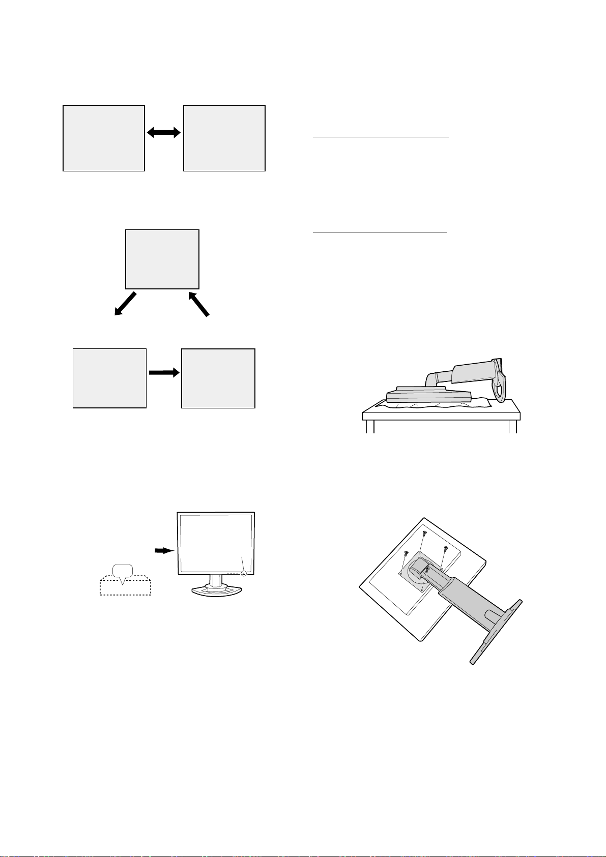
CHANGING BETWEEN INPUT TERMINALS
Use the INPUT button to switch between signal input terminals.
Select [INPUT-1] Select [INPUT-2]
INPUT-1
< >
The input signal type (ANALOG/DIGITAL) is displayed within angle
brackets < >.
When using a 2-input cable
Select [INPUT-2]
(analog)
INPUT
Select [INPUT-1]
INPUT-1
INPUT-2
< >
INPUTINPUT
Select [INPUT-2]
(degital)
2. INST RUCTIONS FOR ATTACHING A VESA COMPLIANT ARM
An arm or stand based on the VESA st andard (com mercially available)
can be attached to the monitor.
Procurement of the arm or stand is at the customer’s discretion.
Arms or stands able to be used
Attachments must satisfy the following.
• Compatible with the VESA standard
• Have a gap of 100 mm x 100 mm between the screw holes on the
section to be attached
• Not be likely to fall off or break off after being attached to the monitor.
How to attach the arm or stand
• Be careful not to overly bend the cable or add extension cords as this
could lead to malfunction.
• While following these instructions, please also refer to the installation
instructions in the operation manual included with the arm or stand.
1. Remove the cable.
2. Spread out a soft cloth on a suitable horizontal surface.
3. Being careful not to damage the monitor, gently lay the monitor on it
display-side down.
INPUT 2-A
<ANALOG>
Note:
• When there is no input signal, [NO SIGNAL] is displayed.
INPUT
INPUT 2-D
<DIGITAL>
TURNING THE POWER OFF
1. Turn the computer off.
2. Press the monitor’s POWER button.
The Power LED will disappear.
Turn the computer off
OFF
If the monitor will not be used for a long time, turn off the main power
switch of the monitor, and remove the power plug from the outlet.
Press power button
Caution: Securely grasp both the display and stand, and gently tip over.
When the monitor is inclined, the stand may suddenly pop out
and cause injury.
4. Remove the four screws and then remove the stand from the monitor.
Notes: • The stand is specially made for use with this monitor. Once
having removed the stand, never attempt to attach it to
another device.
• Once having removed the screws, store them together with
the stand and if the stand is ever re-attached be sure to use
the original screws. Using different screws could lead to a
malfunction.
Caution: Do not disassemble the stand. Parts may spring out and cause
injury.
LL-T1820-H/B CONNECTION, ADJUSTMENT, OPERATION, AND FUNCTIONS
2 – 4
Page 11
PC-UM10M
5. Attach the arm to the monitor with the four screws.
Note: The screws used to attach the arm should be M4 screws with a
length of 6 mm ~ 8 mm protruding from the surface to be
attached. Using different screws could lead to malfunction or may
lead to the monitor falling off,internal damaged,personal injury.
6 - 8mm
Screw used to attach arm
Arm
Part of monitor to which arm is attached
11.Click on [Install].
Installation will begin.
12.When the message indicating installation is finished is displayed,
click [Next].
13.Click on [Finish].
14.Click on [Yes] and restart the computer.
For Macintosh
1. Quit all applications being used.
2. Load the accessory CD-ROM into the CD-ROM drive of the computer.
3. Open the CD-ROM.
4. Double click on the [Pivot] folder.
5. Select the desired language.
6. Double click on [Install MacPortrait].
7. Drag the [MacPortrait Install] icon onto the desired disk.
Installation will begin.
8. When the message indicating installation is finished is displayed,
click on [Restart].
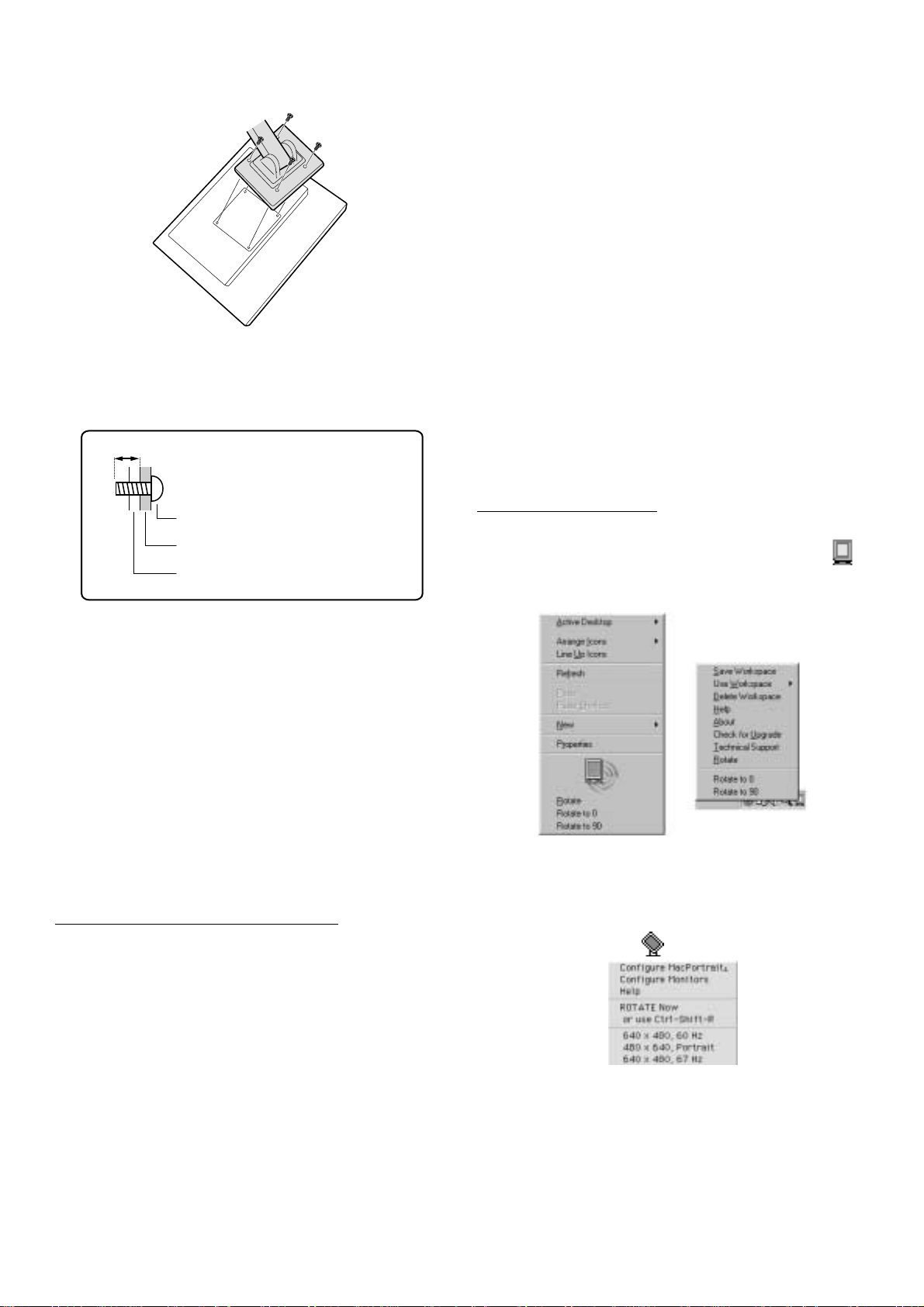
Switching display direction
For Windows
1. Click the right mouse button or click the left mouse button on at
the lower right of the screen.
2. Select [Rotate], [Rotate to 0] or [Rotate to 90].
INFORMATION ABOUT THE PIVOT SOFTWARE
(LONG HEIGHT/WIDTH DISPLAY)
When rotating the display, change the display orientation using Pivot
Software.
Compatible operating systems (OS) for the Pivot Software (trial version)
that comes with the monitor:
Windows 98/2000/Me/XP
Macintosh OS 8.x - 9.1
• Depending on the graphics accelerator, it m ay be impossible to use
Pivot Software, even with a compatible OS.
For production information and inquiries regarding Pivot Software:
Portrait Displays, Inc.
(http://www.portrait.com)
Installation of Pivot Software (trial version)
For Windows
1. Quit all applications being used.
2. Load the accessory CD-ROM into the CD-RO M drive of the computer.
3. Open the [My computer] CD-ROM.
4. Double click on the [Pivot] folder.
5. Double click on [SETUP.exe].
6. Click [Next].
7. Choose [I accept the tems in the License Agreement].
8. Click [Next].
9. Input your Customer information [User Name] and [Organization].
10.Click [Next].
Rotate : The display direction switches.
Rotate to 0: The display direction is switched to long width.
Rotate to 90:The display direction is switched to long height.
For Macintosh
Choose [ROTATE Now] from at the lower right of the screen.
Each time [ROTATE Now] is selected, the display direction switches.
Notes:
• Rotation of the display to match the display direction is done manually.
• The display direction on the OSD menu is switched using [OSD
PIVOT] on the [MODE SELECT-2] menu.
LL-T1815 CONNECTION, ADJUSTMENT, OPERATION, AND FUNCTIONS
2 – 5
Page 12

2. ADJUSTMENT
2-1. ADJUSTMENT METHOD
1) All reset of the adjustment values
While pressing + , turn on the power.
2) Reset of the ADJUSTMENT menu
MENU
3) Adjustment lock and lock release
While pressing , turn on the power.
ȁ
Valid even when there is no input signal.
ȁ
When the above procedure is executed, key lock/release is changed over.
ȁ
When key lock is set, the black display is shown and "ADJUSTMENT LOCKED" is displayed for about 3 sec.
ȁ
When key release is set, the black display is shown and "ADJUSTMENT UNLOCKED" is displayed for about 3 sec.
ȁ
When key lock is set, all the keys except for the power key are disabled.
4) Backlight brightness adjustment
Adjust with and . (Select BRIGHT.)
5) Speaker sound volume adjustment
Adjust with and . (Select VOLUME.)
6) Display adjustment
MENU
ADJUSTMENT AUTO
(Analog only)
GAIN
MENU
CONTROL
(Analog only)
COLOR
MENU
CONTROL
MENU
MENU
simultaneously.Press +
CLOCK
PHASE
H-POS
V-POS
AUTO
BLACK LEVEL
CONTRAST
COLOR MODE (sRGB, STD, VIVID)
(Adjust with .)and
(Adjust with .)
(Adjust with .)
(Adjust with .)
(Adjust with .)
(Adjust with .)
and
and
and
and
and
(Adjust with .)
PC-UM10M
and
MENU
MODE SELECT-1
MENU
MODE SELECT-2 OSD
MENU
ၭ
WHITE BALANCE WHITE BALANCE
GAMMA
INFORMATION
(Adjust with .)
MENU
OFF TIMER
INPUT-2
LANGUAGE
EXPAND
SCALING
400 LINES
(Analog only)
(Adjust with .)
(Adjust with .)
(Adjust with .)
(Adjust with .)
OSD H-POSITION
MENU
COOL STD
MENU
and
(Display)
MENU
and
(Adjust with .)
OSD V-POSITION
OSD PIVOT
(Select with .)
MENU
and
and
and
WARM USER
(Adjust with .)
and
(When ON, Adjust with .)and
and
(Adjust with .)
(Adjust with .)
(Adjust with .)
R-CONTRAST
G-CONTRAST
B-CONTRAST
and
(Adjust with .)
(Adjust with .)
(Adjust with .)
and
and
and
and
and
LL-T1820-H/B CONNECTION, ADJUSTMENT, OPERATION, AND FUNCTIONS
2 – 6
Page 13

PC-UM10M
7) Version display
While pressing + , turn on the power.
MENU
VERSION XX
2002. 05. 31
CHECKSUM XXXX
n
Valid even when there is no input signal.
n
The version , the date, and check sum are displayed.
n
When is pressed, the version display disappears.
MENU
n
All the keys except for and the power key are disabled.
n
The version display keeps ON until or the power key is
MENU
MENU
pressed.
8) Set/reset of usage time
While pressing + + , turn on the
INPUT
power.
[Range of adjustment values]
Range of adjustment Initial value
× 10000
0 -6 0
× 1000 0 - 9
× 100 0 - 9
× 10 0 - 9
× 10 - 9
* The maximum set value is 65535.
9) Diagnostic (Self test)
While pressing + , turn on the power.
n
When the diagnostic is executed, no menu is shown.
n
When the diagnosti c is exe c ute d, th e d ispla y sh ow s Red → Green → Blue
→ Yellow → Purple → Light Blue → White → Black repeatedly.
n
When the diagnostic is executed, all the keys exce pt for the po w er key are
disabled.
n
Turn off the power to terminate the diagnostic.
10) Informati on displa y
While pressing + , turn on the power.
INFORMATION
0
0
0
0
SET/RESET USAGE TIME
Press
ȼ
USAGE TIME
MANUAL
ȿ10000
ȿ1000
ȿ100
ȿ10
ȿ1
n
Valid even when there is no input signal.
n
While the top display of usage time setup is display, +
RESET
0
0
1
2
3
to enter the setup menu of usage time.
n
When is pressed with the cursor on MANUAL, the cursor is
shifted to RESET, the messag e of "RESET USAGE TIME" is displayed on
the black background and the usage time is reset to zero. Then the setup
menu of usage time is displayed again. (The cursor is on MANUAL.)
n
Press , and the cursor (the selected item) is shifted down.
n
When the cursor is on X10000, X1000, X100, X10, or X1, the value on
each digit of usage time can be changed with + .
n
When is pressed in the top display or in the setup menu of
MENU
usage time, the display disappears.
MODEL : LL-T1815-H
SERIAL No. : 2A001234
USAGE TIME : 00123 H
OK <MENU>
n
Valid even when there is no input signal.
n
The model name, the serial No., and the usage time are displayed.
n
When is pressed, the display disappears.
MENU
11) MAC DIGITAL setup
While pressing + , turn on the power.
MAC DIGITAL
INPUT-2 OFF ON
n
Valid even when there is no input signal.
n
When is pressed, the MAC DIGITAL mode is turned off, and
the machine performs normal DVH operations.
n
When is pressed, the MAC DIGITAL mode is turned on, and
the machine performs with digital fixed. To display digital signals with MAC,
it is set to ON. When set to ON, the ma chine performs with digital fixed
even when another than MAC is used.
n
n
The initial setup is OFF.
is pressed, the MAC DIGITAL setup menu disappears.
MENU
12) GAMMA setup
While pressing + + , turn on the
MENU
power.
GAMMA 10BIT OFF ON
n
When is pressed, the machine enters the 8bit mode.
LL-T1815 CONNECTION, ADJUSTMENT, OPERATION, AND FUNCTIONS
2 – 7
Page 14

2-2. ADJUSTMENT ITEM LIST
BUTTON ITEM ADJUSTMENT DESCRIPTION
MENU MENU 1:
MENU 1
4
MENU 2
4
MENU 3
4
MENU 4
4
MENU 5
4
MENU END
c Select the item
e d 0~31 Adjusting the backlight
POWER ON, OFF
ADJUSTMENT
MENU 2:
GAIN CONTROL
MENU 3:
COLOR CONTROL
MENU 4:
MODE SELECT-1
MENU 5:
MODE SELECT-2
MANUAL CLOCK 0~255 CLOCK: The figure below demonstrates how to adjust so that verti-
PHASE 0~31 PHASE: Th e f igure below demon s t rat es how to adjust so th at hori-
H-POS 0~ H-POS (h orizontal position ing) and
V-POS 0~
AUTO Automatic screen adjustment
MANUAL BLACK
AUTO GAIN CONTROL Menu
COLOR MODE sRGB, STD, VIVID STD: Displays image with the color tone results from original
WHITE BA LANCE COOL • STD • WARM
GAMMA -10~10 Adj ust s o t hat da rk a nd bri gh t i mag es a re e asy t o s ee. I f th e sc re en is
IINFORMATION
OFF TIMER ON(1 - 23 hours) • OFF Power is auto m atically shut off wh en the set time elapses .
INPUT-2 1LINE • 2LINES
LEVEL
CON-
TRAST
0~100 BLACK LEVEL: Total screen brightness can be adjusted while
0~100 CONTRAST:While watching the color pattern, adjustments can be
(5 levels),
USER R • G • B:
0~100
V-POS (vertical positioning)
AUTO: Every menu option is automatically adjusted using the
sRGB: sRGB is international standard of color representation speci-
VIVID: Displays an image with dy namic and VIVID prim ary colors.
WHITE BALAN C E Menu
USER
dark and hard to see, increase the numerical value. If it is bright and
hard to see, lower the numerical value . ( e d buttons)
A model name (MODEL), a s erial no. (S/N), and u sage time
(USAGE TIME) of the display can be checked.
Set [1 LINE] when connecting digital or analog signal cables to a
DVI-I input terminal (INPUT-2) on the display.
cal flicker noise is n ot em it t ed. (e d buttons)
zontal flicker nois e is not emitted. (e d buttons)
To center the screen image within the boundaries of the screen,
adjust the left-right (H-POS) values and the up-down (V-POS ) values. (e d buttons)
Options in the ADJUSTMEN T M enu can be ad justed auto m at ically
(CLOCK, PHASE, H -POS V-POS).
watching the color pattern. (e d buttons)
made so that all graduations appear. (e d buttons )
Auto Gain Control function.
scheme of liquid crystal panel.
fied by IEC (International Electrotechnical Commission).
Color conversion is made in taking account of liquid crystals
characteristics and re pre sents colo r ton e c lose to it o rigi nal
image.
COOL : Colo r to ne bluer than standa rd
• : Color tone slightly bluer than standard
STD : Color tone standard setting
• : Color tone slightly redder than standard
WARM : Color tone redder than standard
R-CONTRAST : e button for blue-green
G-CONTRAST : e button for purple
B-CONTRAST : e button for yellow
d button for red
d button for green
d button for blue
Set [2LINES] when connecting a 2-input cable.
OSD H-POSITION OSD H-POSITION (OSD horizontal position)
OSD V-POSITIO N OSD V-POSI T IO N (OSD vertical posit ion)
OSD PIVOT OFF(landscape)
LANGUAGE 7 countrys
EXPAND OFF • CN1 • CN2 Fo r display modes of less than 1280 X 1024 pixels, the display can
SCALING 0~4 SCALING (Level of scaling)
400 LINES 640 • 720 400 LINES (degree of resolu t ion)
• ON(portrait )
DEUTSCH, ENGLISH,
ESPANOL, FRANCAIS,
ITALIANO, NETHE RLAND, SVENSKA
The position of the OSD display can be moved to the left and right.
(e d buttons)
The position of the OSD display can be m ov ed up and down.
(e d buttons)
The orientation of the OSD display can be changed.
LANGUAGE
Messages disp layed on the scre en and OSD M enu contents ca n
be changed to the fo llowing languages .
Dutch, English, French, German, Spanish, Italian, Sw edish.
be expanded if desired.
The sharpness of th e image can be adjus te d. (e dbuttons)
You can specify the horizontal resolution of a 400-line screen
when using US text, etc.(e d buttons)
640: 640 u 400 dot mode
720: 720 u 400 dot mode (US text etc.)
PC-UM10M
LL-T1820-H/B CONNECTION, ADJUSTMENT, OPERATION, AND FUNCTIONS
2 – 8
Page 15

PC-UM10M
CHAPTER 3. DISASSEMBLY AND ASSEMBLY
1. Separating the display from the stand
1) Remove the four screws A and remove the display 1 from the stand 2.
2. Display
1) Remove the seven screws B and remove the rear cabinet 3.
2) Remove the seven screws C and remove the PWB shield 4.
3) Remove the harnesses D, F. Remove the three screws E and remove the
*** PWB 5.
4) Remove the harnesses G
PWB 6.
5) Remove the harness J. Remove the five screws K and remove the power
supply PWB 7.
6) Remove the eight screws L and remove the angle 8 from the LCD unit 9.
7) Remove the front cabinet F.
8) Remove the seven harnesses N. Remove the three screws O and remove
the inverter PWB G.
9) Remove the six screws P
LCD unit K.
, H. Remove the 18 screws and remove the main
, H, Q. Remove the angles H, I, J from the
A
1
A
A
2
8
H
6
D
I
I
F
5
4
C
I
E
I
L
G
L
K
9
3
L
C
B
C
I
B
C
C
B
C
K
J
K
12
P
7
10
N
15
11
B
B
O
N
13
O
LL-T1815 DISASSEMBLY AND ASSEMBLY
3 – 1
O
N
14
Q
R
Page 16

3. Stand
1) Remove the five screws A and separate the *** 1 from the base 2.
2) Remove the cover 3.
3) Remove the six screws B and remove the *** 4.
4) Remove one screw C and remove the cover 5.
5) Remove the two screws D and remove the *** 6.
6) Remove the two screws E and remove the *** 7.
7) Pull the *** 9 out of the *** 8.
8) Remove the two screws F and remove the *** F.
9) Remove one screw G and remove the *** G.
10) Remove the three screws H and remove the *** H.
11) Remove the 17 screws and remove the *** I, *** J and *** K.
PC-UM10M
1
2
A
A
12
15
H
9
H
11
G
10
F
4
H
8
5
C
I
14
I
13
I
B
3
D
D
7
B
E
6
LL-T1820-H/B DISASSEMBLY AND ASSEMBLY
3 – 2
Page 17

PC-UM10M
CHAPTER 4. TROUBLE SHOOTING
First of all, check that all the following accessory cables are properly connected.
Also check that the video mode setup of your PC is set to the signal timing conforming to this machine.
Accessory cables
• Exclusive-use AC adapter
• Exclusive-use analog signal cables (RGB cable, DVI-A cable)
• Exclusive-use digital signal cable (DVI-D cable)
THE DISPLAY DOES NOT WORK. (ANALOG RGB)
When the power button is pressed, does the LED
light up?
4 (Yes)
When the RGB cable is disconnected, does the
LED turn from Green to Orange?
4 (Yes)
When the RGB cable is connected again, does the
LED keep Green?
(Without changing from Green to Orange)
4 (Yes)
Does the B/ L light up? (∗ Light leaks from clearance of lead wires on the sheet metal side. )
4 (Yes)
Does the display work properly in each video
mode?
4 (Yes)
There is no abnormality.
3 (No) Execute 1.
3 (No) Execute 1.
3 (No) Execute 2.
3 (No) Execute 3.
3 (No) Execute 4.
1
4
Is 5V (Main PWB LD69) outputted? 3 (No) Check IC28 and its peripheral circuits.
4 (Yes)
Is 5V (Main PWB LD69) outputted? 3 (No) Execute 2.
4 (Yes)
Do Q8 (1 pin) and R196 supply an output? (4.5V) 3 (No) Execute 2.
4 (Yes)
CN5 (2 pin) supply on output? (2.0V) 3 (No) Check Q8 and its peripheral circuits.
Does FB9
Do Q7 (1 pin) and R185 supply an output? (4.5V) 3 (No) Execute 2.
Does FB9
Check connection of the SW cable and the SW
PWB.
•
4 (Yes)
4 (Yes)
CN5 (2 pin) supply on output? (2.0V) 3 (No) Check Q7 and its peripheral circuits.
•
4 (Yes)
LL-T1815 TROUBLE SHOOTING
4 – 1
Page 18

2
4
Is the input signal port connected to the analog signal cable?
4 (Yes)
Is DC+12V outputted from CN7 3PIN - 9PIN? 3 (No) Check the power unit.
4 (Yes)
Is LD60 at DC+5V?
4 (Yes)
Is LD64 at DC+3.3V?
4 (Yes)
Is LD65 at DC+2.5V?
4 (Yes)
Is the voltage across fuse F1 at DC+12.0V?
4 (Yes)
Is the R156 side of C144 at HIGH level (DC+5V)? 3 (No) Check the RESET circuit in the peripheral of IC17.
4 (Yes)
Is the FB15 level varied by ON/OFF of SW in the
front?
4 (Yes)
Is the Q6 output (connected to R157) change d to
HIGH level after turning on the main SW and then
to LOW level (DC+0V)?
4 (Yes)
Is 21PIN of IC16 oscillating?
4 (Yes)
Is the pin on the C113 side of X1 oscillating?
4 (Yes)
Are the signal waveforms of LD11 and LD12 (LD5,
LD6) normal?
4 (Yes)
Is the signal waveform of LD14 (LD15) normal? 3 (No) Check IC2 peripheral circuits.
4 (Yes)
Are the signal waveforms of LD18 and LD19 normal?
4 (Yes)
Are the signal waveforms of LD22 and LD23 normal?
4 (Yes)
Are the signal waveforms of LD20 and LD21 normal?
(Yes)
3 (No)
3 (No)
3 (No)
3 (No)
3 (No)
3 (No)
3 (No)
3 (No)
3 (No)
3 (No)
3 (No)
3 (No)
3 (No)
IPress the INPUT key to switch to the proper input
signal port.
Check the DC+5V power line and IC25 peripheral
circuits.
Check the DC+3.3V power line and IC26 peripheral
circuits.
Check the DC+2.5V power line and IC27 peripheral
circuits.
Check the POWE R_ CT L si gn al an d IC 24 per i ph e ra l
circuits.
Check the MAINPW_IN signal and wiring of the main
SW from CN5 - SW PWB.
Check Q6 peripheral circuits.
Check IC 16 and the clock circuit in the peripheral of
X2.
Check IC18 and the clock circuit in the peripheral of
X1.
Check the analog signal cable and CN1 (CN2).
Check IC3 and IC4 peripheral circuits.
Execute 5. Check the microcomputer circuit. /
GM5060
Remove R96/R97 and check if the signal waveform
on the IC8 side is normal or not.
4 (Yes)
DEN line.
Check the DCLK
•
3 (No)
PC-UM10M
Replace IC8
Is the signal waveform of RN31 - RN35 normal?
(Yes)
3 (No)
Is the positive (+) side (not installed) of C161 at
DC+3.3V?
4 (Yes)
Is R246 at HIGH level (DC+3.3V)? 3 (No) Check IC14 peripheral circuits.
4 (Yes)
Remove the LCD module, and check if the signal
waveform of RN31 - RN35 normal or not.
4 (Yes)
LL-T1820-H/B TROUBLE SHOOTIN G
3 (No)
3 (No)
Check FB17 and IC28 peripheral circuits.
Check IC23 peripheral circuits.
4 – 2
Page 19

PC-UM10M
(Yes)
Replace the LCD module.
Is the positive (+) side of C162 at DC+12V? 3 (No) Check IC24 peripheral circuits.
4 (Yes)
Is 7PIN of ICN6 at DC0V? 3 (No) Check R221.
4 (Yes)
Replace the LCD module
4 (Yes)
3
4
Is the main PWB LD54 at DC +12V?
4 (Yes)
Is LD58 at DC+5V?
4 (Yes)
Is LD56 at DC+2.5V or less?
4 (Yes)
Is 1PIN of CN2 - CN7 of the inverter PWB unit at
about 600Vrms? (Use extreme care to prevent
against an electrical shock. Use a high voltage
probe of 100:1 or more for measuring the voltage.)
4 (Yes)
Check the lamp in the LCD module.
3 (No)
3 (No)
3 (No)
3 (No) Replace the inverter PWB unit.
Check F3 in the power unit, the power line, and the
FB18 line.
Check IC14, FB21, D18, and CN8 peripheral circuits.
Check the main PWB and the DC jack PWB in the
peripheral of IC14.
4
4
Are LD60 and LD61 at DC+5V?
4 (Yes)
Is LD64 at DC+3.3V?
4 (Yes)
Is LD65 at DC+2.5V?
4 (Yes)
Does the whole display remain black?
(No)
Is the display size abnormal?
(No)
3 (No)
3 (No)
3 (No)
3 (Yes)
3 (Yes)
Check the DC+5V power line and IC25 peripheral
circuits.
Check the DC+3.3V power line and IC26 peripheral
circuits.
Check the DC+2.5V power line and IC27 peripheral
circuits.
Is the voltage across fuse F1 at DC+12.0V?
4 (Yes)
Is the oscillating circuit of X1 and X2 normal
(10MHz)? 3 (No)
4 (Yes)
Are the signal output of LD20 and LD21 normal? 3 (No) Execute 2.
4 (Yes)
Check IC23 peripheral circuits, or CN6 and the LCD
module.
Are the adjustment items of ADJUSTMENT and
MODE SELECT are properly set? 3 (No)
4 (Yes)
Check X1, X2, IC15, the peripheral circuits, and the
software.
3 (No)
Check F1, IC14 and IC24
peripheral circuits.
Check the oscillation circuit of
X1 and X2 in the peripheral of
IC16.
Set the items properly according
to the LCD display adjustment
procedures.
LL-T1815 TROUBLE SHOOTING
4 – 3
Page 20

4 (No)
Does the color flicker when displaying whole
black from the signal source?
4 (No) 4 (Yes)
Does the display deflect or flicker?
(No)
3 (Yes)
3 (Yes)
Check IC10, IC11, and IC12 peripheral circuits.
Are the adjustment items of ADJUSTMENT and
MODE SELECT are properly set? 3 (No)
4 (Yes)
ICheck IC2, IC3, and IC4 peripheral circuits.
PC-UM10M
Set the items properly according
to the LCD display adjustment
procedures.
Is there any abnormality in the colors of the LCD
display? 3 (Yes)
(No)
Are the adjustment contents saved after completion of adjustment of the display?
4 (Yes)
Can the inputs be switched normally? 3 (No) Check IC1, IC2, IC3, and IC4 peripheral circuits.
4 (Yes)
No abnormality
3 (No)
Are the adjustment items of GAIN CONTROL and
WHITE BALANCE properly set? 3 (No)
4 (Yes)
Are the analog color signal outputs normal? (Pins on
the IC8 side of C7, C11, C15)
4 (Yes)
Is the abnormal section shifted by varying BRIGHT
CONTRAST with the gradation pattern?
4 (No)
Check IC10, IC11, and IC12 peripheral circuits.
Check IC13 and IC16 peripheral circuits.
5
4
Is the R156 side of C144 at HIGH level (DC+5V)?
4 (Yes)
Is the Q6 output (connected to R157) change d to
HIGH level after turning on the main SW and then
to LOW level (DC+0V)?
4 (Yes)
Are signal waveforms provided at 12PIN - 19PIN
of IC18?
4 (Yes)
Are signal waveforms provided at RN30, R166,
and R168?
4 (Yes)
Check IC8.
3 (No)
3 (No)
3 (No)
3 (No)
Check the RESET circuit in the peripheral of IC17
and IC14.
Check Q6 peripheral circuits.
Check IC18 and IC19 peripheral circuits.
Check RN30, R166, and R168 (the control line of
IC16 and IC8).
•
3 (No)
3 (Yes)
Set the items properly according
to the LCD display adjustment
procedures.
Check IC1 peripheral circuits.
Display the RGB color gradation
of RN1 - RN12 output data
lines, and check the line where
there is any abnormality.
LL-T1820-H/B TROUBLE SHOOTIN G
4 – 4
Page 21

PC-UM10M
THE PC DISPLAY DOES NOT WORK. (DIGITAL DVI)
Does the display work normally with analog inputs? 3 (No) First, check with analog inputs.
4 (Yes)
Is 14Pin of CN2 at DC+5V? 3 (No) Check CN2 and the signal source.
4 (Yes)
Are the signal levels of 1PIN, 2PIN, 9PIN, 10PIN,
17PIN, 18PIN, 23PIN, and 24PIN of CN2 changed?
4 (No)
Are the waveforms at 1PIN and 2PIN of IC7
changed normally when the resoluti on is chan ged ?
4 (Yes)
Check IC7and IC8.
3 (Yes)
3 (No)
IIC8 abnormality
Check IC7 peripheral circui ts.
THE FIRMWARE CANNOT BE UPGRADED
Connected to the analog input CN1?
4 (Yes)
Is SW1 set to 1, 2 side? (CN1 side when viewed
from you)
4 (Yes)
Is 2PIN of Q16 at the GND level? 3 (No) Check SW1 and R258.
4 (Yes)
Are 1PIN and 13PIN of IC6 changed normally? 3 (No) Check IC6 peripheral circuits.
4 (Yes)
Are signal waveforms provided at 12PIN - 19PIN
of IC18?
4 (Yes)
Check 31, 32, 33, 35, and 44PIN of IC15. (If there
is no abnormality, IC15 or IC19 is defective.)
3 (No)
3 (No)
3 (No)
Connect the jig fro rewriting the firmware to the
analog input CN1.
Set SW1 to 1, 2 si de ( CN1 side wh en v iew ed f rom
you).
ICheck IC18 and IC19 peripheral circuits.
AUDIO DOES NOT SOUND
Is the audio cable connected to CN2 of the
AUDIO PWB?
4 (Yes)
Is 1PIN of CN1 at DC+12V?
4 (Yes)
Is the voltage at 2PIN of CN1 changed by varying
the sound volume?
4 (Yes)
Are 3PIN and 4PIN of CN1 changed to the GND
level when any display is made?
4 (Yes)
Is 5PIN of CN1 at the GND level?
4 (Yes)
Replace the AUDIO PWB.
3 (No)
3 (No)
3 (No)
3 (No)
3 (No)
Connect the audio cable to CN2 of the AUDIO
PWB.
Check Q15 of the main PWB and the AU12V
power line.
Check IC15 and its peripheral circuits.
Check IC20 and its peripheral circuits.
Check CN1, the cable connected to CN1, and
CN3 of the main PWB.
LL-T1815 TROUBLE SHOOTING
4 – 5
Page 22

PC-UM10M
CHAPTER 5. WAVE FORM
Waveform measurement condition: Input each of the display patterns and measure the waveform (timing chart)
Wave-form No. Measurement point Name of waveform Display pattern
1 IC16’s 21PIN XIN1 Arbitrary
2 X1's PIN on C113 side XIN2 A rbitrary
3 LD12 VSYNC Arbitrary
4 LD11 HSYNC Arbitrary
5 LD20 LCD CLK Arbitrary
6 LD21 LCD DE Arbitrary
7 IC23's 29, 30, 41, 42PIN LVDS CK Arbitrary
8 RN1 - RN12 LCD DATA Pattern in every 2 lines of black and white
9 RN1 - RN12 LCD DATA Pattern in every 2 lines of black and white
10 IC8 side of C7, C11, C15 RGB OUT 16 monochromatic gradation patterns
11 IC10/11/12's 2, 3, 5, 6, 8, 9, 11, 12, 39, 40, 42,
43, 45, 46, 48, 49PIN
12 IC10/11/12's 2, 3, 5, 6, 8, 9, 11, 12, 39, 40, 42,
43, 45, 46, 48, 49PIN
SDRAM I/O DATA Pattern in every 2 lines of black and white
SDRAM I/O DATA Pattern in every 2 lines of black and white
CAUTION
Probe: Tectronix TDS64BB
Reception mode: VESA 1280 X 1024
H: 80kHz V: 75Hz DOTCLK: 135MHz
WAVEFORM FIGURE
Oscilloscope:
Input signal:
WAVE FORM1 : XN1(
GND
Tectronix TDS64BB
VESA 1280 X 1024
H: 80kHz V: 75Hz
DOTCLK: 135MHz
IC16’s 21PIN
Frequency: 24MHz
Display screen: Arbitrary
2V/DIV, 25ns/DIV
WAVE FORM2 : XIN2(
X1's PIN on C113 side
)
Frequency: 24MHz
Display screen: Arbitrary
2V/DIV, 25ns/DIV
GND
)
WAVE FORM3 : VSYNC (LD12)
Frequency: 75MHz
Display screen: Arbitrary
GND
LL-T1815 WAVE FOR M
5 – 1
2V/DIV, 2.5ms/DIV
Page 23

PC-UM10M
WAVE FORM4 : HSYNC (LD11)
Frequency: 80kHz
Display screen: Arbitrary
2V/DIV, 5µs/DIV
GND
WAVE FORM5 : LCD CLK (LD20)
Frequency: 54MHz
Display screen: Arbitrary
2V/DIV, 10ns/DIV
WAVE FORM7 : LVDS CK (
Frequency: 54kHz
Display screen: Arbitrary
500mV/DIV, 10ns/DIV
GND
WAVE FORM8 : LCD DATA (RN1 - RN12)
Display screen: Pat tern in every 2 lines of black and
IC23's 29, 30, 41, 42PIN)
white
2V/DIV, 4µs/DIV
GND
WAVE FORM6 : LCD DE (LD21)
Frequency: 64Hz
Display screen: Arbitrary
2V/DIV, 5µs/DIV
GND
GND
WAVE FORM9 : LCD DATA(RN1 - RN12)
Enlarged
GND
Display screen: Pattern in every 2 lines of
2V/DIV, 20ns/DIV
black and white
LL-T1820-H/B WAV E F ORM
5 – 2
Page 24

PC-UM10M
0
WAVE FORM10 :RGB OUT (
Display screen: 16 monochromatic gradation patterns
500mV/DIV, 4µs/DIV
GND
WAVE FORM11 :
SDRAM I/O DATA (IC10/11/12's 2, 3, 5, 6, 8, 9, 11, 12, 39,
40, 42, 43, 45, 46, 48, 49PIN
Display screen: 16 monochromatic gradation patterns
51V/DIV, 2µs/DIV
IC8 side of C7, C11, C15)
)
GND
WAVE FORM11 :
Enlarged
GND
SDRAM I/O DATA (IC10/11/1 2' s 2, 3, 5, 6, 8, 9, 11 , 12 , 3 9, 4
42, 43, 45, 46, 48, 49PIN
)
Display screen: Pattern in every 2 lines of black an
white
1V/DIV, 50ns/DIV
LL-T1815 WAVE FOR M
5 – 3
Page 25

PC-UM10M
FSADDR(0-12)
FUSE
IC9
AV33
F2
FUSE
CON1
AC Inlet
F1
FUSE
Power supply unit
ADO_12V
(3.3V)
IC26
PQ1CZ21H2Z
DV3 3
BA33C 25 F P
V25
PV33
A
IC27
PQ1CZ21H2Z
V25
D
(2.5V)
F
V12
BLTVR
ON/OF
INVERT ER
BACK-LIGHT
CN8
E
F1
FUS
R
BLTV
/BKLT_EN
(ROM)
/BKLT_EN
BLTVR
IC15
M62334FP
IC24
PQ20WZ11
(DA CON)
A
SCL
SD
LCD12V
LCD panel
IC10
FSCLK
FSCKE
FSRAS
FSDATA(0-47)
(SDRAM)
HY57V161610
FSWE
FSCAS
IC11
FSDQM 0
FSDQM 1
FSDQM 2
FSDQM 3
(SDRAM)
HY57V161610
IC12
(SDRAM)
HY57V161610
RA(7-0)
CN6
GA(7-0)
IC13
LASH MEMORY
F
BR24C16
RACL K I N+ / -
RAIN(0-4)+/-
IC23
THC63LVD823
BA(7-0 )
RB(7-0)
BB(7-0 )
GB(7-0)
LVDS
RBCLKIN+/-
RBIN(0-4)+/-
IC19
39SF040
DEN
DCL K
D12V)
LC
IC28
F3
CON2
(5V)
LM317EMP
MVC C
XMAIN_O U T
FUSEF4FUSE
IC25
DVCC
F5
CN7
(5V)
PQ1CZ21H2Z
AVCC
IC8
gm5020
V
IC4
H
74LVC86A
(SCALER)
SEL
IC3
74LVC157A
H
H1
H2
POL
V
IC2
AD8612
H1
H2
DC_SCL
V
D
DDC_SDA
RXC(+/-) RX2(+/-)
z
X1
XTAL
24MH
IC1
H
)
BA7657F
(ANALOG SW
V
H/V
SEL
RGB
H
RGB
RGB
SDA
SCL
GPIO(0-7) HDATAF(0-3)
HFS
/IRQ
HCL K
TRA
RESET
z
IC17
PST598
RX1(+/-) RX0 (+/- )
X3
XTAL
RESET IC
SDA
24MH
IC5 BR24C21
SCL
IC6 74LV4053A
IC16
P89C51RD2
TXD
RXD
COM)
(Ǵ
IC14 PCA9557
/VPP
EA
IC20 VHC595
CN5SW2
CN1
SW6
SW3
SW4
MENU
SELECT
POWER
D1
+
-
MUTE
ADO_VR
STANDBY
PW_IN
+
−
INPUT
AUDIO UNIT CN3
CHAPTER 6. BLOCK DIAGRAM
IN1
CN1 MINI D-SUB 15P
IN2
CN2
ANALOG INPUT(DVI)
IC7
U9882F
B
SCL
SDA
DVI)
CN2
DIGITAL INPUT
LL-T1815 BLOCK DI AGRAM
6 – 1
SELECT
SW1
MENU
B
SW PW
SW1
PUT
SW5
IN
Page 26

PC-UM10M
1/7
12345678
12345678
12345678
12345678
B
B
B
DV33
R53
R52
GND
GND
R51
R50
R54
2.2kF
EMPTY
LEB
LEAV-INA-
2.2kF
EMPTY
4.7KJ
V+
Q2
910111213
HS2
R63
R62
23
DTC143EE
R61
INB-
INA+ INB+
R60
EMPTY
0J
1
680F
680F
B
R66
DGND
AD8612
47kJ
R65
DGND DGND
HS1
R67
EMPTY
C21
0.1uF
DV33
IC4
SN74LVC86A(PW)
C23
DV33
16151413121110
DGND
SELECT
IC3
1234567
SN74LVC157A(PW)
0J
VS2
DGNDDGND
C24
0.1uF
14
131012
11
4Y
4B3B4A
VCC
1A1Y2A
1B
2B
134
2
5
0.1uF
4A
4B4Y3A
ST
VCC
1A1B1Y2A2B2YGND
LD14
LD17
LD16
LD15
HS1
HS2
VS1
VS2
VS1
VSYIN 3
HSYIN 3
LD19
LD18
87
3Y
3A
2Y
GND
6 9
R72
09
3Y
3B
8
0J
DGND
DGND
[SELECT]
H : B
DGND
R76
33J
R74
33J
R75
EMPTY
L : A
C15
AGND
L3
R18
CTL
GIN2
0.01uF(B)
R19
100J
101112 13
BIN 3
R24
EMPTY
33J
MMZ1608D121B
1415161718192021222324
VOUT
BOUT
GND
BIN2
VIN1
0.01uF(B)
10uF(B)(3216)
C14
C16
C
C
C
C
SEL 5
[SEL]
H:INPUT1 ( RGB )
L:INPUT2 ( DVI Analog )
[MPU ]
23
1
DGND
Q1
DTC143EE
DVCC
R32
4.7KJ
AGND
AVCC
R34 33J
R45 33J
R27
0J
VIN2
[CTL]
H : IN1
L : IN2
AGND AGND
0.01uF(B)
C17
FB1
BLM18PG600SN1
C20
0.1uF
IC2
14
QB
QB
QA
QA
1234567 8
D
D
D
D
RIN 3
GIN 3
C7
0.01uF(B)
C11
0.01uF(B)
R12
EMPTY
R2
EMPTY
AGND
R1
33J
R10
33J
L2
L1
MMZ1608D121B
MMZ1608D121B
AGND
R9
100J
R4
C3
AVCC
10uF(B)(3216)
C1
10uF(3216)
0.01uF(B)
C2
100J
C6
0.1uF
AGND
HIN2
HIN1
HOUT
ROUT
RIN1
HDET
GIN1
IC1
GND
BA7657F
123456789
0.01uF(B)
0.01uF(B)
10uF(B)(3216)
10uF(B)(3216)
C4
C8
C5
C9
VCC
GOUT
BIN1
GND
10uF(B)(3216)
C10
CV_IN
RIN2
AGND
CSOUT
GND
0.01uF(B)
10uF(B)(3216)
C12
C13
A
21
21
21
21
HREF1 5
HREF2 5
3
3
3
3
CHAPTER 7. CIRCUIT DIAGRAM
C19
33pF
C18
EMPTY
DGND
DGND
R29
330J
R26
330J
R8
75J
R16
75J
R23
75J
AGND
AGND
AGND
R22
GREEN1
AGREEN2
R15
R14
R13
2.7kJ
2.7kJ
EMPTY
AGND
R17
AGND
AGND
LD4
5.1J
BLUE1
2.7kJ
AGND
R21
2.7kJ
AGND
R20
EMPTY
AGND
LD6
LD5
HS1
VS1
0J
0J
R25
R28
ABLUE2
AHSY2
AVSY2
C
C
C
C
32
1
D2
DAN217U
32
1
D1
DAN217U
32
AVCC
LD1
ANGND2
INPUT 2
D
D
D
D
AGND
AGND
R11
5.1J
R3
5.1J
R6
2.7kJ
AGND
AGND
R5
EMPTY
AGND
LD3
LD2
RED1
ARED2
R7
2.7kJ
1
D3
DAN217U
R31
R30
RGB CONNECTOR
4.7kJ
4.7kJ
9.NC(VCC)
1.RED
2.GREEN
D8
DAN217U
32
DGND
32
DGND
DAN217U
D6
32
D5
DAN217U
32
D4
DAN217U
32
AVCC
10.GND
12.SDA
11.GND
3.BLUE
4.GND
5.RETURN
1
DDC5V
1
DDC5V
1
1
1
CN1
KHEY-15S-1A3F-14
INPUT 1
14.VSYNC(VCLK)
13.HSYNC
15.SCLK
6.RED RETURN
7.GREEN RETURN
8.BLUE RETURN
D7
DGND
DAN217U
LD7
R36
0J
5
R33 0J
10
DGND
DGND
R38
R35 0J
R49
R48
R47
VS2
75J
2.7kJ
2.7kJ
EMPTY
AGND
R64
R59
75J
AGND
R58
2.7kJ
AGND
R55
5.1J
R57
2.7kJ
AGND
AGND
R56
EMPTY
AGND
LD12
LD13
1
MVCC
23
D9
B
B
B
B
R42
75J
AGND
R41
2.7kJ
AGND
R44
5.1J
5.1J
R40
2.7kJ
AGND
AGND
R46
R43
EMPTY
LD8
LD9
LD10
LD11
HS2
BLUE2
RED2
GREEN2
AGND
9
4
17283
6
DGND
1112131415
DGND
R37 0J
R39 0J
330J
AGND
AGND
AGND
RB715F
C26
33pF
C22
EMPTY
DDC5V
DGND
DGND
R68
330J
D11
DAN217U
32
DDC5V
R70
4.7kJ
DGND
32
DDC5V
R69
4.7kJ
DGND
R71
4.7kJ
R73
C25
2
0.1uF
4
1
3
NC
NC
GNDSDA
WP#
SCLK
VCLK
VCC
IC5
BR24C21F(SOP)
5
678
EMPTY
MVCC
SW1
SSSS916900
1
DGND
1
DGND
D10
DAN217U
DGND
R78
47kJ
MVCC
R77
47kJ
DDC5V
3
2
1
TXD 5
1234567
IC6
2Y1
2Y0
VCC
2-COM
16151413121110
MVCC
SCL / RXD
SDA / TXD
R80
47kJ
R79
47kJ
3Y1
1-COM
F_SW 5
R258
10kJ
5
S_PORT
RXD 5
INH
3Y0
3-COM
1Y1
1Y0AB
C27
D13
UDZS5.6B
D12
UDZS5.6B
A A
A A
A A
A
8
GND
9
0.1uF
GND
C
SN74LV4053A
DGND
DGND
DGND
L : Y0
H : Y1
R81
EMPTY
87654
87654
87654
87654
LL-T1815 CIRCUIT DIAGRAM
7 – 1
Page 27

PC-UM10M
B
B
B
D
D
D
D
C
C
C
C
B
A
2/7
R91
ANALOG_SEL 5
MVCC
6
Q4
1234
R92
4.7kJ
4.7kJ
14
VCC
WPB
DUAL_PCB
5
B1
E1
C1B2E2 C2
BANKSEL
910111213
DDCENA
BANKSEL
12345678
12345678
12345678
12345678
RX2- 3
RX2+ 3
RX1- 3
RX1+ 3
RX0- 3
RX0+ 3
RXC+ 3
RXC- 3
AVSY 1
ARED 1
ABLUE 1
AHSY 1
AGREEN 1
ANGND 1
DVI_5V
HL
ANALOG_SEL
AUTO
1
MVCC
23
EDID
ANALOG
SELECT(Reset)
L
DIGITAL_SEL
D14
RB715F
ILLEGAL
DIGITAL
EDID
H
1kJ
IMH4A
R94
47kJ R93
L : BANK0
H : BANK1
SCL_MON
DGND
DIGITAL_SEL 5
21
21
21
21
DGND
3
3
3
3
FB2
BLM18PG600SN1
R82 10kJ
R83
R84
EMPTY
100J
R85
100J
R89
R88
R87
R86
4.7kJ
4.7kJ
4.7kJ
4.7kJ
C29 0.1uF
SCL_PC0
SDA_PC0NCSCL_PC1
IC7
SDA_PC1NCGND SDA_MON
12345678
BU9882F
BANK0 : ANALOG
BANK1 : DIGITAL
DGND
124567910121316171820212324
CN2
RX2-
RX2+
D
D
D
D
3
GND
RX4-
RX4+
SCL
SDA
VS
RX1-
RX1+
11814
GND
RX3-
RX3+
15
5V
HP
GND
RX0-
RX0+
DGND
19
22
GND
RX5-
RX5+
GND
C1C2C3C4C5
RXC-
RXC+
AHSY
ARED
ABLUE
ANGND
AGREEN
C
C
C
C
LL-T1820-H/B CIRCUIT DIAGRAM
SD-74320-1004
B
B
B
B
A A
A A
A A
A
87654
87654
87654
87654
7 – 2
Page 28

PC-UM10M
B
B
B
D
D
D
D
C
C
C
C
B
A
3/7
12345678
12345678
12345678
12345678
DCLK 6
LD21
LD20
R97 33J
R96
33J
GV33
DV25_1
C51
10uF(3216)
C49
C48
C47
C46
C45
C44
C43
C42
C41
C40
C39
C38
C37
C36
C35
C34
C33
C32
C31
10uF(3216)
GV33
FB3
DV33
DVS 6
DHS 6
DEN 6
LD22
LD23
R262 33J
R263 33J
+
220pF
220pF
220pF
220pF
220pF
220pF
220pF
220pF
220pF
0.1uF
0.1uF
0.1uF
0.1uF
0.1uF
0.1uF
0.1uF
0.1uF
0.1uF
+
BLM41PG600SN1
DGND
GB[7..0] 6
RB[7..0] 6
BA[7..0] 6
GA[7..0] 6
RA[7..0] 6
R265
EMPTY
R264
EMPTY
G20
F19
DVS
DCLK
U17
U15
U13
U12
U10
U8
U6
U5
T4
R17
N17
L17
L4
J17
G17
E17
D16
D15
D13
U16
U14
U11
U9
U7
U4
T17
P17
N4
M17
K17
K4
F17
D17
D14
D12
AVDD_2.5
AVDD_2.5
A6A7A8
AV25
C50
EMPTY(22uF/16V(WX))
C30
EMPTY(22uF/16V(WX))
D
D
D
D
RA7
RA6
RN1
123
F20
F18
H17
H18
DHS
DEN
DARED7
DVDD_3.3
DVDD_3.3
DVDD_3.3
DVDD_3.3
DVDD_3.3
DVDD_3.3
DVDD_3.3
DVDD_3.3
DVDD_3.3
DVDD_3.3
DVDD_3.3
DVDD_3.3
DVDD_3.3
DVDD_3.3
DVDD_3.3
DVDD_3.3
DVDD_3.3
DVDD_3.3
DVDD_3.3
DVDD_2.5
DVDD_2.5
DVDD_2.5
DVDD_2.5
DVDD_2.5
DVDD_2.5
DVDD_2.5
DVDD_2.5
DVDD_2.5
DVDD_2.5
DVDD_2.5
DVDD_2.5
DVDD_2.5
DVDD_2.5
DVDD_2.5
DVDD_2.5
AVDD_2.5
AVDD_2.5
AVDD_2.5
A9
A10
A11
AV33
DGND
EMPTY(10uF/3216)
10uF(3216)
RA4
RA3
RA2
RA1
RA5
RA0
33J*4
678
45
678
123
45
RN2
H19
H20
J20
J19
J18
K18
DARED6
DARED5
DARED4
DARED1
DARED2
DARED3
DARED0
AVDD_2.5
AVDD_3.3
AVDD_3.3
AVDD_3.3
AVDD_3.3
AVDD_3.3
B2B6B7B8B9
C71
220pF
C70
220pF
C69
220pF
C68
220pF
C67
220pF
C66
220pF
C65
220pF
C64
220pF
C63
0.1uF
C62
0.1uF
C61
0.1uF
C60
0.1uF
C59
0.1uF
C58
0.1uF
C57
0.1uF
C56
0.1uF
C55
C54
10uF(3216)
C53
+
DV25_1
FB4
BLM41PG600SN1
DV25
GA7
GA4
GA5
GA6
GA3
RN3
33J*4
678
123
45
123
33J*4
RN4
L20
K20
L18
K19
L19
DAGRN5
DAGRN6
DAGRN7
DAGRN4
AVDD_3.3
AVDD_3.3
AVDD_3.3
AVDD_3.3
E3A2A3A4B1B3B4
C3
D3
B11
C52
BA7
GA2
GA1
GA0
RN5
678
45
33J*4
M18
M19
M20
DAGRN0
DAGRN1
DAGRN2
DAGRN3
AGND
AGND
AGND
DGND
EMPTY(22uF/16V(WX))
BA5
BA3
BA4
BA6
33J*4
678
123
45
123
RN6
P20
P19
N19
N20
N18
DABLU4
DABLU3
DABLU6
DABLU7
DABLU5
AGND
AGND
AGND
AGND
AGND
C4C5C7
C81
220pF
C80
220pF
C79
220pF
C78
220pF
C77
0.1uF
C76
0.1uF
C75
0.1uF
0.1uF
C74
C73
10uF(3216)
AV25
FB5
BLM18PG600SN1
V25
RB6
RB7
BA0
BA1
BA2
RN7
123
678
45
33J*4
R19
R20
P18
B15
A15
DABLU0
DABLU1
DABLU2
DBRED6
DBRED7
AGND
AGND
AGND
AGND
AGND
D4D5D7
C11
AGND
+
RB5
RB4
RB1
RB3
RB0
RB2
33J*4
678
45
678
123
45
RN8
C15
B17
A17
C16
B16
A16
DBRED5
DBRED0
DBRED1
DBRED2
DBRED3
DBRED4
AGND
AGND
PLLVDD_3.3
PLLVDD_3.3
PLLVDD_3.3
F2
F4
E4
G1
D11
PV33
AGND
C72
EMPTY(22uF/16V(WX))
GB7
GB4
GB3
GB5
GB6
33J*4
678
123
45
123
33J*4
RN10
C18
A19
A18
C17
B18
DBGRN4
DBGRN6
DBGRN7
DBGRN5
PLLVDD_3.3
PLLVDD_3.3
PLLVDD_3.3
PLLVDD_3.3
J1
J3
H1
G3
C93
220pF
C92
220pF
C91
220pF
C90
220pF
C89
220pF
C88
0.1uF
C87
0.1uF
C86
0.1uF
C85
0.1uF
C84
0.1uF
C83
10uF(3216) RN9
AV33
FB6
BLM18PG600SN1
V33
GB2
A20
DBGRN3
DBGRN2
PLLGND
F3
+
C
C
C
C
GB1
678
B19
DBGRN1
PLLGND
G2
BB[7..0] 6
BB4
BB5
BB6
BB7
GB0
BB3
BB2
RN11
33J*4
678
123
45
123
45
33J*4
RN12
B20
C19
C20
D18
E18
D20
D19
DBBLU7
DBBLU6
DBBLU5
DBBLU2
DBBLU3
DBBLU4
DBGRN0
PLLGND
PLLGND
PLLGND
PLLGND
PLLGND
J2
K3
H2
H3
G4
PGND
AGND
C82
EMPTY(22uF/16V(WX))
FSDATA[0..47]4
BB0
BB1
FSDATA45
FSDATA46
FSDATA47
RN13
678
123
678
45
33J*4
E20
E19
R18
T19
T20
DBBLU0
DBBLU1
FSDATA47
FSDATA45
FSDATA46
RED+
RED-
GREEN-
GREEN+
BLUE-
BLUE+
E1
E2
D1D2C2
C1
BIN1
GIN1
RIN1
0.01uF(B)
0.01uF(B)
C94
C95
C96
100J
100J
R98
R99
R100
C105
220pF
C104
220pF
C103
220pF
C102
220pF
C101
0.1uF
C100
0.1uF
C99
0.1uF
C98
10uF(B)(3216)
L4
NLC3225/22uH
V33 PV33
FSDATA39
FSDATA40
FSDATA43
FSDATA44
FSDATA38
FSDATA42
FSDATA37
FSDATA41
RN15
33J*4
678
123
45
678
123
45
RN14
33J*4
T18
U18
U19
U20
V20
V19
W20
Y20
FSDATA44
FSDATA41
FSDATA42
FSDATA43
FSDATA40
FSDATA39
FSDATA38
ADC_TEST
RX2+
RX2-
A1
C9D9C8D8C6
C10
D10
RX2+2
RX2-2
0.01uF(B)
100J
AGND
+
C97
EMPTY(22uF/16V(WX))
FSDATA35
FSDATA36
FSDATA33
FSDATA32
FSDATA30
FSDATA34
FSDATA31
RN17
33J*4
45
123
678
123
45
RN16
33J*4
Y19
W19
V17
V18
Y18
W18
FSDATA35
FSDATA36
FSDATA31
FSDATA37
FSDATA34
FSDATA32
FSDATA33
IC8
gm5020
RX1+
RX1-
RX0+
RX0-
RXC+
RXC-
D6
RX1+2
RX1-2
RX0+2
RXC-2
RX0-2
RXC+2
V25V335V
PGND
FSDATA28
FSDATA26
FSDATA27
FSDATA25
FSDATA29
33J*4
678
45
678
123
RN18
W17
Y17
W16
Y16
V16
V15
FSDATA30
FSDATA29
FSDATA27
FSDATA26
FSDATA28
FSDATA25
CLKOUT
REXT
VBUFC
A5
B5
B10
1.0kF
R101
AV33
LD24
4
BA33C25FP
VO33
VCC
IC9
1
FSDATA18
FSDATA21
FSDATA23
FSDATA20
FSDATA19
FSDATA24
FSDATA22
RN19
33J*4
678
123
45
123
45
RN20
33J*4
Y15
Y14
W15
W14
V14
V13
W13
FSDATA23
FSDATA20
FSDATA24
FSDATA21
FSDATA22
FSDATA19
FSDATA18
XTAL
TCLK
VSYNC
HSYNC
J4
L2
K1
H4
XTAL
TCLK
HSYIN1
VSYIN1
1J
R103
LD25
1J
R102
5
VO25
GND
3
NC
2
FSDATA14
FSDATA17
FSDATA16
FSDATA13
FSDATA15
FSDATA12
RN21
678
123
45
678
45
33J*4
Y11
Y10
Y12
W11
Y13
V11
FSDATA13
FSDATA12
FSDATA16
FSDATA14
FSDATA17
FSDATA15
ANTEST
VDACP
EXTCLK
L3
F1
K2
LD26
C111
10uF(B)(3216)
+
C110
)
C109
10uF(B)(3216
+
C108
C107
10uF(3216)
C106
0.1uF
B
B
B
B
FSDATA8
FSDATA9
FSDATA11
FSDATA10
33J*4
678
123
45
RN22
V10
W10V6Y7W6Y6W9W7V8V9V7Y9
FSDATA8
FSDATA9
FSDATA10
FSDATA11
VCLK
YUV7
YUV6
YUV5
A12
B12
A13
C12
DGNDDGND
EMPTY
DGND
EMPTY
DGNDDGND
FSDATA5
FSDATA7
FSDATA4
FSDATA6
RN23
678
123
45
33J*4
FSDATA5
FSDATA4
FSDATA6
FSDATA7
YUV4
YUV3
YUV2
YUV1
B13
A14
B14
C13
FSADDR[13..0]4
FSADDR13
FSADDR11
FSADDR12
FSADDR10
RN25
33J*4
678
FSDATA0
FSDATA1
FSDATA3
FSDATA2
123
45
33J*4
RN26
123
678
123
45
RN24
33J*4
V2W1Y1W2Y2V3W3Y3V4W4W5Y5V5Y4T3V1U1U2U3
FSDATA0
FSDATA1
FSDATA2
FSDATA3
FSADDR13
FSADDR12
FSADDR11
YUV0
GPIO7/DOVL
GPIO6/DFSYNCn
GPIO5/TXD
GPIO4/RXD
GPIO3/T1
GPIO2
GPIO1/PWM1
L1
N1
M1M2M3
M4
C14
G19
G18
GPIO2
GPIO3
GPIO0
GPIO6
GPIO1
GPIO7
GPIO5
GPIO4
TCLK
2.7kJ
R104
AGND
FSADDR9
FSADDR7
FSADDR6
FSADDR8
FSADDR5
FSADDR4
678
33J*4
45
678
RN27
123
45
RN28
FSADDR9
FSADDR8
FSADDR7
FSADDR6
FSADDR5
FSADDR10
GPIO0/PWM0
HDATA3
HDATA2
HDATA0
HDATA1
P3
P4
P2
R2
R1
HDATAF0
HDATAF3
HDATAF1
HDATAF2
GPIO[7..0]5
XTAL
X1
24MHz(SMD-49)
C112
5pF
AV33
FSADDR0
FSADDR1
FSADDR2
FSADDR3
33J*4
678
123
45
FSADDR4
FSADDR1
FSADDR2
FSADDR3
HFSn/SDA
HCLK/SCL
P1
R3
HCLK5
HFS5
HDATAF[3..0]5
C113
5pF
FSCKE 4
FSCLK 4
R106 33J
R105 33J
R107 33J
33J*4
FSCLK
FSCKE
FSADDR0
IRQn
IRQINn/GPIO8
RESETn
T1
R4
/IRQ5
XGRE SET5
FSRAS 4
R108 33J
FSRAS
FSCAS 4
R109 33J
RN29
FSCAS
N2
FSDQM3 4
FSDQM1 4
FSDQM2 4
FSWE 4
678
123
45
W12
V12W8Y8
FSWE
FSDQM3
FSDQM2
FSDQM1
DDC_SCL
DDC_SDA
N3
A A
A A
A A
A
FSDQM0 4
33J*4
FSDQM0
DGND
DGND
DGND
DGND
DGND
DGND
DGND
DGND
DGND
DGND
DGND
DGND
DGND
DGND
DGND
DGND
DGND
DGND
DGND
DGND
DGND
DGND
DGND
DGND
DGND
DGND
DGND
DGND
DGND
DGND
DGND
DGND
DGND
DGND
DGND
DGND
DGND
21
21
21
21
T2
N13
N12
N11
N10
N9
N8
M13
M12
M11
M10
M9
M8
L13
L12
L11
L10
L9
L8
K13
K12
K11
K10
K9
K8
J13
J12
J11
J10
J9
J8
H13
H12
H11
H10
H9
H8
3
3
3
3
DGND
87654
87654
87654
87654
LL-T1815 CIRCUIT DIAGRAM
7 – 3
Page 29

PC-UM10M
B
B
B
D
D
D
D
C
C
C
C
B
A
4/7
12345678
12345678
12345678
12345678
DV33
FSDATA35
FSDATA39
FSDATA32
FSDATA36
FSDATA38
FSDATA37
FSDATA33
FSDATA34
235689111239404243454648
DQ0
DQ1
DQ2
DQ3
DQ4
DQ5
DQ6
DQ7
VCCQ
44
VCCQ
38
VCCQ
13
VCCQ
7
VCC
25
VCC
1
A0A1A2A3A4A5A6A7A8A9A10
2122232427282930313220
FSADDR6
FSADDR1
FSADDR5
FSADDR2
FSADDR4
FSADDR7
FSADDR3
FSADDR0
FSDATA42
FSDATA40
FSDATA41
DQ8
DQ9
DQ10
FSADDR9
FSADDR10
FSADDR8
FSDATA43
FSDATA46
FSDATA44
FSDATA45
DQ11
DQ12
DQ13
A11
CLK
19
35341817161514
FSADDR11
FSDATA47
49
DQ14
DQ15
CKE
/CS
/RAS
/CAS
/WE
LDQM
36 37
UDQM NC
VSSQ
VSSQ
VSSQ
VSSQ
VSS
VSS
47
41
10
4
50
26
IC12
DGNDDGND
HY57V161610DTC-7
DGND
For IC10
C120
220pF
C119
220pF
C118
220pF
C117
0.1uF
C116
0.1uF
For IC11
C127
220pF
C126
220pF
C125
220pF
C124
0.1uF
C123
0.1uF
For IC12
C134
220pF
C133
220pF
C132
220pF
C131
0.1uF
C130
0.1uF
21
21
21
21
DV33
DV33
FSDATA19
FSDATA23
FSDATA17
FSDATA18
FSDATA22
FSDATA20
FSDATA16
FSDATA21
235689111239404243454648
DQ0
DQ1
DQ2
DQ3
DQ4
DQ5
DQ6
DQ7
VCCQ
44
VCCQ
38
VCCQ
13
VCCQ
7
VCC
25
VCC
1
A0A1A2A3A4A5A6A7A8A9A10
2122232427282930313220
FSADDR2
FSADDR7
FSADDR1
FSADDR3
FSADDR0
FSADDR5
FSADDR6
FSADDR4
FSDATA6
FSDATA3
FSDATA2
FSDATA4
FSDATA1
FSDATA5
FSDATA0
235689111239404243454648
DQ0
DQ1
DQ2
DQ3
DQ4
DQ5
DQ6
DQ7
VCCQ
44
VCCQ
38
VCCQ
13
VCCQ
7
VCC
25
VCC
1
A0A1A2A3A4A5A6A7A8A9A10
2122232427282930313220
FSDATA24
FSDATA26
FSDATA25
DQ8
DQ9
DQ10
FSADDR8
FSADDR9
FSADDR10
FSDATA9
FSDATA8
FSDATA10
DQ8
DQ9
DQ10
FSDATA27
FSDATA28
FSDATA30
FSDATA29
DQ11
DQ12
DQ13
CLK
A11
19
35341817161514
FSADDR11
FSDATA13
FSDATA12
FSDATA14
FSDATA11
DQ11
DQ12
DQ13
A11
CLK
19
35341817161514
FSDATA31
49
DQ14
DQ15
CKE
/CS
/RAS
FSDATA15
49
DQ14
DQ15
CKE
/CS
/RAS
/CAS
/CAS
/WE
/WE
LDQM
36 37
LDQM
36 37
UDQM NC
UDQM NC
VSSQ
VSSQ
VSSQ
VSSQ
VSS
VSS
VSSQ
VSSQ
VSSQ
VSSQ
VSS
VSS
IC11
47
41
10
4
50
26
IC10
47
41
10
4
50
26
HY57V161610DTC-7
DGND
HY57V161610DTC-7
DGND
DV33
R124
R122
R120
R118
R116
R114
R112
R110
10kJ
EMPTY
EMPTY
10kJ
EMPTY
10kJ
10kJ
EMPTY
R125
R123
R121
R119
R117
R115
R113
R111
DV33
C114
C115
10uF(3216)
EMPTY
10kJ
10kJ
EMPTY
10kJ
EMPTY
EMPTY
10kJ
0.1uF
DGND
DV33
DGND
C121
C122
10uF(3216)
0.1uF
R136
R134
R132
R130
R128
R126
10kJ
EMPTY
EMPTY
EMPTY
EMPTY
EMPTY
R137
R135
R133
R131
R129
R127
DV33
DGND
DV33
EMPTY
10kJ
10kJ
10kJ
10kJ
10kJ
C128
C129
0.1uF
10uF(3216)
DGND
DGND
3
3
3
3
DGND
FSADDR11
FSADDR7 FSDATA7
FSADDR8
FSADDR2
FSADDR5
FSADDR9
FSADDR3
FSADDR0
FSADDR1
FSADDR[13..0]3
FSDATA[0..47]3
D
D
D
D
FSADDR4
FSADDR6
FSADDR10
FSADDR9
FSADDR8
FSADDR13
FSADDR11
FSADDR12
FSADDR2
FSADDR5
FSADDR1
FSADDR0
FSADDR4
FSADDR7
FSADDR3
FSCLK3
FSCKE3
FSRAS3
FSCAS3
FSWE3
FSDQM13
FSDQM23
FSDQM33
FSDQM03
B
B
B
C
C
C
C
B
FSADDR6
FSADDR10
A A
A A
A A
A
87654
87654
87654
87654
LL-T1820-H/B CIRCUIT DIAGRAM
7 – 4
Page 30

PC-UM10M
5/7
12345678
12345678
12345678
12345678
BRTVR 7
LD27
R138 1kJ
MVCC
AU12V
B
B
B
B
10kJ x 6
R184
R183
ANALOG_SEL 2
R182
R181
R180
R179
LED_RED
LED_GRN
7
LD68
QF
QH
QG
GS
GND Q'H
SCLR
G
74VHC595FT
89
10
13
0J
R199
IC19
R170
EMPTY
TC7SH08FU
Q16
DTC143EE
R172
RN30
123
HDATAF0
HDATAF[0..3]3
SST39SF040
DGND
R175
0J
R252
1kJ
R171
14
MVCC
IC21B TC74VHC74FT
DGND
C189
0.1uF
1
DGND
23
F_SW1
R178
R174
R176
R177
1kJ x7
678
33J*4
45
HDATAF1
HDATAF2
HDATAF3
/IRQ3
DGND
DGND
0J
9
12
R277 1kJ
GS
TXD
DGND
8
Q
Q
VCC
D
CLK
11
R268 0J
GPIO5
MVCC
RXD
RXD1
TXD1
B
B
B
B
DGND
DGND
GND
PRE
CLR
10713
R185
MVCC
1kJ
MVCC
Q7
MMBT3904LT1
1
LED_RED
GPIO[7..0]3
IC28
LM317EMP
V12_I
5
6
Q
14
D
2
IC21A TC74VHC74FT
R247 0J
DGND
R195
100J
23
R186
10kJ
MVCC
1
Q8
MMBT3904LT1
R196
1kJ
LED_GRN
R255
4.7kJ
R254
R253 1kJ
MVCC
LD69
INPUT
3
OUTPUT
2
ADJ
1
Q
VCC
CLR
CLK
471
3
R173 1kJ
R248 0J
GPIO0
R198
100J
DGND
23
R197
10kJ
1kJ
GPIO5
GND
PRE
GPIO4
D25
C196
10uF
C194
0.1uF
+
C193
2.2uF/35V(WT)
DV33 MVCC
MVCC
GPIO0
UDZS5.6B
R269
1.0kF
R270
4.7kJ x5
DGND
3.0kF
DGND
R200
R278
R201
DGND
CN5
R205
R202
DGND DGND
DGND
123456789
09FLZ-SM1-TB
FB9
FB8
BLM18AG121SN1
LD44
LD45
4.7kJ
R204
R203
47kJ
BLM18AG121SN1
FB10
LD46
R206
GPIO6
MENU
FB11
BLM18AG121SN1
LD47
R215
GPIO2
SELECT
A[8..15]
IC16
P89C51RD2
10uF/3216
C143
C
C
C
C
[SEL]
H:INPUT1 ( DVI Analog )
L:INPUT2 ( RGB )
H
ILLEGAL
ANALOG
EDID
ANALOG_SEL
L
AUTO
SELECT
(Reset)
DIGITAL
EDID
H
L
DIGITAL_SEL
3216
MVCC
A[0..7]
D[0..7]
2010
MVCC
A8
A15
A14
A12A9A9
A10
A11
A13
24252627282930
31
32
33
ALE
PSEN
P2.0/A8
P2.1/A9
P2.2/A10
P2.3/A11
P2.4/A12
P2.5/A13
P2.6/A14
P2.7/A15
PLCC44
P1.7/EX4
P1.6/EX3
P1.0/T2
P1.1/T2EX
P1.2/ECI
P1.3/EX0
P1.4/EX1
P1.5/EX2
P3.6/WR
P3.7/RD
RST
9823456
7
WRL
RDN
LD40
MRESET
LD67
R157
1kJ
MVCC
Q6
DTC143EE
23
R156
1kJ
MVCC
5
VCC
0.1uF
M/R
SUB
GND VOUT
IC17
PST598I
1234
M/R
C
C
C
C
EA/VPP
R266
1kJR161
Q17
DTC143EE
23
MVCC
R163
R162
R160
EMPTY x 6
R159
R158
16
MVCC
IC20
C188
0.1uF
D4A4
D5
D7D7D3
D6
D0
D1
D2
13141517181920
21
DQ0
DQ1
DQ2
DQ3
DQ4
DQ5
DQ6
DQ7
VCCVSS
272623
A8
Q8
44
AD0/P0.0
VSS
MVCC
VCC
N.C.
A10
25428
A11
OC
EA/VPP
35
N.C.
24MHz
A11
A12
A13
A14
A15
3
29
A14
A15
A13
A12
IC18
SN74ABT573ANS
EA/VPP
L : External ROM
H : Internal ROM
EA/VPP
N.C.
N.C.
C146
10pF
C145
10pF
2
A16
MVCC
A16
A17
30
A17
DGND
R249 EMPTY
DGND DGND
53
A0A1A2A3A4A5A6A7A8A9A10
98765
121110
A7
A5D5
A4
A1
A2
A3
A0D0A6
A1
A2
A5
A6
A7
19181716151413
12
Q1Q2Q3Q4Q5Q6Q7
VCCGND
D1D2D3D4D5D6D7D8C
2345678
9111
D2
D6
D4D7D3
D1
D4 A3
D6
D1
D3
D0A0D2
D5
43424140393837
36
AD1/P0.1
AD2/P0.2
AD3/P0.3
AD4/P0.4
AD5/P0.5
AD6/P0.6
AD7/P0.7
P3.0/RxD
P3.1/TxD
P3.2/INT0
P3.3/INT1
P3.4/T0
P3.5/T1
XTAL1
XTAL2
111314151617181910
2120221122334
MAINPW_IN
X2
RXD
TXD
1
DGND
DGND
C144
EMPTY
DGND
1
DGND
STANBY
MUTE
15123456
QA
QB
VCC
SER
11
14
GPIO5
GPIO4
WE
222431
WRL
R165 0J
4
1
2
A15
R250 47kJ
R251 47kJ
DVCC
R167
R166 33J
QC
SCK
HFS3
12
GPIO0
1
DVCC
IC29
R169
R168 33J
DIGITAL_SEL 2
SEL 1
QE
QD
RCK
A18CEOE
HCLK3
D
D
D
D
HREF1 1
HREF2 1
ADO_VR
R151
1kJ
R147
LD31
LD30
LD28
R143 100J
R140 1kJ
R139 1kJ
123
45
A0A1A2
GNDSDA
SCLKWPVCC
IC13
BR24C16FV
678
DGND DGND
R142
10kJ
R141
10kJ
SCL
SDA
123
4
CN4
EMPTY(B4B-PH-SM3-TB)
DVCC
LD29
DGND
TXD
RXD
12345
CN3
B5B-PH-SM3-TB
ADO_VR
STANBY
MUTE
DGND
D
D
D
D
AVCC
AVCC
AVCC
AVCC
FB7
BLM18PG600SN1
MVCC
C135
5V
MVCC
R146
R145
R144
IC15
EMPTY
EMPTY
R150
EMPTY
R149
EMPTY
R148
45
M62334FP
10uF/3216
1kJ
1kJ
47kJ
AO4GND
AO3
SDA
678
0J
R152 0J
C140
C139
C138
C137
C136
AGND
AGND
AGND
AGND
123
AO2
SCL
R153
0.1uF
0.1uF
0.1uF
0.1uF
10uF/3216
AO1
VCC
C141
0.1uF
R267 0J
DGND
MVCC
)
+
C192
EMPTY(47uF/16V(WT)
DGND
LD66
/RESET
0J
R154
C142
MVCC
MVCC
BLM18AG121SN1
FB12
LD48
R216
GPIO3
KEY_+
FB13
BLM18AG121SN1
LD49
GPIO7
KEY_-
C28
BLM18AG121SN1
FB14
LD50
R218
R217
GPIO1
INPUT
R259
47kJ
16
IC14
0.1uF
FB15
BLM18AG121SN1
FB16
BLM18AG121SN1
BLM18AG121SN1
LD51
R219
100J x6
Q18
MAINPW_IN
A
R256
3.9kJ
S_PORT 1
XMAIN_OUT 7
XGRESET 3
LD32
LD34
LD33
67910111213
IO0
IO1
IO2
VCC
RESET
SCL
SDA
1
2
SDA
SCL
R260
/RESET
DGND
D15
UDZS5.6B
23
DTC143EE
A A
A A
A A
A
M/R
LD36
LD35
IO3
47kJ
1
C152EMPTY X6
C150
C148
ADO_CTL 7
IO4
LD37
C191
DGND
C151
C149
C147
DGND
LCD_CTL 7
BKLT_EN 7
LD38
IO5
IO6
A2
0.01uF(B)
DGND
LD39
14
DGND
XLVDS_CTL 6
R257 2.2k F
21
21
21
21
DGND
R276
R275
R274
10kJ x 4
IO7
R273
GNDA0A1
PCA9557
834155
DGND
3
3
3
DGND
3
87654
87654
87654
87654
LL-T1815 CIRCUIT DIAGRAM
7 – 5
Page 31

PC-UM10M
B
B
B
D
D
D
D
C
C
C
C
B
A
6/7
12345678
12345678
12345678
12345678
LD52
LCD12V
DV33
FB17
BLM18PG600SN1
C161
EMPTY
+
C160
10uF(3216)
C159
0.1uF
C158
0.1uF
C157
0.1uF
C156
0.1uF
C155
0.1uF
C154
0.1uF
C153
0.1uF
DGND
CN6
BM30B-SRDS-G-TF
C162
150uF/25V(WT)
VCC
VCC
GND
GND
VCC
GND
125
6
34789
C163
0.1uF
+
18
27
RN31 10J*4
SELLVDSNCGND
RBIN3+
RBIN3-
RBCLKIN+
RBCLKIN-
RBIN2+
RBIN2-
RBIN1+
101112131415161718
36
45
18
27
36
45
RN32 10J*4
RN33 10J*4
RAIN1+
RAIN2-
RAIN2+
RACLKIN-
RACLKIN+
RAIN3-
RAIN3+
RBN1-
RBIN0+
RBIN0-
19
18
27
36
18
27
45
36
45
RN34 10J*4
RAIN0-
RAIN0+
GND
RAIN1-
2928302726252423222120
R220
EMPTY
DV33
18
27
36
45
RN35 10J*4
R221
1kJ
DGND
21
21
21
21
3
3
3
3
R/F : Input Clock Triggering Edge Select
( H - Rising, L - Falling )
RS : LVDS swing range select
R225
4.7kJ
R224
4.7kJ
DEN3
DHS3
DVS3
( H - Normal, L - Reduced )
R227
EMPTY
R226
EMPTY
DV33 DV33
DCLK3
R229
R228
ON : L
EMPTY
EMPTY
OFF :
H
DGND
R230
EMPTY
1
Q9
EMPTY(DTC143EE)
23
XLVDS_CTL5
DGND
A A
A A
A A
A
R246
0J
ON : H
OFF : L
87654
87654
87654
87654
26272829303132333435363738394041424344454647484950
TB1-
TA1-
TC1-
TB1+
TA1+
IC23
THC63LVD823
R10
51
RA6
RA7
RA0
RA1
RA2
RA3
RA4
RA5
GA6
GA7
GA0
GA1
GA2
GA3
GA4
GA5
BA6
BA7
BA0
BA1
BA2
RA[7..0]3
GA[7..0]3
BA[7..0]3
D
D
D
D
R11
52
R12
53
R13
54
VCC
55
GND
56
R14
57
R15
58
R16
59
R17
60
G10
61
G11
62
G12
63
G13
64
G14
65
G15
66
G16
67
G17
68
B10
69
B11
70
VCC
71
GND
72
B12
73
B13
74
B14
75
TC1+
LVDS VCC
LVDS GND
B15
B16
B17
R20
R21
R22
R23
7677787980818283848586878889909192939495969798
RB7
RB0
BA4
RB2
RB6
BA3
RB1
BA5
RB[7..0]3
TB2-
TA2-
TD1-
TA2+
TD1+
TCLK1-
TCLK1+
LVDS GND
THC63LVD823
R24
R25
R26
R27
VCC
GND
G20
G21
GB6
RB5
RB4
GB0
GB7
RB3
GB[7..0]3
C
C
C
C
TB2+
LVDS VCC
G22
G23
GB1
GB2
TC2-
TD2-
TD2+
TC2+
TCLK2-
TCLK2+
G24
G25
G26
G27
BB6
GB5
GB3
GB4
B20
BB7
LVDS GND
B21
B22
99
100
BB1
BB0
PLL_GND
25
PLL_VCC
24
PLL_GND
23
TEST5
22
TEST4
21
TEST3
20
XPDWN
19
6/8
18
OE
17
MODE0
16
MODE1
15
TEST2
14
TEST1
13
RS
12
R/F
11
CLKIN
10
DE
9
VSYNC
8
HSYNC
7
B27
6
B26
5
GND
4
VCC
3
B25
2
B24
1
B23
R223
4.7kJ
R222
4.7kJ
BB5
BB4
BB3
BB2
BB[7..0]3
B
B
B
B
LL-T1820-H/B CIRCUIT DIAGRAM
7 – 6
Page 32

PC-UM10M
B
B
B
D
D
D
D
C
C
C
C
B
A
7/7
12345678
12345678
12345678
12345678
LCD12V
3
D16 DAN202U
PTZ13B
D17
LD53
C164
47u/25V(WT)
F1
S1.8
R231
7.87kF
VOUTVIN
IC24
12
4531
GND
OADJ
ON/OFF
2
R232
C167
0.1uF
PQ20WZ11
C165
150uF/25V(WT)
ON : H
OFF : L
LCD_CTL5
2.2kF
PGND AGND DGND PWGND
C166
150uF/25V(WT)
H : ON
L : OFF
Z : OFF
PWGND
CN8
B7B-PH-SM3-TBT
LD54
1234567
LD55
LD56
BRTVR5
0V:MAX
FB21
PWGND
LD58
C169
+
BLM41PG600SN1
D18
C168
ON : H
OFF : L
BKLT_EN5
C170
0.1uF
2.2uF/35V(WT)
UDZS5.6B
0.1uF
DGNDDGND DGND DGND
LD59
AU12V
5V
LD62
DVCC
C171
47uF/16V(WT)
+
L6
CDRH73/10uH
LD61
678
DDD
SGS
GD
Q15
HAT1025R
123
45
LD63
AVCC
PTZ3.6B
C177
47uF/16V(WT)
+
DGND
L7
PTZ6.8B
D20
CDRH73/10uH
AGND
XMAIN_OUT
IC27
PQ1CZ21H2ZP
ON/OFF
OADJ
COM
VOUT
VIN
V12
DV25
C182
470uF/16V(UX)
L9
CDRH127/220uH
5
4
3
2
1
D24
C184
2200pF(B)
LD65
R243
1.0kF
R245
1.0kF
C183
+
0.1uF
D23
C185
+
SFPB76
PWGND
150uF/25V(WT)
C187
21
21
21
21
0.1uF
3
3
3
3
PWGND
V12
R238
18kJ
10kJ
ON : H
1
DGND
R237
10kJ
R239
1
Q13
DTC143EE
23
OFF : L
ADO_CTL5
IC25
PQ1CZ21H2ZP
4.7kJ
Q14
DTC143EE
23
ON : L
OFF : H
XMAIN_OUT5
ON/OFF
OADJ
COM
VOUT
VIN
C
C
C
C
PWGND
AU12V_I
R235
18kJ
R236
Q12
DTC143EE
23
MVCC
LD57
678
DDD
SGS
GD
Q11
HAT1025R
123
45
V12_I
AU12V_I
FB20
FB18
BLM41PG600SN1
123456789
CN7
B12B-PH-SM3-TBT
D
D
D
D
FB19
BLM41PG600SN1
BLM41PG600SN1
101112
FB22
BLM41PG600SN1
1
DGND
V12_I
5
4
3
2
1
C172
470uF/16V(UX) LD60
L5
CDRH127/220uH
DGND
C174
2200pF(B)
R240
3.0kF
R241
1.0kF
PTZ3.6B
C173
0.1uF
+
SFPB76
C176
150uF/25V(WT)
EMPTY
R271
PWGND
0.1uF
PWGND
0J
EMPTY
B
B
B
B
H : ON
L : OFF
Z : OFF
R272
IC26
PQ1CZ21H2ZP
ON/OFF
OADJ
COM
VOUT
VIN
V12
D19
C175
+
R261
DV33
LD64
C178
470uF/16V(UX)
L8
CDRH127/220uH
5
4
3
2
1
+
+
D22
C180
2200pF(B)
R242
3.6kF
C179
0.1uF
D21
C181
150uF/25V(WT)
SFPB76
R244
PWGND
2.2kF
C186
0.1uF
PWGND
87654
87654
87654
87654
A A
A A
A A
A
LL-T1815 CIRCUIT DIAGRAM
7 – 7
Page 33

PC-UM10M
CHAPTER 8. PARTS LAYOUT
POWER BOARD
LL-T1815 PARTS LA YOUT
8 – 1
Page 34

MAIN BOARD(A side)
PC-UM10M
LL-T1820-H/B PAR T S LAYOUT
8 – 2
Page 35

PC-UM10M
MAIN BOARD(B side)
LL-T1815 PARTS LA YOUT
8 – 3
Page 36

q
COPYRIGHT
No part of this publication may be reproduced,
electronic, mechanical, photocopying, recording, or otherwise,
without prior written permission of the publisher.
2002 BY SHARP CORPORATION
All rights reserved.
Printed in Japan.
stored in a retrieval system, or transmitted.
In any form or by any means,
SHARP CORPORATION
Digital Document Systems Group
Products Quality Assurance Department
Yamatokoriyama, Nara 639-1186, Japan
2002 October Printed in Japan t
 Loading...