

Page 1
q
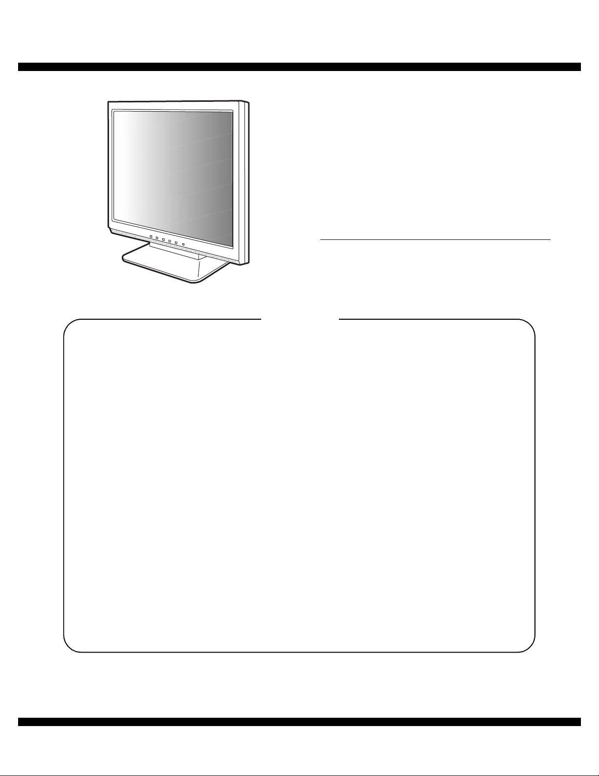
SERVICE MANUAL
MODEL
CONTENTS
CODE : 00Z
LLT15S3SME
LCD MONITOR
LL-T15S3
CHAPTER 1. OUTLINE OF THE PRODUCT,
NOMENCLATURE AND FUNCTION. . . . . . . . . . . . . . . . . .1 - 1
CHAPTER 2. CONNECTION, ADJUSTMENT,
OPERATION, AND FUNCTIONS. . . . . . . . . . . . . . . . . . . . .2 - 1
CHAPTER 3. DISASSEMBLY AND ASSEMBLY. . . . . . . . . . . . . . . . . . . .3 - 1
CHAPTER 4. TROUBLESHOOTING. . . . . . . . . . . . . . . . . . . . . . . . . . . . .4 - 1
CHAPTER 5. CONNECTOR SIGNAL TABLE •
CIRCUIT DIAGRAM • PWB LAYOUT . . . . . . . . . . . . . . . . .5 - 1
■ APPENDIX : IC DESCRIPTION . . . . . . . . . . . . . . . . . . . . . . . . . . . . . . .6 - 1
Parts marked with "!" are important for maintaining the safety of the set. Be sure to replace these parts with specified
ones for maintaining the safety and performance of the set.
This document has been published to be used
SHARP CORPORATION
for after sales servic e only.
The contents are subject to change without notice.
Page 2
CHAPTER 1. OUTLINE OF THE PRODUCT, NOMENCLATURE AND FUNCTION
1. SPECIFICATIONS
■
■ PRODUCT SPECIFICATIONS
■ ■
• LCD display
38 cm measured diagonally
TFT LCD module
• Resolution (max.)
XGA 1024 x 768 pixels
• Displayable colors (max.)
Approx.16.19 million colors (6bit + FRC)
• Brightness (max.)
260cd/m
• Dot pitch
0.297 (H) x 0.297 (V) mm
• Contrast ratio
350:1
• Angle of visibility
Left-right 160°; Up-down 150° (contrast ratio u 5)
• Screen display size
Horizontal 304.1 mm x Vertical 228.1 mm
• Video signal
Analog RGB (0.7Vp-p) [75Ω]
• Sync signal
Separate Sync (TTL level: +/-), Sync on Green,
Composite Sync (TTL level: +/-)
• Expansion compensation
Digital screening (Enlargement VGA/SVGA etc. to full screen size.)
• Plug & Play
VESA DDC1/DDC2B compatible
• Speaker output
1W + 1W
• Power management
VESA: based on DPMS
• Input signal terminal
Mini D-sub 15 pin (3 row)
• Audio input terminal
Mini stereo jack
• Headphone terminal
Mini stereo jack
• Screen tilt
Upward approx.0 - 25°; downward approx.0 - 5°
• Power supply
AC100 - 240V, 50/60Hz
• Temperature of operating environment
5 - 35°C
• Power consumption
33W (With no audio input)
(36W maximum, 2W when in power-saving mode)
• Dimensions
338 (W) x 145 (D) x 313 (H) mm
• Weight
Approx. 3.9kg (approx. 3.3kg excluding stand)
(Excluding analog signal cable.)
2
■
■ DIMENSIONS (UNITS: MM)
■ ■
338
275
313
203 145
63
Analog signal cable: Approx. 1.8m
Audio cable: Approx. 1.8m
■
■ SIGNAL TIMINGS
■ ■
Display mode Hsync Vsync Dot frequency
VESA 640 x 480 31.5kHz 60Hz 25.175MHz
37.9kHz 72Hz 31.5MHz
37.5kHz 75Hz 31.5MHz
800 x 600 35.1kHz 56Hz 36.0MHz
37.9kHz 60Hz 40.0MHz
48.1kHz 72Hz 50.0MHz
46.9kHz 75Hz 49.5MHz
1024 x 768 48.4kHz 60Hz 65.0MHz
56.5kHz 70Hz 75.0MHz
60.0kHz 75Hz 78.75MHz
US text 720 x 400 31.5kHz 70Hz 28.3MHz
Power
Macintosh
series
• Recommended resolution is 1024 x 768.
• All are compliant only with non-interlaced.
• Frequencies for Power Macintosh are reference values.
• If the monitor is receiving timing signals that are not compatible, [OUT
OF TIMING] will appear.
Follow your computer's instruction manual to set the timing so that it
is compatible with the monitor.
• If the monitor is not receiving any signal (synch signal), [NO SIGNAL]
will appear.
640 x 480 35.0kHz 66.7Hz 30.2MHz
832 x 624 49.7kHz 74.6Hz 57.3MHz
1024 x 768 60.2kHz 75Hz 80.0MHz
LL-T15S3 OUTLINE OF THE PRODUCT, NOMENCLATURE AND FUNCTION
1 – 1
Page 3
■
■ THE ANALOG RGB INPUT CONNECTOR PIN
■ ■
(Mini D-sub connector with 15 pins)
12345
10
6789
1112131415
No. Function No. Function
1 Red video signal input 9 +5V
2 Green video signal input 10 GND
3 Blue video signal input 11 N.C.
4 GND 12 DDC data
5 GND 13 For Hsync signal input
6 For red video signal GND 14 For Vsync signal input
7 For green video signal GND 15 DDC clock
8 For blue video signal GND
■
■ POWER MANAGEMENT
■ ■
The monitor is based on VESA DPMS (Display Power Management Signaling).
To activate the monitor's Power Management function, both the video
card and the comp uter must conform to the VESA DPMS standard.
DPMS mode Screen
ON Display on 36W Yes Yes
STANDBY
SUSPEND Yes No
OFF No No
■
■ DDC (PLUG & PLAY)
■ ■
This monitor supports the VESA DDC (Display Data Channel) standard.
DDC is a signal standard for carry ing out Plug & Play functions on the
monitor or PC. It transfers information such as degree of resolution
between the monitor and PC. You can use this function if your PC is DDC
compliant and if it is set so that it can detect the Plug & Play monitor.
There are many va rieties of DDC due to the d ifferences between sys tems. This monitor works with DDC1 and DDC2B.
Display off 2W
Power
consumption
H-sync V-sync
No Y es
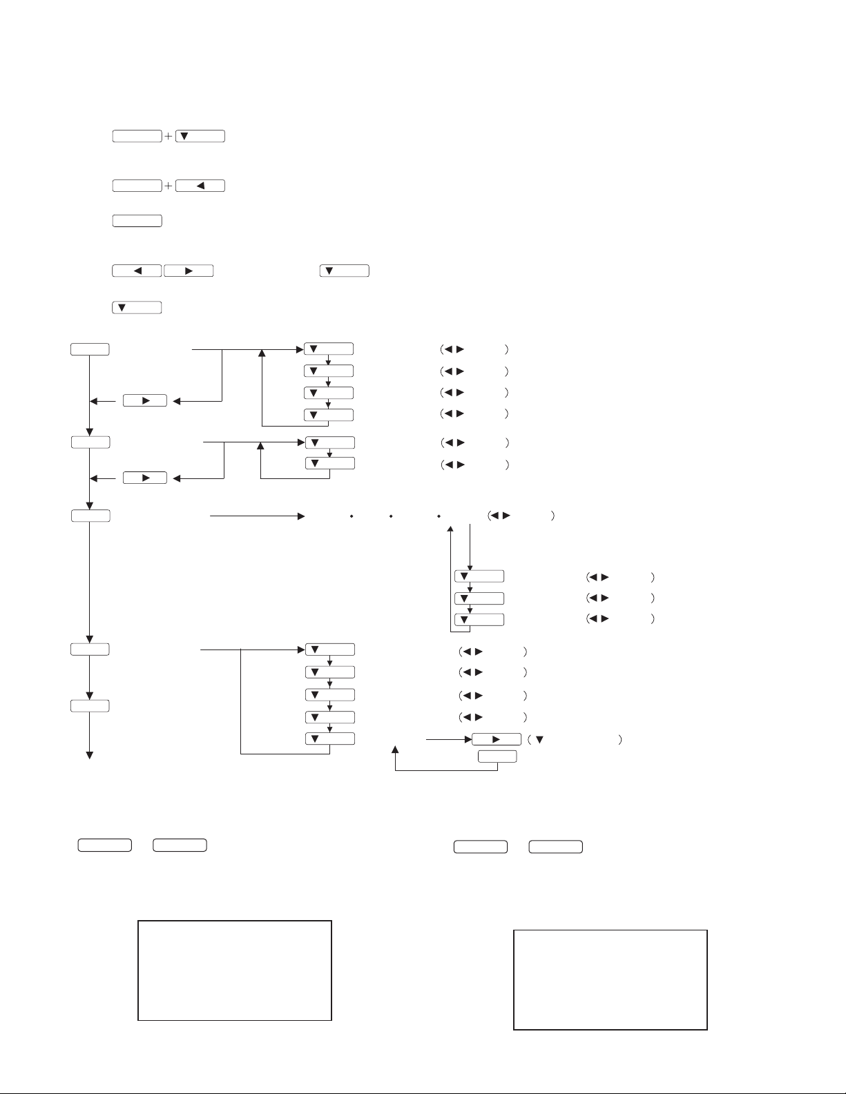
2. PRODUCT DESCRIPTION
1 2 3 4 5 66 7 8 9 1110
1. MENU button:
2. c/MODE button:
3. e d buttons:
4. Power button:
5. Power LED:
6. Speakers:
7. Power terminal:
8. Analog RGB input terminal:
9. Audio input terminal:
10. Security lock anchor:
11. Headphone terminal:
12. Ventilation openings:
This button is used to pop-up, select and close
the OSD (On Screen Display) Menu.
When the OSD Menu is displayed:
This button is used to select menu options.
When the OSD Menu is not displayed:
This button is used to set COLOR MODE.
When the OSD Menu is displayed:
These buttons are used to select an option or
adjust the value of the selected option.
When the OSD Menu is not displayed:
These buttons are used to adjust backlight
brightness and speaker volume.
Pressing this button turns the power on. (After
turning the power on, it may take a little time
before the screen displays.)
Press the button again to turn the power off.
This LED is lit green when in use and orange
when in power-saving mode.
Audio entering via the monitor and the external
device connected to the monitor can be heard.
The analog signal cable is connected here.
The analog signal cable included should be
used.
A computer’s audio output terminal can be
connected here. The audio cable included
should be used.
By connecting a security lock (commercially
available) to the security lock anchor, the monitor is fixed so that it cannot be transported.
The security slot works in conjunction with
Kensington Micro Saver Security Systems.
Headphones (commercially available) can be
connected here.
Note: Never block the ventilation openings as
this may lead to overheating inside the monitor
and result in malfunction.
12
LL-T15S3 OUTLINE OF THE PRODUCT, NOMENCLATURE AND FUNCTION
1 – 2
Page 4
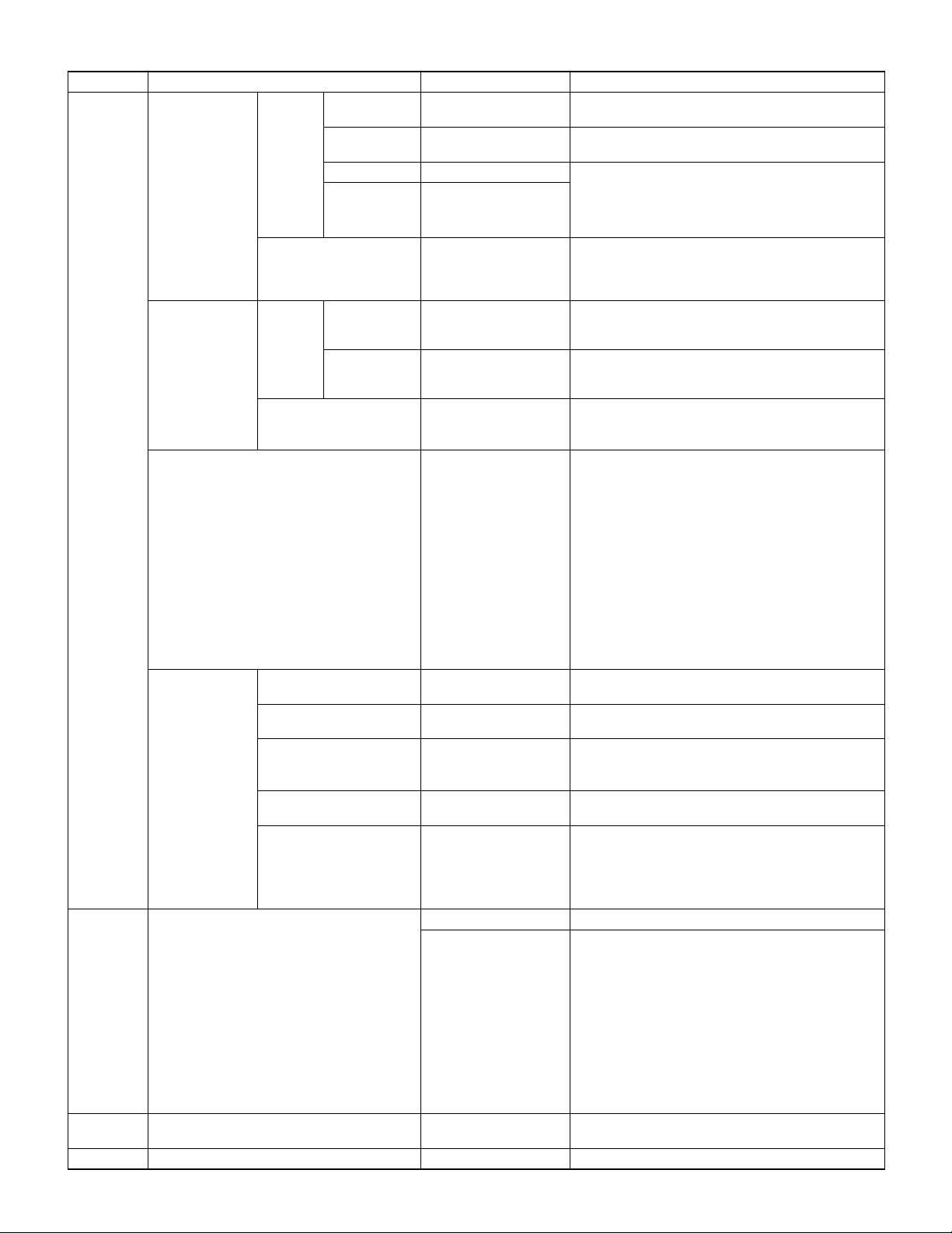
■
■ STANDING UP AND ADJUSTING THE MONITOR
■ ■
Caution:
• Pressur e from hands on the LCD panel could cause damage.
• Be careful not to allow your fingers to be pinched.
1) Standing up the monitor
1. Press down on the stand and lift up the top section of the monitor.
2) Angle adjustment
Press down on the stand and adjust it to a suitable viewing angle.
approx. 5 approx. 25
• Do not use the monitor when tilted back beyond approxim ately 25°.
The monitor may fall over leading to injury or malfunction.
• When raising the display section, move ment becomes harder in
the middle of travel.
Continue raising by applying more force at that point.
approx. 5
• Raise the display section until it stops. (when titled forward
approx. 5°)
2. Adjust to an easy to view angle.
approx. 5
approx. 25
Prohibited range
3) Folding up the monitor
1. Remove the cable.
2. Press down on the stand and gently fold back the monitor.
LL-T15S3 OUTLINE OF THE PRODUCT, NOMENCLATURE AND FUNCTION
1 – 3
Page 5
CHAPTER 2. CONNECTION, ADJUSTMENT, OPERATION, AND FUNCTIONS
1. CONNECTING THE MONITOR AND TURNING THE MONITOR ON AND OFF
Caution:
• When connecting, ensure that both the monitor and computer are switched off.
• Be careful not to overly bend the cable or add extension cords as this could lead to a malfunction.
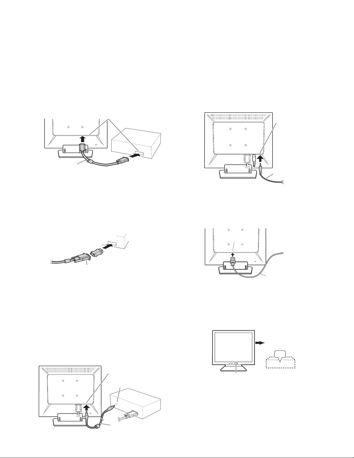
1-1. CONNECTING THE MONITOR TO A COMPUTER
Analog RGB terminal
(Mini D-sub 15 pin, 3 row)
Analog signal cable
• Paying attention to connector direction, firmly inse rt the signal cable
to terminal, and then tighten the screws at both sides.
If connecting to a D-sub 15 pin 2 row Apple Power Macintosh, attach a
Macintosh conversion adapter (commercially available) to the analog
signal cable.
1-2. CONNECTION OF HEADPHONES
(COMMERCIALLY AVAILABLE)
Headphones (commercially available) can be connected.
Headphone terminal
Headphones
Note: When the headphones are connected, no sound can be heard
from the monitor speakers.
1-3. CONNECTING THE MONITOR TO A POWER
SOURCE
Power terminalo
AC outlet
Macintosh conversion adapter
Note: When connecting to a notebook, if the notebook computer's
screen is set so that it is displaying at the same time, the MSDOS screen may not be able to display properly. In this case,
change the settings so that only the monitor is displaying.
■■■■ Connect the accessory audio cable
When the accessory audio cable is connected to the audio output terminal of the computer, the sound of the connected computer is output
from the monitor speakers. You can also use the headphone jack of the
display.
Audio input terminal
Audio output terminal
Audio cable
Power cord
1-4. TURNING THE POWER ON
1. Press the monitor's POWER button.
2. Turn on the computer.
The power LED will be lit green, and the screen will display an
image.
Turn on the
computer
ON
Press power button
Note:
• If us ing the monitor for the first time or after having changed the
system settings during use, perform an automatic screen adjustment.
• Depending on the computer or OS, it may be necessary to use the
computer to install monitor set-up information. If so, follow the
steps below to install the monitor set-up information.
LL-T15S3 CONNECTION, ADJUSTMENT, OPERATION, AND FUNCTIONS
2 – 1
Page 6
1-5. TURNING THE POWER OFF
1. Turn the computer off.
2. Press the monitor's POWER button.
The Power LED will disappear.
Turn the
computer off
OFF
Press power button
If the monitor is not going to be used for a long period of time, be sure to
unplug it from the AC outlet.
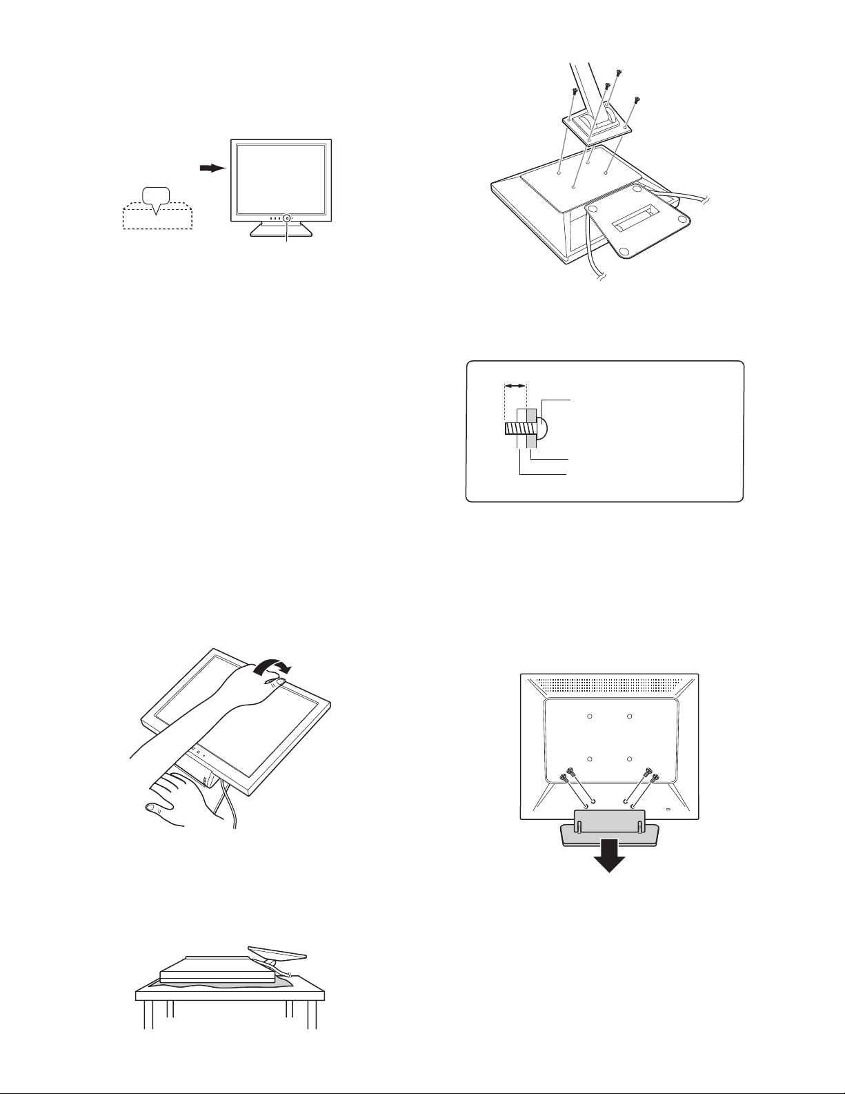
1-6. INSTRUCTIONS FOR ATTACHING A VESA
COMPLIANT ARM
An arm or stand based on the VESA standard (comme rcially available)
can be attached to the monitor.
Procurement of the arm or stand is at the custom-er's discretion.
When choosing the arm to be installed please take note of the following
points.
• The arm should be compatible with the VESA standard, and there
must be a gap of 75mm x 75mm between the screw holes on the
section to be attached.
• The arm m ust not fall off or break off after being attached to the
monitor.
1. Ensure that both the monitor and computer are switched off.
2. Unplug the power cord from the AC outlet.
3. Remove the analog signal cable and the audio cable from the computer.
4. Press down on the stand and gently fold back the monitor.
6. Attach the arm to the monitor with four screws.
Note: The screws used to attach the arm should be M4 screws with a
length of 8 mm ~ 10 mm protruding from the surface to be
attached. Using different screws could cause the monitor to fall o ff
or to be internally damaged.
8~10mm
Screw used to attach arm
Arm
Part of monitor to which arm is
attached
7. Connect the analog signal cable and power cord.
The stand may be removed.
1. Turn off the monitor, and remove the analog signal cable, the audio
cable and the power cord from the monitor.
2. Being careful not to damage the monitor, spread out a soft cl oth and
lay the monitor on it display-side down.
3. Remove the four screws and then remove the stand from the monitor.
• Be careful not to allow your fingers to be pinched.
• Do not overly bend the cable or add extension cords as this could
lead to malfunction.
5. Being careful not to damage the monitor, spread out a soft cloth and
lay the monitor on it display-side down.
LL-T15S3 CONNECTION, ADJUSTMENT, OPERATION, AND FUNCTIONS
• The stand is specially made for use with this monitor. Once having removed the stand, never attempt to attach it to another
device.
• Once having removed the screws, store them together with the
stand and if the stand is ever re-attached be sure to use the original screws.
Using different screws could lead to a malfunction.
4. Follow instruction no.6 to attach the arm to the monitor, then connect the analog signal cable, the audio cable and the power cord.
2 – 2
Page 7
2. ADJUSTMENT
2-1. ADJUSTMENT METHOD
1) Resetting all adjustment values
MENU
Press the above two buttons at same time, and while turn the power on.
2) ADJUSTMENT menu reset
MENU
3) Adjustment lock function
MENU
While pressing the MENU button, turn the power on.
4) Adjusting the backlight and speaker volume
5) Setting color mode
/MODE
6) Screen adjustment
MENU
ADJUSTMENT
AUTO
/MODE
Power ON
Press the two buttons at same time.
Power ON
buttons (Press the button and select "BRIGHT" or "VOLUME".)
button (STD, sRGB, VIVID)
/MODE
/MODE
/MODE
/MODE
/MODE
CLOCK
PHASE
H-POS
V-POS
buttons
buttons
buttons
buttons
MENU
GAIN CONTROL
/MODE
/MODE
AUTO
MENU
MENU
MENU
MODE SELECT
WHITE BALANCE
(COOL STD
/MODE
/MODE
/MODE
/MODE
/MODE
END
6) Version display (for service)
MENU d
Power ON
Display the software version.
Press the above two buttons at same time, and while turn the power
on.
BLACK LEVEL
CONTRAST
WARM USER)
OSD H-POSITION
OSD V-POSITION
SCALING
COLORS
LANGUAGE
7) A g ing (for service )
buttons
buttons
buttons
CONTRAST
(R/G/B)
/MODE
/MODE
/MODE
R-CONTRAST
G-CONTRAST
B-CONTRAST
buttons
buttons
buttons
buttons
buttons
buttons
buttons
/MODE
buttons
MENU
c /MODE e
Power ON
Press the d button, Screen color is changed as following.
Green 3 Blue 3 Gray 3 White 3 Light Red 3 Light Green 3
Pink 3 Red
When the test is terminate, Power off
<VERSION & CHECK SUM>
VERSION : 1.01 (200XXXXX)
CHECK SUM : OK XXXX
LL-T15S3 CONNECTION, ADJUSTMENT, OPERATION, AND FUNCTIONS
AGING TEST
> : SET
MENU : END
2 – 3
Page 8
2-2. ADJUSTMENT ITEM LIST
BUTTON ITEM ADJUSTMENT DESCRIPTION
MENU MENU 1:
ADJUSTMENT
MENU 2:
GAIN CONTROL
MENU 1
4
MENU 2
4
MENU 3
4
MENU 4
4
MENU END
MENU 3:
WHITE BALANCE
MENU 4:
MODE SELECT
/MODE
c
e d
POWER OFF
MANUAL CLOCK 0~255 CLOCK:Adjust so that vertical flicker noise is not emit-
ted. (e d buttons)
PHASE 0~31 PHASE: Adjust so that horizontal flicker noise is not
H-POS 0~400
V-POS 0~100
emitted. (e d
H-POS (horizontal positioning) and
V-POS (vertical pos it ioning)
To center the screen image within the boundaries of
e d buttons)
e de d
the screen, adjust the left-right (H- POS) values and
the up-down (V-POS) values. (e d
AUTO Automatic screen adjustment
Options in the ADJUSTMENT Menu can be adjusted
automatically
(CLOCK, PHASE, H-POS V-POS).
MANUAL BLACK LEVEL 0~63
BLACK LEVEL: Total screen brightness can be adjusted
while watching the color pattern.
e d
buttons)
(
CONTRAST 0~100 CONTRAST: While watching the color pattern,
adjustments can be made so that all
graduations appear. (e d
AUTO GAIN CONTROL Menu
AUTO:Every menu option is automatically adjusted
using the Auto Gain Control function.
COOL • STD • WARM
(5 levels),
USER R • G • B: 0~100
WHITE BALANCE Menu
COOL : Color tone bluer than standard
• : Color tone slightly bluer than standard
STD : Color tone standard setting
• : Color tone slightly redder than standard
WARM : Color tone redder than standard
USER
R-CONTRAST: e button for blue-green
d button for red
G-CONTRAST: e button for purple
d button for green
B-CONTRAST: e button for yellow
d button for blue
OSD H-POSITION
(OSD horizontal position)
OSD V-POSITION
(OSD vertical position)
SCALING
(Level of scaling)
LOW • HIGHT SCALING (Level of scaling)
The position of the OSD display can be moved to the
left and right. (e d buttons)
The position of the OSD displa y can be moved up an d
down. (e d buttons)
Adjusts the image to optimum sharpness when Screen
expansion is taken. (e dbuttons)
COLORS
260K (approx . 260,000)
Maximum display colors can be set. (e dbuttons)
16M (approx. 16.19million)
LANGUAGE 7 countrys
DEUTSCH, ENGL ISH,
ESPANOL, FRANCAIS,
ITALIANO, NETHERLAND, SVENSKA
LANGUAGE
Messages displayed on the scree n and OSD Menu
contents can be changed to the following languages.
Dutch, English, French, German, Spanish, Italian,
Swedish.
Select the item
sRGB, STD, VIVID Setting color mode when the ADJUSTMENT Menu is
not displayed.
STD: Displays image with the color tone results from
original scheme of liquid crystal panel.
sRGB: sRGB is international standard of color repre-
sentation specified by IEC (International Electrotechnical Commission). Color conversion is
made in taking account of liquid crystals characteristics and represents color tone close to it
original image.
VIVID: Displays an image with dynamic and VIVID pri-
mary colors.
Volume: 0~100
Adjusting the backlight and speaker volume
Bright: 0~31
e d buttons)
e de d
e d buttons)
e de d
LL-T15S3 CONNECTION, ADJUSTMENT, OPERATION, AND FUNCTIONS
2 – 4
Page 9

CHAPTER 3. DISASSEMBLY AND ASSEMBLY
1. SEPARATING DISPLAY UNIT AND
STAND UNIT
1) Remove the screws and separate the display unit 1 from the stand
unit 2.
2
1
2. REMOVING KEY BOARD
1) Remove the screws and then remove t he rear cabinet .
2) Remove the screws A and the n remove th e ground l ead.
3) Remove the connectors and screws B, and then remove the power
supply/inverter board .
B
B
B
A
B
4) Remove the connector lo ckin g tape.
5) Remove the conne ctors an d screws, and then remove t he main boar d.
2) Remove the screws and connectors, and then remove the KEY board.
3. REMOVING POWER SUPPLY/INVERTER
BOARD AND MAIN BOARD
1) Remove the hex. screws A and screws B, and then r emove the shield.
B
B
B
B
A
B
B
4. REMOVING LCD MODULE
1) Remove the screws A and the n remove th e front cabi ne t 1.
2) Remove the screws B, and then remove the frame 2 from the LCD
module 3.
A
B
2
B
3
1
A
B
B
LL-T15S3 DISASSEMBLY AND ASSEMBLY
3 – 1
Page 10

CHAPTER 4. TROUBLESHOOTING
No power supply
Does LED turns on in green
when power switch is turned
on?
Yes
Backlight turns ON?
Yes
Check for RGB cable input
signal.
A
Normal
Replace RGB cable.
Defective
No
No
Check each pin terminal
of P3.
Normal
No output +5V, 12V from
power supply unit.
LED turns on in red?
No
LED turns on in orange?
No
Yes
Yes
Yes
Replace power supply unit.
Check LED for breakage.
*
Check key cable for disconnection.
*
Yes
Replace any unit (main PWB, SW PWB, cable)
which shows any defect, with a new one.
Check whether the unit is in power save
mode (synchronizing signal is not input.).
1) PC is turned off?
2) RGB cable is disconnected?
3) Synchronizing signal is output from RGB
cable?
No
Synchronizing signal is input to main PWB?
Yes
No
Check inverter PWB unit.
*
Note: Use caution when checking output
side because it has a high voltage.
Normal
Replace LCD module lamp with
a new one.
Defective
Replace inverter PWB
unit with a new one.
LL-T15S3 TROUBLESHOOTING
Replace RGB cable
with a new one.
Check power input system.
1) Power supply PWB
* Normal?
* Connected properly?
2) Blown out fuse (F1)?
3) Check +5VX, 3.3VX, 3.3VA, VDD, VD
and VLCD are output?
4) LED
* Check LED for breakage.
* Check the path between P5 and U6.
* Check the cable for disconnection.
Yes
Replace any defective unit.
[ 1) Power supply PWB, 2) Main PWB,
3) Switch PWB] with a new one.
4 – 1
Page 11

Screen does not operate normally.
Check screen condition by changing display modes.
Operate the "ALL RESET" to check if screen condition changes.
(Press and hold MENU and SELECT buttons while turning on power switch.)
A
Screen stays in black. Screen stays in white.
Check RGB cable.
Screen jitters or on-screen
characters flicker.
Defective
Replace RGB cable with
a new one.
Abnormal color
Check the following signals
1) Check if module control signal is output (U1).
2) Check if VLCD voltage is output normally.
Yes No
Main PWB defective.
CLOCK and PHASE
can be adjusted?
Yes No
Switch PWB defective
LL-T15S3 TROUBLESHOOTING
4 – 2
Does abnormal area move on
screen when BLACK LEVEL or
CONT is changed after H-POS
or V-POS is set?
Yes No
LCD panel defective.
Page 12

CHAPTER 5. CONNECTOR SIGNAL TABLE • CIRCUIT DIAGRAM • PWB LAYOUT
1. CONNECTOR SIGNAL TABLE
CONNECTOR P1 CONNECTOR P2 CONNECTOR P3
1GND
2BO7
3BO6
4BO5
5BO4
6GND
7BO3
8BO2
9BO1
10 BO0
11 GND
12 GO7
13 GO6
14 GO5
15 GO4
16 GND
17 GO3
18 GO2
19 GO1
20 GO0
21 GND
22 RO7
23 RO6
24 RO5
25 RO4
26 GND
27 RO3
28 RO2
29 RO1
30 RO0
31 GND
32 GND
33 N.C
34 N.C
35 N.C
36 GND
1GND
2 DCLK
3GND
4DE-O
5VSYNC
6HSYNC
7N.C
8GND
9BE7
10 BE6
11 BE5
12 BE4
13 GND
14 BE3
15 BE2
16 BE1
17 BE0
18 GND
19 GE7
20 GE6
21 GE5
22 GE4
23 GND
24 GE3
25 GE2
26 GE1
27 GE0
28 GND
29 RE7
30 RE6
31 RE5
32 RE4
33 GND
34 RE3
35 RE2
36 RE1
37 RE0
38 VLCD
39 VLCD
40 GND
1 12V
2GND
3GND
45V
5 BRI_Min
6INV_ON
CONNECTOR P5
1POW1
2GND
3LED1
4LED2
5 KEY1
6 KEY2
7 KEY3
8 KEY4
CONNECTOR P8
1Red
2 Green
3 Blue
4 Ground
5 Ground
6R-GND
7 G-GND
8B-GND
9+5V
10 Ground
11 N.C
12 (SDA)
13 H-sync
14 V-sync
15 (SCL)
LL-T15S3 CONNECTOR SIGNAL TABLE • CIRCUIT DIAGRAM • PWB LAYOUT
5 – 1
Page 13

D
C
B
A
1/4
12345678
21
3
2. CIRCUIT DIAGRAM
87654
2-1. MAIN PWB
D
LL-T15S3 CONNECTOR SIGNAL TABLE • CIRCUIT DIAGRAM • PWB LAYOUT
C
5 – 2
B
A
Page 14

D
C
B
A
2/4
12345678
2 1
3
8 7 6 5 4
D
LL-T15S3 CONNECTOR SIGNAL TABLE • CIRCUIT DIAGRAM • PWB LAYOUT
C
5 – 3
B
A
Page 15

D
C
B
A
3/4
12345678
2 1
3
8 7 6 5 4
D
LL-T15S3 CONNECTOR SIGNAL TABLE • CIRCUIT DIAGRAM • PWB LAYOUT
C
5 – 4
B
A
Page 16

D
C
B
A
4/4
12345678
2 1
3
8 7 6 5 4
D
LL-T15S3 CONNECTOR SIGNAL TABLE • CIRCUIT DIAGRAM • PWB LAYOUT
C
5 – 5
B
A
Page 17

12345678
12345678
12345678
12345678
BD1
2
Y1
F2
FUSE- 2A /250V
12
D18
D19
2KBP06M
L1
P6KE160A
P6KE160A
UU15.7
12
1000P
CN1
1/1
CN2
L4
DR 8*10
C41
2n2/500V
R51
1/4W100
R50
1/4W100
T3
EFD25
21
21
R38
1
4
Y3
4
2
1
3
R36
1/2W
1M
X1
10N
VZ1
123
12
11023
C53
1/4W 750K
332P
0.47uF
471
Y2
+12V/2.0A
GND
GND
12345
R54
1/4W 5.6K
470uF/25V(KY)
10*16
+
C42
12.5*20
C38
1000uF/25V(KY)
+
C36
2n2/500V
R53
1
32
D16
20A100V
1/4W 100
6
2n2/1KV
D13
EGP10M
R39
1/4W 750K
C33
18*3 2
+
100U/400V(KMG)
3
RT1
2A 4R (P = 5 m m)
1000P
F3
FUSE- 2A /250V
12
+5V/1.8A
BRIGHTNESS
EN_ON
6
470U/25V(KY)
C43
10* 16
+
L6
12
DR 8 *10
C40
10*16
+
C51
2n2/500V
C37
2n2/500V
R52
1
1/4W 100
D17
10A/60V
32
9
8
7
5
4
C39
101P/1KV
21
23
Q12
2SK2628
T0-220F
R40
D
D
D
D
INV TO M/B CON
470U/25V(KY)
D14
RGP10D
DO41
21
FB4
12
1
10R(1/4W)
Secondary GND
R90
12
1/4W
FB3
R55
1/4W 820
1
U4
4
R44
U2SG6841
GATE
GNDFBVIN
123
Primary GND
R75
23
PC-621
1/4W
15R
0.39
1WS
R43
678
VDD
R78
Q15
2SA673
R89
R77
R76
1/2W 1k
U6
TL431
1K
1/2W
312
R73
R74
105K
1/8W
1/8W
24.9K
U5
TL431
312
103P
C44
R58
1/8W 5.6K
1/8W
R59
7K
R56
1/8W
13.
R57
1/8W
+
C34
5*11
10uF/50V(KY)
R42
1/8W
SENSE
RI RT
45
Fosc=5 0KHz
1/8W
R41
33K
B
B
B
13
D10
DAN217
13
D9
DAN217
5
SI4532
Q11
4
R22
xxxx
CP
CP
C18
C17
RT
0R
TP
1817161514
CT
RT
PWRGND
ENA
SST
VDDA
C5
0.47U
680n
C4
470n
C52
C3
10n
R4
10K
EN_ON
2
2
876
123
63.4K/F
C20
3.3nF
3.3nF(5%)
C19
TP
DIM
LCT
OZ960
REF
GNDA
6
7199
C7
C6
1.0U/25V/1206
R13280K,1%
XXXX
B
R34
560
R35
422R/1%
CP
21
D4
1M
0.1U
R18
2
Q7
3
21
LL4148
D3
R15
+5V
FB1
LL4148
21
D5
47K
2N7002
1
51K
C10
C/NC
Q4
10k
R7
LL4148
C11
MMBT3904
LL4148
CP
OPEN
123
31
Q5
D1
CN4
R16
2
21
OP1
R86
15K 1%
Vhigh-2(Lamp2)
Vhigh-1(Lamp1)
1
2
SM02B-BHSS-1-TB(JST)
R28
C24
8
9
15P,3KV
5,6,7
1,2,3,4
C15
4.7U,X5R,10V
220u/25V
+ C14
B+
10K
2N7002
C12
0.22U
R8
1M
Vlow-1(Lamp1)
CN6
3M(SMD/2010)
C25
T2
19:2600
C46
4.7u/10V(X5R/1206)
876
Q8
123
OP1
OVP
5
SI4532
P_C
4
ZD4
5.6v
R27
10K
C23
R26
C22
0.047U
N_D
0.1U
C21
0R
R230RR24
138
12
11
U1OZ960G/SSOP20
LPWMRT1
PDRV_C
NDRV_D
FB
CMP
10
C9
C8
10n
R14
1500P(NPO)
R17 18K
NC
0.1U
RT
C
C
C
C
Vhigh-2(Lamp2)
Vhigh-1(Lamp1)
Vlow-1(Lamp1)
Vlow-2(Lamp2)
2
1
2
2
1
CN3
220R/3W
220R/3W
220R/3W
R60
1/8W 330
R61
13.3K
Pin 2
R46
1/8W 1K
R45
1/8W 10K
ZD7
ZD6
21
21
1/2W 16-2
R57
1/8W
1
2
U3
PC-6 21
3
4
ZD5
26V
21
21
D15
1N4148
Q14
TO-9 2
2SC1815
1/8W
R48
100K
R47
1/8W 100K
C35
0.1uf
Q13
TO-92
2SA1015
TP
TP
C28
4.7U,X5R,10V(1206)
1/8W 100
1/2W 6B2
R49
1K(1/8W)
C1
+
B+
F1
3A/DIP(R25103)
TP
CN5
SM02B-BHSS-1-TB(JST)
TP
R32
3M(SMD/2010)
C29
15P,3KV
C30
8
9
T1
19:2600
5,6,7
1,2,3,4
C45
4.7u/10V(X5R)1206
P_A
ZD3
R25
220U/25V(DIP)
TP
B+
R1
910R/1206
SM02(4.0)B-BHS-1-TB(JST)
D11
DAN217
TP
R33
C32
C31
6.8nF
10P,3KV
C49
10P/3KV
5.6v
C16
10K
R19
R10
137K/F
BRIGHTNESS
R2
560R/1206
Q1
Q2
DTA114EKA
Q3
DTC114EKA
13
3.32KF
560pF(NPO)
876
Q10
123
R87
N_B
0.047U
220P
0R
R20
R21
20
36.5K/F
PDRV_A
NDRV_B
CTIMR
OVP
12345
R11
110K/F
R3
22(1206)
+5V
904
123
MMBT3
5.6v
ZD1
123
R12
1M(0805)
C47
100n(0805)
2
Vlow-2(Lamp2)
1
2
SM02(4.0)B-BHS-1-TB(JST)
R29
C48
10P,3KV
10P/3KV
5
SI4532
4
P_A
N_B
2N7002
31
Q6
2
21
D2
LL4148
OP2
A
OP2
R30
560R(1206)
DAN217
13
3.32KF
560p(NPO)
C27
C26
6.8nF
876
5
Q9
123
4
N_D
C13
0.22U D8
R9
1M
21
21
21
21
3
3
3
3
R85
FB1
15K
CP
CP
R31
422R/1%
13
D7
DAN217
2
13
D6
DAN217
2
OVP
SI4532
P_C
R68,R71,R69,R72,R64,R65,R67,R83,R80(0805) 0R
R66,R67,R70,R79,R81,R84 (1206)0R
J8,J9,J10,J11,J12,J13,J14,J15,J16,J17,J18,J19, J20,J21
J22,J25,J26,J28
87654
87654
87654
87654
2-2. POWER SUPPLY PWB
B
B
B
D
D
D
D
C
C
C
C
B
LL-T15S3 CONNECTOR SIGNAL TABLE • CIRCUIT DIAGRAM • PWB LAYOUT
5 – 6
A A
A A
A A
A
Page 18

3. PWB LAYOUT
3-1. MAIN PWB
A side
LL-T15S3 CONNECTOR SIGNAL TABLE • CIRCUIT DIAGRAM • PWB LAYOUT
5 – 7
Page 19

B side
LL-T15S3 CONNECTOR SIGNAL TABLE • CIRCUIT DIAGRAM • PWB LAYOUT
5 – 8
Page 20

3-2. POWER SUPPLY PWB
LL-T15S3 CONNECTOR SIGNAL TABLE • CIRCUIT DIAGRAM • PWB LAYOUT
5 – 9
Page 21

■■■■APPENDIX : IC DESCRIPTION
1. PIN DESCRIPTION
1-1. PIN LAYOUT
TVCLK
IRQ#
SCS#
SDA
SCL
RST
GPIO1
GPIO0
DCVSS
CONFIG4
154
153
DIBVDD
CAP_HREF
CAP_HSYNC
CAP_VSYNC
DIBVSS
BLU_INB_0/Y0
BLU_INB_1/Y1
BLU_INB_2/Y2
BLU_INB_3/Y3
BLU_INB_4/Y4
BLU_INB_5/Y5
BLU_INB_6/Y6
BLU_INB_7/Y7
DCVDD
GRN_INB_0
GRN_INB_1
GRN_INB_2
GRN_INB_3
GRN_INB_4
GRN_INB_5
GRN_INB_6
GRN_INB_7/RTS0
DCVSS
RED_INB_0/UV0
RED_INB_1/UV1
RED_INB_2/UV2
RED_INB_3/UV3
RED_INB_4/UV4
RED_INB_5/UV5
RED_INB_6/UV6
RED_INB_7/UV7
DIBVDD
DVDD
DVSS
DTEST
VCCD
DGND
VGA_VSYNC
VGA_HSYNC
SOGI
160
159
158
1
2
3
4
5
6
7
8
9
10
11
12
13
14
15
16
17
18
19
20
21
22
23
24
25
26
27
28
29
30
31
32
33
34
35
36
37
38
39
40
157
414243444546474849505152535455565758596061626364656667686970717273747576777879
152
156
155
MascotV
CONFIG3
151
150
CONFIG2
CONFIG1
CONFIG0
149
148
147
PWM0
PWM1
146
145
DCVDD
LCD_VEE
144
143
LCD_VDD
LCD_VBL
DCVSS
142
141
140
RED_OUTB_7
RED_OUTB_6
RED_OUTB_5
RED_OUTB_4
DOBVDD
138
137
136
135
139
RED_OUTB_3
RED_OUTB_2
RED_OUTB_1
RED_OUTB_0
DOBVSS
131
134
133
132
GRN_OUTB_7
GRN_OUTB_6
GRN_OUTB_5
130
129
128
127
GRN_OUTB_4
DOBVDD
GRN_OUTB_3
GRN_OUTB_2
GRN_OUTB_1
123
122
126
125
124
GRN_OUTB_0
121
120
DOBVSS
119
BLU_OUTB_7
118
BLU_OUTB_6
117
BLU_OUTB_5
116
BLU_OUTB_4
115
DOBVDD
114
BLU_OUTB_3
113
BLU_OUTB_2
112
BLU_OUTB_1
111
BLU_OUTB_0
110
DOBVSS
109
RED_OUTA_7
108
RED_OUTA_6
107
RED_OUTA_5
106
RED_OUTA_4
105
DCVDD
104
RED_OUTA_3
103
RED_OUTA_2
102
RED_OUTA_1
101
RED_OUTA_0
100
DCVSS
99
GRN_OUTA_7
98
GRN_OUTA_6
97
GRN_OUTA_5
96
GRN_OUTA_4
95
DOBVDD
94
GRN_OUTA_3
93
GRN_OUTA_2
92
GRN_OUTA_1
91
GRN_OUTA_0
90
DOBVSS
89
BLU_OUTA_7
88
BLU_OUTA_6
87
BLU_OUTA_5
86
BLU_OUTA_4
85
DOBVDD
84
BLU_OUTA_3
83
BLU_OUTA_2
82
BLU_OUTA_1
81
BLU_OUTA_0
80
VCCA
VREF
AGND
BI
CZ
CP
VCCAB
GNDAB
GI
VIOP
BCLP
VBOT
VCCAG
GNDAG
LL-T15S3 APPENDIX : IC DESCRIPTION
GCLP
TOUTP
TOUIM
VCCAR
RI
RCLP
RNDAR
ADVSS
ADVDD
DCVSS
OSD_FSW
OSD_R
OSD_G
OSD_CLK
OSD_I
OSD_B
XTALO
DCVDD
RESERVED
XTALI
DIBVSS
SHCLK
DISP_DE
DISP_VSYNC
DISP_HSYNC
DCVSS
6 – 1
Page 22

1-2. PIN DESCRIPTION
Pin
No.
Name Type Definition
001 DIBVDD Digital Input Buffer Power
002 CAP_HREF I Port B Horizontal Active Qualifier
003 CAP_HSYNC I Port B Horizontal Sync Input
004 CAP_VSYNC I Port B Vertical Sync Input
005 DIBVSS Ground Digital Input Buffer Ground
006 BLU_INB_0/Y0 I Port B Blue Input Bit 0/YUV Data Input
Y0
007 BLU_INB_1/Y1 I Port B Blue Input Bit 1/YUV Data Input
Y1
008 BLU_INB_2/Y2 I Port B Blue Input Bit 2/YUV Data Input
Y2
009 BLU_INB_3/Y3 I Port B Blue Input Bit 3/YUV Data Input
Y3
010 BLU_INB_4/Y4 I Port B Blue Input Bit 4/YUV Data Input
Y4
011 BLU_INB_5/Y5 I Port B Blue Input Bit 5/YUV Data Input
Y5
012 BLU_INB_6/Y6 I Port B Blue Input Bit 6/YUV Data Input
Y6
013 BLU_INB_7/Y7 I Port B Blue Input Bit 7/YUV Data Input
Y7
014 DCVDD Power Digital Core Power
015 GRN_INB_0 I Port B Green Input Bit 0
016 GRN_INB_1 I Port B Green Input Bit 1
017 GRN_INB_2 I Port B Green Input Bit 2
018 GRN_INB_3 I Port B Green Input Bit 3
019 GRN_INB_4 I Port B Green Input Bit 4
020 GRN_INB_5 I Port B Green Input Bit 5
021 GRN_INB_6 I Port B Green Input Bit 6
022 GRN_INB_7/
I Port B Green Input Bit 7
RTS0
023 DCVSS Ground Digital Core Ground
024 RED_INB_0/
UV0
025 RED_INB_1/
UV1
026 RED_INB_2/
UV2
027 RED_INB_3/
UV3
028 RED_INB_4/
UV4
029 RED_INB_5/
UV5
030 RED_INB_6/
UV6
031 RED_INB_7/
UV7
I Port B Red Input Bit 0/YUV Data Input
UV0
I Port B Red Input Bit 1/YUV Data Input
UV1
I Port B Red Input Bit 2/YUV Data Input
UV2
I Port B Red Input Bit 3/YUV Data Input
UV3
I Port B Red Input Bit 4/YUV Data Input
UV4
I Port B Red Input Bit 5/YUV Data Input
UV5
I Port B Red Input Bit 6/YUV Data Input
UV6
I Port B Red Input Bit 7/YUV Data Input
UV7
032 DIBVDD Power Digital Input Buffer Power
033 DVDD Power Digital VDD
034 DVSS Ground Digital ground
035 DTEST O Digital test output
036 VCCD Power Digital power
037 DGND Ground Digital ground
Pin
No.
Name Type Definition
038 VGA_VSYNC I Port A vertical SYNC
039 VGA_HSYNC I Port A horizontal SYNC
040 SOGI I Port A Sync-On-Green input
041 VCCA Power Analog power for PLL
042 AGND Ground Analog ground for PLL
043 VREF I External 25V reference voltage
044 CP I PLL loop filter for pole
045 CZ I PLL loop filter for zero
046 VCCAB Power B channel analog power
047 BI I B channel analog input
048 GNDAB Ground B channel analog ground
049 BCLP O B channel internal clamp voltage out-
put
050 VTOP O ADC resistor ladder top decoupling
capacitor
051 VBOT O ADC resistor ladder bottom decou-
pling capacitor
052 VCCAG Power G channel analog power
053 GI I G channel analog input
054 GNDAG Ground G channel analog ground
055 GCLP O G channel internal clamp voltage out-
put
056 TO UTP O Differential testing output plus
057 TO UTM O Differential testing output minus
058 VCCAR Power R channel analog power
059 RI I R channel analog input
060 RNDAR Ground R channel analog ground
061 RCLP O R channel internal clamp voltage out-
put
062 ADVDD
Power Display PLL Analog Power
(VDD_PLL)
063 ADVSS
Ground Display PLL Analog Ground
(VSS_PLL)
064 DCVSS Ground Digital Core Ground
065 OSD_FSW I External OSD Window Display Enable
066 OSD_CLK O Clock Output For External OSD Con-
troller Chip
067 OSD_R I R Data Input From External OSD Con-
troller Chip
068 OSD_G I G Data Input From External OSD Con-
troller Chip
069 OSD_B I B Data Input From External OSD Con-
troller Chip
070 OSD_I I Intensity Input From Ext OSD Control-
ler Chip
071 DCVDD Power Digital Core Power
072 Reserved R Reserved
073 XTAL O Crystal Out
074 XTALI I Crystal Input
075 DIBVSS Ground Digital Input Buffer Ground
076 DISP_DE O Display Enable
077 DISP_VSYNC O Display Vertical Sync
LL-T15S3 APPENDIX : IC DESCRIPTION
6 – 2
Page 23

Pin
No.
Name Type Definition
078 SHCLK O Shift Clock
079 DISP_HSYNC O Display Horizontal Sync
080 DCVSS Ground Digital Core Ground
081 BLU_OUTA_0 O Display Port A Blue Output Bit 0
082 BLU_OUTA_1 O Display Port A Blue Output Bit 1
083 BLU_OUTA_2 O Display Port A Blue Output Bit 2
084 BLU_OUTA_3 O Display Port A Blue Output Bit 3
085 DOBVDD Power Digital Output Buffer Power
086 BLU_OUTA_4 O Display Port A Blue Output Bit 4
087 BLU_OUTA_5 O Display Port A Blue Output Bit 5
088 BLU_OUTA_6 O Display Port A Blue Output Bit 6
089 BLU_OUTA_7 O Display Port A Blue Output Bit 7
090 DOBVSS Ground Digital Output Buffer Ground
091 GRN_OUTA_0 O Display Port A Green Output Bit 0
092 GRN_OUTA_1 O Display Port A Green Output Bit 1
093 GRN_OUTA_2 O Display Port A Green Output Bit 2
094 GRN_OUTA_3 O Display Port A Green Output Bit 3
095 DOBVDD Power Digital Output Buffer Power
096 GRN_OUTA_4 O Display Port A Green Output Bit 4
097 GRN_OUTA_5 O Display Port A Green Output Bit 5
098 GRN_OUTA_6 O Display Port A Green Output Bit 6
099 GRN_OUTA_7 O Display Port A Green Output Bit 7
100 DCVSS Ground Digital Core Ground
101 RED_OUTA_0 O Display Port A Red Output Bit 0
102 RED_OUTA_1 O Display Port A Red Output Bit 1
103 RED_OUTA_2 O Display Port A Red Output Bit 2
104 RED_OUTA_3 O Display Port A Red Output Bit 3
105 DCVDD Power Digital Core Power
106 RED_OUTA_4 O Display Port A Red Output Bit 4
107 RED_OUTA_5 O Display Port A Red Output Bit 5
108 RED_OUTA_6 O Display Port A Red Output Bit 6
109 RED_OUTA_7 O Display Port A Red Output Bit 7
110 DOBVSS Power Digital Output Buffer Ground
111 BLU_OUTB_0 O Display Port B Blue Output Bit 0
112 BLU_OUTB_1 O Display Port B Blue Output Bit 1
113 BLU_OUTB_2 O Display Port B Blue Output Bit 2
114 BLU_OUTB_3 O Display Port B Blue Output Bit 3
115 DOBVDD Power Digital Output Buffer Power
116 BLU_OUTB_4 O Display Port B Blue Output Bit 4
117 BLU_OUTB_5 O Display Port B Blue Output Bit 5
118 BLU_OUTB_6 O Display Port B Blue Output Bit 6
119 BLU_OUTB_7 O Display Port B Blue Output Bit 7
120 DOBVSS Ground Digital Output Buffer Ground
121 GRN_OUTB_0 O Display Port B Green Output Bit 0
122 GRN_OUTB_1 O Display Port B Green Output Bit 1
123 GRN_OUTB_2 O Display Port B Green Output Bit 2
124 GRN_OUTB_3 O Display Port B Green Output Bit 3
125 DOBVDD Power Digital Output Buffer Power
126 GRN_OUTB_4 O Display Port B Green Output Bit 4
Pin
No.
Name Type Definition
127 GRN_OUTB_5 O Display Port B Green Output Bit 5
128 GRN_OUTB_6 O Display Port B Green Output Bit 6
129 GRN_OUTB_7 O Display Port B Green Output Bit 7
130 DOBVSS Ground Digital Output Buffer Ground
131 RED_OUTB_0 O Display Port B Red Outpu t Bit 0
132 RED_OUTB_1 O Display Port B Red Outpu t Bit 1
133 RED_OUTB_2 O Display Port B Red Outpu t Bit 2
134 RED_OUTB_3 O Display Port B Red Outpu t Bit 3
135 DOBVDD Power Digi tal Output Buf f er Power
136 RED_OUTB_4 O Display Port B Red Outpu t Bit 4
137 RED_OUTB_5 O Display Port B Red Outpu t Bit 5
138 RED_OUTB_6 O Display Port B Red Outpu t Bit 6
139 RED_OUTB_7 O Display Port B Red Outpu t Bit 7
140 DCVSS Ground Digital Core Ground
141 LCD_VBL O LCD Panel VBL Backlight Control
142 LCD_VDD O LCD Panel VDD Source Control
143 LCD_VEE O LCD Panel VEE Control
144 DCVDD Power Digital Core Power
145 PWM1
146 PWM0
147 CONFIG0 I Configuration Pin 0 (I2C Slave Address
Bit 0)
148 CONFIG1 I Configuration Pin 1 (I2C Slave Address
Bit 1)
149 CONFIG2 I Configuration Pin 2 (I2C Slave Address
Bit 2)
150 CONFIG3 I Configuration Pin 3 (I2C Slave Address
Bit 3)
151 CONFIG4 I Configuration Pin 3 (Serial Bus Select)
152 DCVSS Ground Digital Core Ground
153 GPI00 I/O General Purpose Input/Output
154 GPI01 I/O General Purpose Input/Output
155 RST I System Reset
156 SCL I/O Host Interface Serial Clock
157 SDA I/O Host Interface Serial Data
158 SCS# I Serial Chip Select
159 IRQ# O Interrupt To Host
160 TVCLK I Port B Clock Input
LL-T15S3 APPENDIX : IC DESCRIPTION
6 – 3
Page 24

1-3. BLOCK DIAGRAM
RED
GREEN
BLUE
CHROMA
LUMINANCE
COMPOSITE
SOG
VSYNC
HSYNC/XSYNC
SCL
SDA
Micro-controller
with EEPROM
YUV/
RGB
PA0~PA15
CAP_HS
CAP_VS
TVCLK
IRQ#
ADC
Capture
Interface
Sync
Process
I2C Bus
MASCOT
OSD
Clock
CORE
REFCLK
24 EVEN DATA
24 ODD DATA
Generator
PCLK
DISP_EN
HS
VS
Panel Interface
VDD Control
VBL Control
VEE Control
OSD-FSW
OSD-CLK
DOBVDD
DOBVSS
HS
VS
OSC
LCD
Panel
VDD
VBL
VEE
LCD
PowerSwitching
Control
OSD
RESET#
DCVDD
DCVSS
OSD-R
OSD-G
OSD-B
OSD-I
LL-T15S3 APPENDIX : IC DESCRIPTION
6 – 4
Page 25

q
COPYRIGHT
No part of this publication may be reproduced,
electronic, mechanical, photocopying, recording, or otherwise,
without prior written permission of the publisher.
2003 BY SHARP CORPORATION
All rights reserved.
Printed in Japan.
stored in a retrieval system, or transmitted.
In any form or by any means,
SHARP CORPORATION
Digital Document Systems Group
Products Quality Assurance Department
Yamatokoriyama, Nara 639-1186, Japan
2003 February Printed in Japan t
 Loading...