

Page 1
q
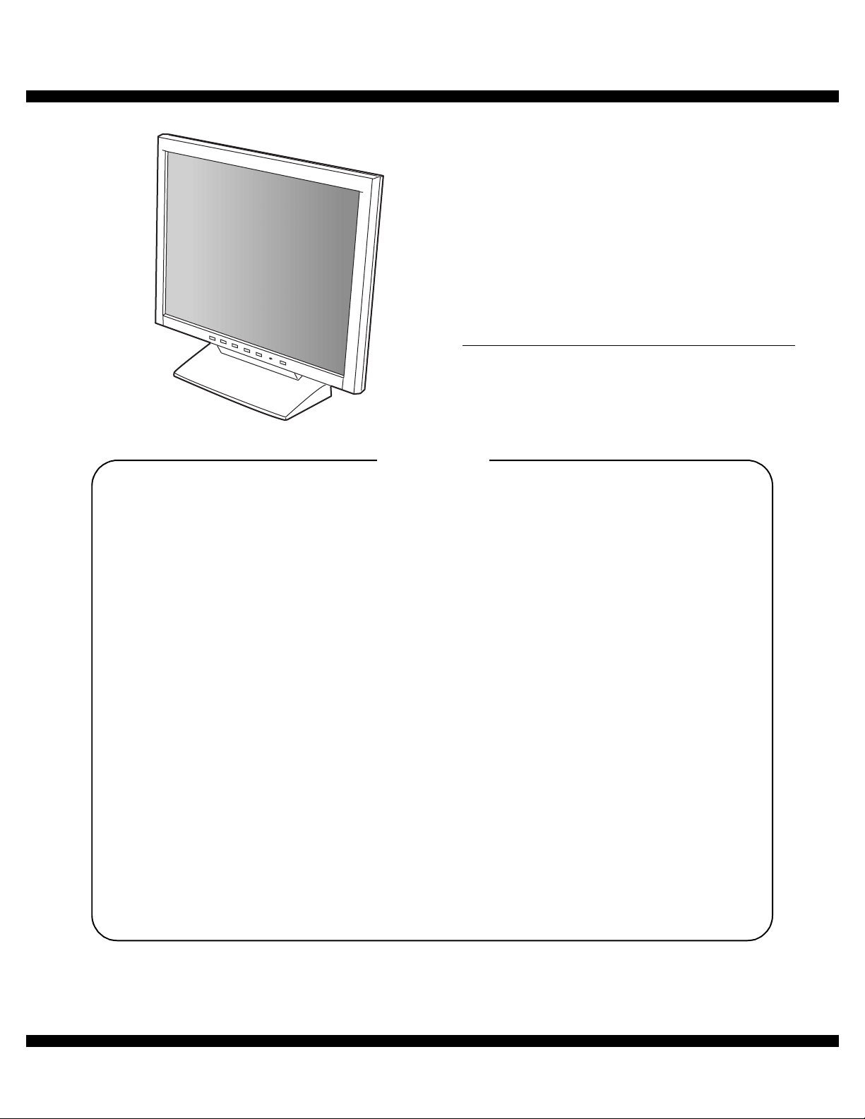
SERVICE MANUAL
MODEL
CONTENTS
CHAPTER 1. OUTLINE OF THE PRODUCT,
NOMENCLATURE AND FUNCTION. . . . . . . . . . . . . . . . . .1 - 1
CODE : 00Z
LLT15A3SME
LCD MONITOR
LL-T15A3
CHAPTER 2. CONNECTION, ADJUSTMENT,
OPERATION, AND FUNCTIONS. . . . . . . . . . . . . . . . . . . . .2 - 1
CHAPTER 3. DISASSEMBLY AND ASSEMBLY. . . . . . . . . . . . . . . . . . . .3 - 1
CHAPTER 4. TROUBLESHOOTING. . . . . . . . . . . . . . . . . . . . . . . . . . . . .4 - 1
CHAPTER 5. BLOCK DIAGRAM . . . . . . . . . . . . . . . . . . . . . . . . . . . . . . . .5 - 1
CHAPTER 6. CIRCUIT DIAGRAM. . . . . . . . . . . . . . . . . . . . . . . . . . . . . . .6 - 1
Parts marked with "!" are important for maintaining the safety of the set. Be sure to replace these parts with specified
ones for maintaining the safety and performance of the set.
SHARP CORPORATION
This document has been published to be used
for after sales servic e only.
The contents are subject to change without notice.
Page 2
CHAPTER 1. OUTLINE OF THE PRODUCT, NOMENCLATURE AND FUNCTION
1. SPECIFICATIONS
■
■ PRODUCT SPECIFICATIONS
■ ■
• Model name
LL-T15A3-H (Frosty gray) / LL-T15A3-B (Black)
• LCD display
38 cm measured diagonally
TFT LCD module
• Resolution (max.)
XGA 1024 x 768 pixels
• Displayable colors (max.)
Approx.16.19 million colors (6bit + FRC)
• Brightness (max.)
260cd/m
• Dot pitch
0.297 (H) x 0.297 (V) mm
• Contrast ratio
350:1
• Angle of visibility
Left-right 160°; Up-down 150° (contrast ratio u 5)
• Screen display size
Horizontal 304.1 mm x Vertical 228.1 mm
• Video signal
Analog RGB (0.7Vp-p) [75Ω]
• Sync signal
Separate Sync (TTL level: +/-)
• Expansion compensation
Digital screening (Enlargement VGA/SVGA etc. to full screen size.)
• Plug & Play
VESA DDC1/DDC2B compatible
• Power management
VESA: based on DPMS
• Input signal terminal
Mini D-sub 15 pin (3 row)
• Screen tilt
Upward approx.0 - 25°; downward approx.0 - 3°
• Power supply
AC100 - 240V, 50/60Hz
(Use special AC adapter, type NL-A53J of Sharp Corporation.)
• Temperature of operating environment
5 - 35°C
• Power consumption
Maximum 30W (Standby state: 3W) (Use special AC adapter.)
• Dimensions
343 (W) x 170 (D) x 308 (H) mm
• Weight
Approx. 3.4kg (approx. 2.5kg excluding stand)
(Excluding AC adapter.)
2
■
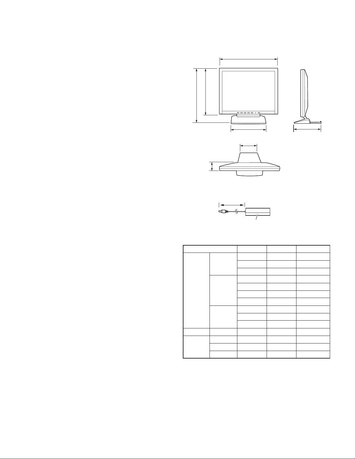
■ DIMENSIONS (UNITS: MM)
■ ■
343
267
308
200
130
44
Analog signal cable: Approx. 1.8m
Special AC adapter:
Approx. 1.8m
Approx. H 120mm x D 60mm x H 37mm
■
■ SIGNAL TIMINGS
■ ■
Display mode Hsync Vsync Dot frequency
VESA 640 x 480 31.5kHz 60Hz 25.175MHz
37.9kHz 72Hz 31.5MHz
37.5kHz 75Hz 31.5MHz
800 x 600 35.1kHz 56Hz 36.0MHz
37.9kHz 60Hz 40.0MHz
48.1kHz 72Hz 50.0MHz
46.9kHz 75Hz 49.5MHz
1024 x 768 48.4kHz 60Hz 65.0MHz
56.5kHz 70Hz 75.0MHz
60.0kHz 75Hz 78.75MHz
US text 720 x 400 31.5kHz 70Hz 28.3MHz
Power
Macintosh
series
• Recommended resolution is 1024 x 768.
• All are compliant only with non-interlaced.
• Frequencies for Power Macintosh are referenc e values. To connect,
another adapter (commercially available) may be required.
• If the monitor is receiving timing signals that are not compatible, [OUT
OF TIMING] will appear.
Follow your computer's instruction manual to set the timing so that it
is compatible with the monitor.
• If the monitor is not receiving any signal (synch signal), [NO SIGNAL]
will appear.
640 x 480 35.0kHz 66.7Hz 30.2MHz
832 x 624 49.7kHz 74.6Hz 57.3MHz
1024 x 768 60.2kHz 75Hz 80.0MHz
170
LL-T15A3 OUTLINE OF THE PRODUCT, NOMENCLATURE AND FUNCTION
1 – 1
Page 3
■
■ THE ANALOG RGB INPUT CONNECTOR PIN
■ ■
(Mini D-sub connector with 15 pins)
2. PRODUCT DESCRIPTION
12345
6789
11 12 13 14 15
No. Function No. Function
1 Red video signal input 9 DDC +5V
2 Green video signal input 10 N.C.
3 Blue video signal input 11 GND
4 N.C. 12 DDC data
5 N.C. 13 For Hsync signal input
6 For red video signal GND 14 For Vsync signal input
7 For green video signal GND 15 DDC clock
8 For blue video signal GND
■
■ POWER MANAGEMENT
■ ■
The monitor is based on VESA DPMS (Display Power Management Signaling).
To activate the monitor's Power Management function, both the video
card and the comp uter must conform to the VESA DPMS standard.
DPMS mode Screen
ON Display on 30W Yes Yes
STANDBY
SUSPEND Yes No
OFF No No
■
■ DDC (PLUG & PLAY)
■ ■
This monitor supports the VESA DDC (Display Data Channel) standard.
DDC is a signal standard for carry ing out Plug & Play functions on the
monitor or PC. It transfers information such as degree of resolution
between the monitor and PC. You can use this function if your PC is DDC
compliant and if it is set so that it can detect the Plug & Play monitor.
There are many va rieties of DDC due to the d ifferences between sys tems. This monitor works with DDC1 and DDC2B.
Display off 3W
10
Power
consumption
H-sync V-sync
No Y es
10
9
1 2 3 4 5 6 7 8
1. MENU button: This button is used to pop-up, select and close
the OSD (On Screen Display) Menu.
2. c button: This button is used to select menu options
when the OSD Menu is displayed.
3. e d buttons: When the OSD Menu is displayed:
These buttons are used to increase
or decrease the value of a selected option.
When the OSD Menu is not displayed:
These buttons are used to adjust backlight
brightness.
4. AUTO button: When the OSD Menu is displayed:
This button is used to turn off the OSD Menu.
When the OSD Menu is not displayed.
This button is used to perform automatic
adjustment of the screen (CLOCK, PHASE,
H-POS and V-POS).
5. Power LED: This LED is lit green when in use and orange
when in power-saving mode.
6. Power button: Pressing this button turns the power on. ( After
turning the power on, it may take a little time
before the screen displays.)
Press the button again to turn the power off.
7. Power terminal: The AC adapter is connected here.
8. Analog signal cable: Connects to the computer’s analog RGB out-
put terminal.
9. Security lock anchor: By connecting a security lock (commercially
available) to the security lock anchor, the monitor is fixed so that it cannot be transported.
The security slot works in conjunction with
Kensington Micro Saver Security Systems.
10. Ventilation open ings:
Note: Never block the ventilation openings as
this may lead to overheating inside the monitor
and result in malfunction.
LL-T15A3 OUTLINE OF THE PRODUCT, NOMENCLATURE AND FUNCTION
1 – 2
Page 4
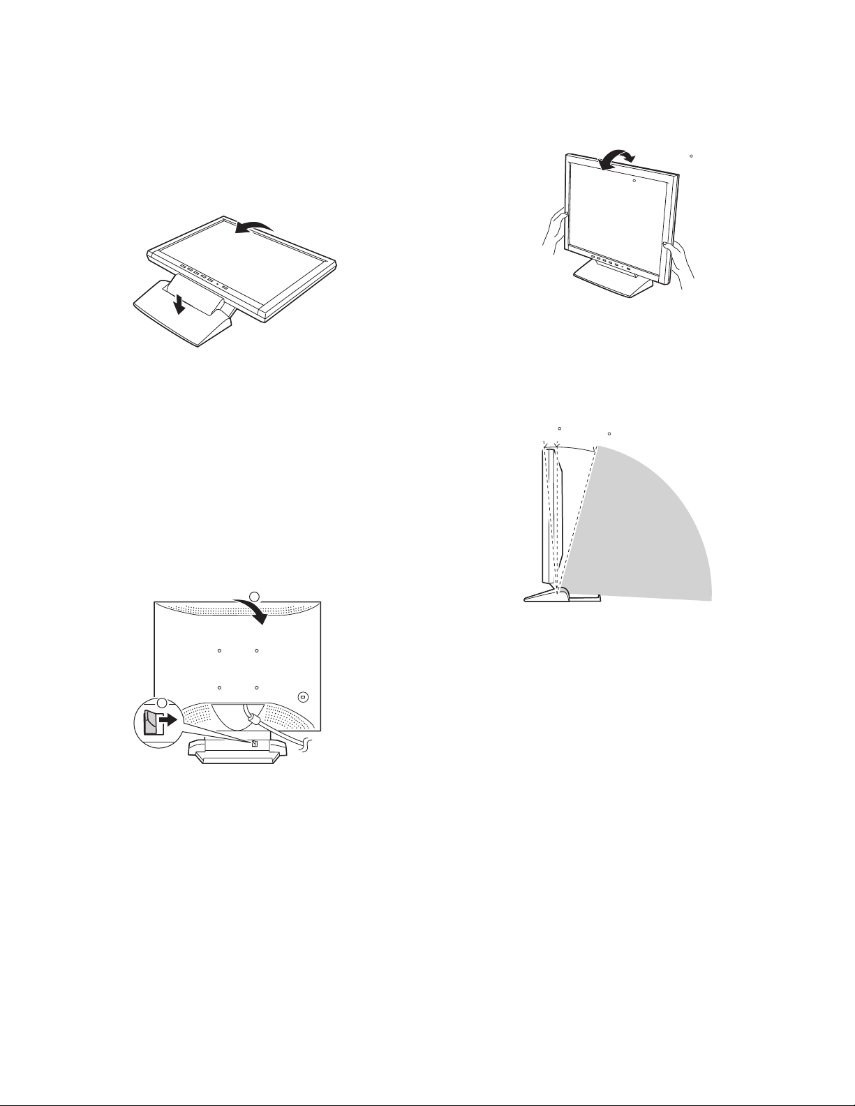
■
■ STANDING UP AND ADJUSTING THE MONITOR
■ ■
Caution:
• Pressure from hands on the LCD panel could cause damage.
• Be careful not to place any objects on the cables. Doing so may
result in disconnection.
1) Standing up the monitor
1. Press down on the stand and lift up the top section of the monitor.
2) Folding up the monitor (when packing it away)
• Except when folding away the monitor to transport it, do not fold down
the monitor.
Unnecessarily folding and unfolding the monitor could lead to malfunction.
1. Remove the AC adapter.
2. If carrying out adjustments to the monitor, place it upright.
3. While pressing the rear lock disable button 1, gently fold back the
monitor 2.
3) Angle adjustment
Lighty holding both sides of the monitor, adjust it to a suitable viewing
angle.
approx.25
approx.3
• Do not use the monitor when tilted back beyond approxim ately 25°.
The monitor may fall over leading to injury or malfunction.
approx.3
approx.25
Prohibited range
2
1
LL-T15A3 OUTLINE OF THE PRODUCT, NOMENCLATURE AND FUNCTION
1 – 3
Page 5
CHAPTER 2. CONNECTION, ADJUSTMENT, OPERATION, AND FUNCTIONS
1. CONNECTING THE MONITOR AND TURNING THE MONITOR ON AND OFF
Caution:
• When connecting, ensure that both the monitor and computer are
switched off.
• Be careful not to overly bend the cable or add extension cords as
this could lead to a malfunction.
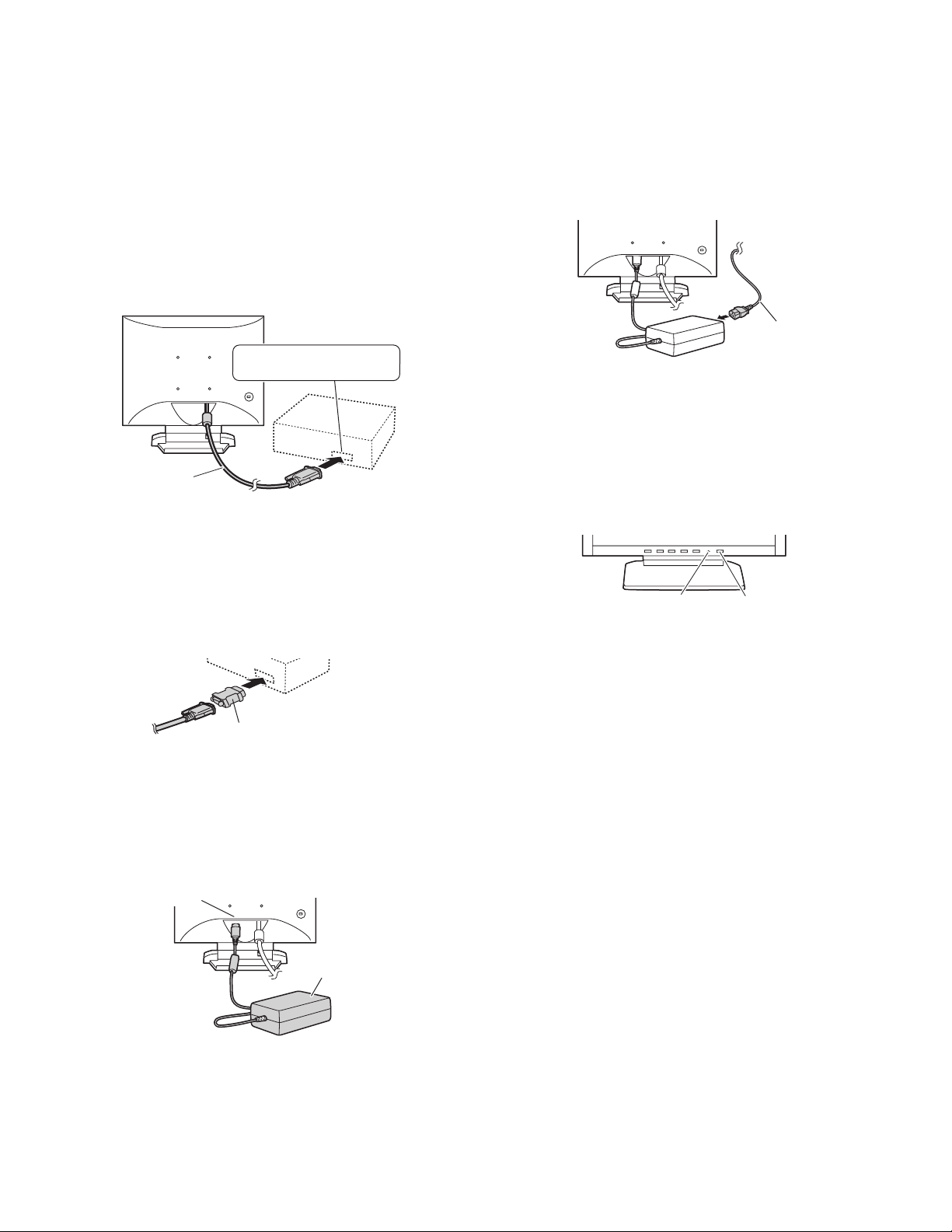
1-1. CONNECTING THE MONITOR TO A COMPUTER
Analog RGB output terminal
(Mini D-sub 15 pin, 3 row)
Analog signal cable
• Paying attention to connector direction, firmly inse rt the signal cable
to terminal, and then tighten the screws at both sides.
If connecting to a D-sub 15 pin 2 row Apple Power Macintosh, attach a
Macintosh conversion adapter (commercially available) to the analog
signal cable.
Macintosh conversion adapter
2. Attach the power cord to the AC adapter and place the power plug
into the AC outlet.
AC outlet
Power cord
1-3. TURNING THE POWER ON
1. Press the monitor's POWER button.
2. Turn on the computer.
The power LED will be lit green, and the screen will display an
image.
Power LED Power button
Note:
• If us ing the monitor for the first time or after having changed the
system settings during use, perform an automatic screen adjustment.
• Depending on the computer or OS, it may be necessary to use the
computer to install monitor set-up information. If so, follow the
steps below to install the monitor set-up information.
1-2. CONNECTING THE MONITOR TO A POWER
SOURCE
1. Connect the AC adapter to the monitor's power terminal.
Power terminal
AC adapter
LL-T15A3 CONNECTION, ADJUSTMENT, OPERATION, AND FUNCTIONS
1-4. TURNING THE POWER OFF
1. Turn the computer off.
2. Press the monitor's POWER button.
The Power LED will disappear.
If the monitor is not going to be used for a long period of time, be
sure to unplug it from the AC outlet.
2 – 1
Page 6
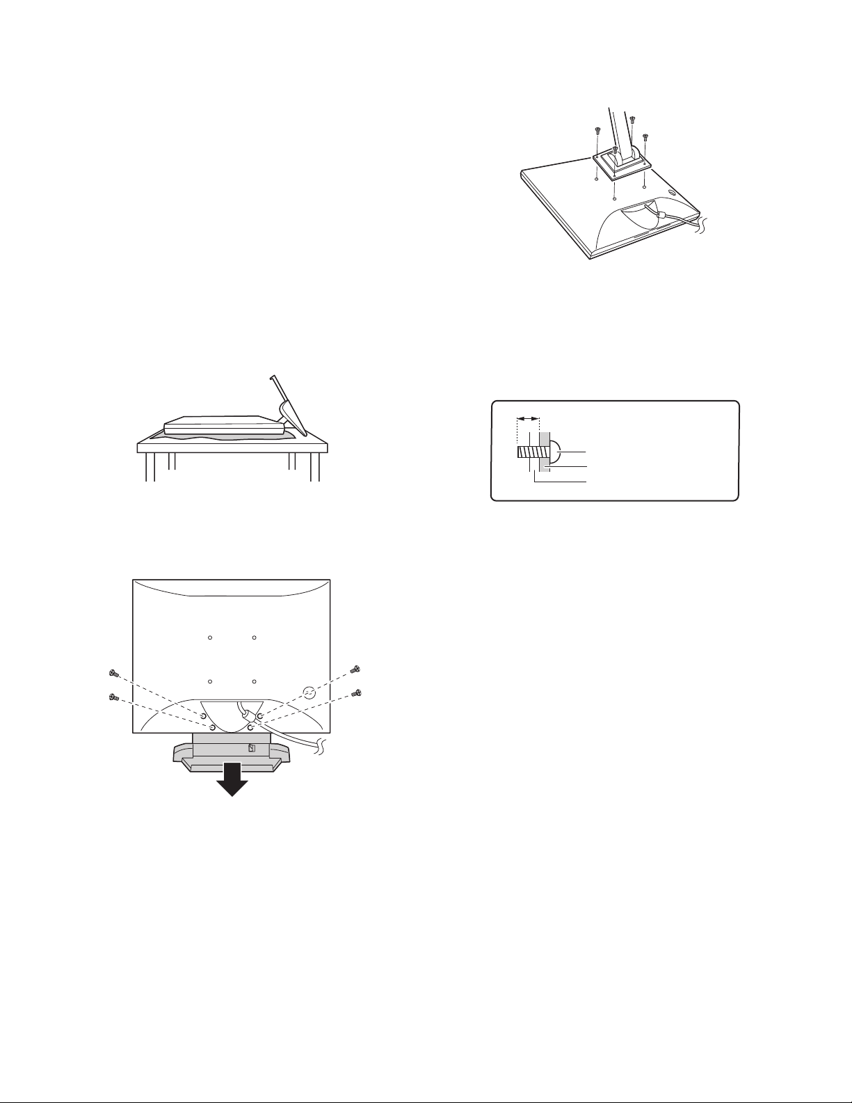
1-5. INSTRUCTIONS FOR ATTACHING A VESA COMPLIANT ARM
An arm or stand based on the VESA standard (comme rcially available)
can be attached to the monitor.
Procurement of the arm or stand is at the customer's discretion.
When choosing the arm to be installed please take note of the following
points.
• The arm should be compatible with the VESA standard, and there
must be a gap of 75mm x 75mm between the screw holes on the
section to be attached.
• The arm m ust not fall off or break off after being attached to the
monitor.
Note: Do not overly bend the cable or add extension cords as this
could lead to malfunction.
1. Turn off the power switch and remove the AC adapter from the
monitor's power terminal.
2. Being careful not to damage the monitor, spread out a soft cloth and
lay the monitor on it display-side down.
4. Attach the arm to the monitor with four screws.
Note: The screws used to attach the arm should be M4 screws with a
length of 4 mm ~ 6 mm protruding from the surface to be
attached. Using different screws could lead to malfunction or
may lead to the monitor falling off, internal damaged, personal
injuly.
4 ~ 6mm
Screw used to attach arm
Arm
Part of monitor to which
arm is attached
3. Remove the four screws and then remove the stand from the monitor.
Note:
• The stand is specially made for use with this monitor. Once having
removed the stand, never attempt to attach it to another device.
• Once having removed the screws, store them together with the
stand and if the stand is ever re-attached be sure to use the original
screws.
Using different screws could lead to malfunction.
5. Connect the AC adapter to the monitor's power terminal.
LL-T15A3 CONNECTION, ADJUSTMENT, OPERATION, AND FUNCTIONS
2 – 2
Page 7

2. ADJUSTMENT
MENU
MENU
2-1. ADJUSTMENT METHOD
1) Resetting all adjustment values
Power ON
Press the above two buttons at same time, and while turn the power on.
2) Adjustment lock function
Power ON
While pressing the MENU button, turn the power on.
3) Adjusting the backlight
buttons
4) Screen adjustment
MENU
ADJUSTMENT
AUTO
CLOCK
PHASE
H-POS
V-POS
buttons
buttons
buttons
buttons
MENU
GAIN CONTROL
AUTO
MENU
WHITE BALANCE
MENU
MODE SELECT
MENU
END
5) Version display (for service)
eSELECT d
Display the software version.
6) Aging (for service)
MENU SELECT e
Each color is displayed in order automatically.
When the test is terminate, Power off.
(COOL STD
Power ON
Power ON
BLACK LEVEL
CONTRAST
DISPLAY COLORS
WARM USER)
OSD H-POSITION
OSD V-POSITION
400 LINES
SCALING
buttons
buttons
buttons
buttons
CONTRAST
(R/G/B)
R-CONTRAST
G-CONTRAST
B-CONTRAST
buttons
buttons
buttons
buttons
buttons
buttons
buttons
LL-T15A3 CONNECTION, ADJUSTMENT, OPERATION, AND FUNCTIONS
2 – 3
Page 8

2-2. ADJUSTMENT ITEM LIST
BUTTON ITEM ADJUSTMENT DESCRIPTION
MENU MENU 1:
ADJUSTMENT
MENU 2:
GAIN CONTROL
MENU 1
4
MENU 2
4
MENU 3
MENU 3:
WHITE BALANCE
4
MENU 4
4
MENU END
MENU 4:
MODE SELECT
c
e d
POWER OFF
MANUAL CLOCK 0~255 CLOCK:Adjust so that vertical flicker noise is not emit-
ted. (e d buttons)
PHASE 0~63 PHASE: Adjust so that horizontal flicker noise is not
H-POS 0~255
V-POS 0~31
emitted. (e d
H-POS (horizontal positioning) and
V-POS (vertical pos it ioning)
To center the screen image within the boundaries of
e d buttons)
e de d
the screen, adjust the left-right (H- POS) values and
the up-down (V-POS) values. (e d
AUTO Automatic screen adjustment
Options in the ADJUSTMENT Menu can be adjusted
automatically
(CLOCK, PHASE, H-POS V-POS).
MANUAL BLACK LEVEL 0~63
BLACK LEVEL: Total screen brightness can be adjusted
while watching the color pattern.
e d
buttons)
(
CONTRAST 0~63 CONTRAST: While watching the color pattern,
adjustments can be made so that all
graduations appear. (e d
DISPLAY
COLOS
260K (260,000),
16M (16.19 million)
Maximum display colors can be set. (e d
AUTO GAIN CONTROL Menu
AUTO:Every menu option is automatically adjusted
using the Auto Gain Control function.
COOL • STD • WARM
(5 levels),
USER R • G • B: 0~63
WHITE BALANCE Menu
COOL : Color tone bluer than standard
• : Color tone slightly bluer than standard
STD : Color tone standard setting
• : Color tone slightly redder than standard
WARM : Color tone redder than standard
USER
R-CONTRAST: e button for blue-green
d button for red
G-CONTRAST: e button for purple
d button for green
B-CONTRAST: e button for yellow
d button for blue
OSD H-POSITION
(OSD horizontal position)
OSD V-POSITION
(OSD vertical position)
The position of the OSD display can be moved to the
left and right. (e d buttons)
The position of the OSD displa y can be moved up an d
down. (e d buttons)
400 LINES 640, 720 You can specify the horizonal resolution of a 400 line
screen when using US text, etc. (e dbuttons)
SCALING
(Level of scaling)
LEVEL1, LEVEL2 SCALING (Level of scaling)
Adjusts the image to optimum sharpness when Screen
expansion is taken. (e dbuttons)
Select the item
Bright: 0~31 Adjusting the backlight
e d buttons)
e de d
e d buttons)
e de d
e d buttons)
e de d
LL-T15A3 CONNECTION, ADJUSTMENT, OPERATION, AND FUNCTIONS
2 – 4
Page 9

CHAPTER 3. DISASSEMBLY AND ASSEMBLY
1. Remove the screws and then remove the stand unit.
2. Remove the front panel.
4. Remove the screws. Remove the connector locking seat and then
remove the connectors.
5. Remove the inverter board and key board f rom the LC D modul e.
6. Remove the screws and then remove the shield.
3. Remove the screws and connectors, and then remove the LCD unit.
7. Remove the screws and connectors, and then remove the I/F board.
LL-T15A3 DISASSEMBLY AND ASSEMBLY
3 – 1
Page 10

CHAPTER 4. TROUBLESHOOTING
No power supply
Does LED turns on in green
when power switch is turned
on?
Yes
Backlight turns ON?
Yes
Check for RGB cable input
signal.
A
Normal
Replace RGB cable.
Defective
No
No
Check each pin terminal
of JP5.
Defective
LED turns on in orange?
Normal
No
Yes
Check whether the unit is in power save
mode (synchronizing signal is not input.).
1) PC is turned off?
2) RGB cable is disconnected?
3) Synchronizing signal is output from RGB
cable?
No
Synchronizing signal is input to main PWB?
Yes
No
Check inverter PWB unit.
*
Note: Use caution when checking output
Check output circuit to JP5.
1) If +12V is NG, replace main
PWB.
Replace LCD module lamp with
a new one.
side because it has a high voltage.
(1400 Vrms when starting)
Normal
Defective
Replace inverter PWB
unit with a new one.
LL-T15A3 TROUBLESHOOTING
Replace RGB cable
with a new one.
Check power input system.
1) AC adapter
* Normal?
* Connected properly?
2) Blown out fuse (F1) on main PWB?
3) EEPROM (U11) has +5V (VCC)?
4) LED
* Check LED for breakage.
* Check the path between J5 (5pin)
and U11 (27pin) or J5 (6pin) and U11
(26pin).
* Check the cable for disconnection.
5) Check connector of power jack PWB
for breakage. Check the cable for
disconnection.
Yes
Replace any defective unit.
[ 1) Adapter, 2) A Main PWB, 3) Switch
PWB, 4) Power jack PWB] with a new one.
4 – 1
Page 11

Screen does not operate normally.
Check screen condition by changing display modes.
Reset the microprocessor to check if screen condition changes.
(Press and hold MENU and SELECT buttons while turning on power switch.)
A
Screen stays in black. Screen stays in white.
Check RGB cable.
Screen jitters or on-screen
characters flicker.
Defective
Replace RGB cable with
a new one.
Abnormal color
Check the following signals
1) Check if module control signal is output.
2) J6 Nos. 57, 58, 59 and 60 pins signal
outputs show DC+5V?
Check the LCD control signal and
microprocessor control circuits around U1, X1,
U11, U8 and U9.
Yes No
Main PWB defective.
CLOCK and PHASE
can be adjusted?
Yes No
Switch PWB defective.
Does abnormal area move on
screen when BLACK LEVEL or
CONT is changed after H-POS
or V-POS is set?
Yes No
LCD panel defective.
Cable defective.
LL-T15A3 TROUBLESHOOTING
4 – 2
Page 12

CHAPTER 5. BLOCK DIAGRAM
1. BLOCK DIAGRAM
■■■■ GENERAL
LAMP
TFT LCD PANEL
LAMP
INTERFACE
UNIT
DC
JACK
UNIT
INVERTER
■■■■ INTERFACE UNIT
SIGNAL CABLE
DB15
RGB,H/V
INPUT
12 PIN RGB I/P
EDID
24LC21
Protective
J1
OVER VOLTAGE
PROTECTION
ESD
Circuit
OSC
20MHZ
MCU
EEPPROM
KEY-SWITCH UNIT
OSC
50MHz
SCALING
gmZAN2
Jump
AC 100V
INPUT
J6
JP5
J5
AC
ADAPTER
CONNCTOR
60PIN
OSD CONTROLINVERTER
TFT-LCD
Panel
LAMP
OSD Control BD
POWER JACK
BD
Power
JP6
TL 494
5V TO 3.3V
Regulator
5V TO 2.5V
Regulator
LL-T15G3 BLOCK DIAGRAM
5 – 1
PMOS
To Panel
(J6)
To Scaler
To Scaler
Page 13

2. CONNECTOR SIGNAL TABLE
1
1 LCD SIGNAL INPUT
11
J9
Used connector : AMP 6240-36
Pin No. Symbol Function
1GNDGND
2NC
3NC
4NC
5GNDGND
6GNDGND
7NC
8NC
9 RO0 RED even pixel
10 RO1 RED
11 GND GND
12 RO2 RED
13 RO3 RED
14 RO4 RED
15 RO5 RED (MSB)
16 GND GND
17 NC
18 NC
19 GO0
20 GO1 GREEN
21 GND GND
22 GO2 GREEN
23 GO3 GREEN
24 GO4 GREEN
25 GO5 GREEN (MSB)
26 GND GND
27 NC
28 NC
29 BO0 BLUE even pixel
30 BO1 BLUE
31 GND GND
32 BO2 BLUE
33 BO3 BLUE
34 BO4 BLUE
35 BO5 BLUE (MSB)
36 GND GND
data signal (LSB)
GREEN even pixel
data signal (LSB)
data signal (LSB)
J8
Used connector : FAMP 6240-40
Pin No. Symbol Function
1GNDGND
2 VDD +5V power
3 VDD +5V power
4NC
5NC
6 RE0 RED odd pixel
data signal (LSB)
7 RE1 RED
8GND
9 RE2 RED
10 RE3 RED
11 RE4 RED
12 RE5 RED (MSB)
13 GND
14 NC
15 NC
16 GE0 GREEN odd pixel
data signal (LSB)
17 GE1 GREEN
18 GND GND
19 GE2 GREEN
20 GE3 GREEN
21 GE4 GREEN
22 GE5 GREE N (MSB)
23 GND GND
24 NC
25 NC
26 BE0 BLUE odd pixel
data signal (LSB)
27 BE1 BLUE
28 GND GND
29 BE2 BLUE
30 BE3 BLUE
31 BE4 BLUE
32 BE5 BLUE (MSB)
33 GND GND
34 NC
35 NC
36 NC
37 ENAB Data enable
signal
38 GND GND
39 DCLK LCD_CLK
40 GND GND
2
2 JP5 (TO INVERTER TERMINAL)
22
Used connector : FPH_5
Pin No. Symbol Function
1 ON/OFF HIGH=ON,
2GNDGND
3 BRT_RANGE Brightness
4GNDGND
5 +12V +12V IN
3
3 JP1(TO DC JACK BD)
33
Used connector : F4_HEADER
Pin No. Symbol Function
1 +12V +12V IN
2 +12V +12V IN
3GNDGND
GND GND
4
4 J1 (Signal Input Terminal)
44
Used connector : FPH_12P
Pin No. Symbol Function
1 SCL DDC
2 SDA DDC
3 DDC +5V DDC
4 V-SYNC V-SYNC
5 H-SYNC H-SYNC
6GNDGND
7 BLUE BLUE
8GNDGND
9 GREEN GREEN
10 GND GND
11 RED RED
12 GND GND
5
5 J5 (TO KEY SW BD)
55
Used connector : FHEADER_9
Pin No. Symbol Function
1 KEY SELECT SELECT
2KEY DOWN<
3KEY UP>
4 KEY MENU MENU
5 LED GREEN LED GREEN
6 LED RED LED RED
7GNDGND
8 KEY POWER POWER
9 KEY AUTO AUTO
LOW=OFF +5V
control of inverter
+5V
LL-T15A3 BLOCK DIAGRAM
5 – 2
Page 14

1/4
12345678
12345678
12345678
12345678
+3.3V
B2 220Z/1 00M
+3.3V
TP2
C200
+5V
DDC+5V
33P
C162
C161
15P_NA
15P_NA
C160
CHAPTER 6. CIRCUIT DIAGRAM
D
D
D
D
DIGITAL
SUPPLY
DECOUPLING
B5
220Z/100M
DVDDA
C3
0.1uF
C2
0.1uF
C1
22uF/16V
Head Sink Fix Hole
1
RD100
1uF
R1
10K
HS_VGA
DDC_SCL
DDC_SDA
VS_VGA
DDC+5V
B6 12 0z/100M
B7 12 0z/100M
B4 12 0z/100M
B3 12 0z/100M
123456789
J1
D
D
D
D
+3.3V+2.5V
VCC_3.3V
SVDDA
B8 220Z/1 00M
C4
+
0.1uF
B89 120z/100M
B
B
B
C
C
C
C
O_R2 4
O_R4 4
O_R3 4
E_B2 4
E_B3 4
E_B4 4
E_B6 4
E_B7 4
E_G3 4
E_G6 4
E_G4 4
E_G5 4
E_G7 4
E_B4
E_B2
E_B3
E_G3
E_G7
E_G4
E_G6
E_G5
81
81
72
63
54
72
63
54
RP3 33
RP4 33
PD7BLUE-
PD10
PD8
PD13
PD14
PD11
PD9
PD12
57
626364656667686970
PD8
PD7
PD9
PD14
PD13
PD12
PD11
PD10
RESERVED
RESERVED
RESERVED
BLUE-
234
83
86
C47
0.01uF
C46
0.01uF
C45
0.01uF
U2C
74F14
SO14
56
U2B
74F14
SO14
34
HSYNC
BAV99LT1
D6
C173
NC
R6 100
NC
510
R140
HS_VGA
E_B5 4
E_B5
O_R4
E_B6
O_R2
E_B7
O_R3
O_R5
63
54
81
81
72
63
54
RP6 33
RP5 33
PD19
PD15
PD17
PD21
PD16
PD18
PD20
39
42
4647484950515253545556
PD20
PD19
PD18
PD17
PD16
PD15
U1
N/C
RESERVED
RESERVED
RESERVED
RESERVED
97
130
135
145
152
156
R12
100
R11
100
R10
100
U2D
147
U2E
147
BAV99LT1
E_G2 4
E_R7 4
E_R5 4
E_R6 4
E_R3 4
E_R4 4
E_R2 4
E_R2
E_R3
E_R5
E_R4
E_G2
E_R7
E_R6
220Z/100M
B86
B85
220Z/100M
FOR ZAN2 FOR ZAN1
C13
0.1uF
C12
0.1uF
C11
0.1uF
C10
0.1uF
C15
0.1uF
C9
0.1uF
C8
10V
22uF/16V
C38
0.1uF
RVDDA
C7
0.1uF
C6
0.1uF
C20
C19
C5
22uF/16V
B10 220Z/1 00M
C18
R_IN
C17
10P
B9 100
10p
C16
BAV99LT1
D2
10uF/16V
75 B84
R2
C163
VGA_R
B91 120z/100M
B90 120z/100M
101112
PH_12P
C28
0.1uF
C26
0.1uF
C25
0.1uF
C24
0.1uF
C23
0.1uF
10V
C22
0.1uF
22uF/16V
C21
22uF/16V
220Z/100M
C37
0.1uF
VDDA
C35
0.1uF
C34
0.1uF
C33
0.1uF
C32
0.1uF C185
1uF
1000P
0.1uF
C31
22uF/16V
B12
220Z/100M
G_IN
C30
10P
B11 100
10p
C29
BAV99LT1
D3
75
R3
VGA_G
TO EXTERNAL SIGNAL CABLE
OPEN FOR ZAN1,SHORT FOR ZAN2
R141 0
60
INPUT AC
C41
C40
D4
R4
40
12
149
108
58
11
139
125
77
79
129
136
137
143
84
88
92
96
COUPLING
RED+
C42 0.01uF
10P
10p
75
+5V
RVDD3
CVDD1
RVDD2
RVDD1
CVDD4
CVDD2
SVDD
DVDD
GREEN+
C43 0.01uF
R50NC0603
12
R49NC0603
12
C
C
C
C
SYN_VDD
SRVDD2
SRVDD1
ADC_VDD2
ADC_VDD1
ADC_VDDA
C44 0.01uF
10V
ANALOG SUPPLY
DECOUPLING
B_IN
B13 100
BAV99LT1
VGA_B
63
54
81
72
63
54
RP2 33
RP1 33
PD2
PD3
PD4
PD1
PD5
PD0
71
PD4
PD3
PD2
PD1
PD0
RESERVED_3.3V
PLL_DVDDA
PLL_SVDDA
DAC_SVDDA
PLL_RVDDA
ADC_BVDDA
ADC_GVDDA
ADC_RVDDA
BLUE+
GREEN+
RED+
87
91
94
95
RED-
BLUE+
+5V
V_STATE 3
R8 NC
VSYNC
D5
R5 100
NC
510
R139
VS_VGA
72
PD6
PD6
PD5
GREEN-
RED-
90
GREEN-
147
147
B
O_B2 4
O_G2 4
O_G3 4
O_G6 4
O_G4 4
O_G5 4
O_G7 4
O_R6 4
O_R5 4
O_R7 4
O_R6
O_R7
O_G2
O_G3
O_G5
O_G4
O_B2
O_G7
O_G6
72
63
54
81
72
63
54
81
72
RP8 33
RP7 33
PD27
PD28
PD26
PD24
PD22
PD29
PD30
PD25
PD23
293031
32333435363738
PD30
PD29
PD28
PD27
PD26
PD25
PD24
PD23
PD22
PD21
TCLK
XTAL/RESERVED
VSYNC
HSYNC/CS
STI_TM1
RESERVED
STI_TM2
141
142
148
150
153
154
X1
74F14
SO14
98
B83 220Z/1 00M
+3.3V
74F14
SO14
11 10
B
B
B
B
O_B3 4
O_B4 4
O_B6 4
O_B7 4
O_B5 4
O_B3
O_B7
O_B4
O_B6
O_B5
81
81
72
63
54
RP10 33
PD34
PD31
PD35
PD33
PD32
202122232425262728
PD37
PD36
PD35
PD34
PD33
PD32
PD31
gmZAN2
PSCAN
OSD_HREF
SCAN_IN1
SCAN_IN2
SCAN_OUT1
SCAN_OUT2
115
116
155
157
159
160
C49
22P
R20 33
5
4
OUT
GND
VDD
E/D
OSC50MHz
8
1
C165
0.1uF
PD40
PD39
PD38
OSD_VREF
OSD_CLK
OSD_DATA0
117
118
119
10
13141516171819
PD44
PD43
PD42
PD41
OSD_DATA1
OSD_DATA2
OSD_DATA3
OSD_FSW
120
121
122
+5VDDC+5V
LCD_CLK 4
B14 5.6ohm
R35 0.1 uF
beat noise solution
6
789
PD47
PD46
PD45
PCLKA
HFS
HDATA
RESETn
IRQ
HCLK
98
99
100
101
103
HFS3
HCLK3
RESET#3
HDATA03
VCC_FROM_PC
D1
BAV70LT1
B1
500z/100M
B16 120z/100M
434445
PCLKB
113
DE 4
PDISPE
MFB0
112
R36 22
737475
PVS
PHS
MFB1
MFB2
MFB3
111
110
C57
R40 NA
76
MFB4
109
107
+5V
33P
R55
R54
EN_LCD 3
R43 NA
PPWR
MFB5
106
R44 10 K
47K
47K
EN_BL# 3,4
PBIAS
MFB6
105
U5 24C21
MFB7
MFB8
102
104
R45 NA
C190
C64
81234
VCC
765
R56 100
VSYNC
MFB9
MFB10
123
124
R46 10 K
NC
TEST
VCLK
SCL
R57 100
R58 100
DDC_SCL
DDC_SDA
MFB11
WP
SDA
1uF
0.1uF
VSS
C66
C65
A
RESERVED_CVSS1A
SRVSS2
SYN_VSS
SVSS
DVSS
CVSS4
RESERVED_VSS
CVSS3
RVSS4
RVSS3
CVSS2
RVSS2
SRVSS1
RVSS1
CVSS1
RESERVED_CVSS2A
SUB_RGNDA
SUB_DGNDA
SUB_SGNDA
PLL_RGNDA
DAC_SGNDA
PLL_SGNDA
PLL_DGNDA
DAC_DGNDA DAC_DVDDA
ADC_GND2
ADC_GND1
SUB_GNDA
ADC_GNDA
ADC_BGNDA
ADC_GGNDA
ADC_RGNDA
HDATA13
HDATA23
HDATA33
47P
47P
A A
A A
A A
A
OPEN FOR ZAN1,SHORT FOR ZAN2
5
158
151
140
126
114
147
72
61
41
1
59
146
132
133
144
138
134
131
127 128
78
80
81
82
85
89
93
21
21
21
21
3
3
3
3
87654
87654
87654
87654
LL-T15A3 CIRCUIT DIAGRAM
6 – 1
Page 15

B
B
B
123456789
AK
AK
AK
AK
AK
B25
B28
B31
B30
B29
B24
B27
B26
KEY_SELECT#
LED_RED
IRQ
LED_GREEN
KEY_DOWN#
KEY_UP#
KEY_MENU#
RP12
RP11
+5V
B
HEADER_9
TO KEY SW BD
AK
B32
C92
33P
C91
33P
C90
33P
C89
33P
C88
33P
C87
33P
C86
33P
HOT_KEY
+5V
R152
4.7K
R148
4.7K
4.7K*4
4.7K*4
C94
0.1uF
123
45
A0A1A2
VSSSI
U10
SCKWPVCC
678
R84
10K
R83
10K
SCL
SDA
+5V
RP15
4.7K*4
RP14
4.7K*4
B
B
B
B
54
63
72
81
54
63
72
81
24LC16B
PARAMETER
EEPROM
R145
4.7K
81
72
63
54
81
72
63
54
Q8
EC
+5V
B
R87
EN_BL# 2,4
EN_LCD 2
EN_BL#
EN_LCD
LED_AMBER#
242526272829303132
A8/P2.0
A9/P2.1
U11
P1.0/T2
P1.1/T2EX
2345678
HDATA02
HDATA12
MMBT3906L
15K
KEY_MENU#
A10/P2.2
A11/P2.3
P1.2/ECI
P1.3/CEX0
R127 22
HDATA22
HDATA32
R88 470
KEY_UP#
KEY_SELECT#
A12/P2.4
A13/P2.5
A14/P2.6
P1.4/CEX1
P1.5/CEX2
P1.6/CEX3/WAIT#
AUDIO_PWR
HFS2
HCLK2
B94
A_PWR
LED_RED
+5V
KEY_DOWN#
3335363738394041424344
PSEN#
A15/P2.7
ALE/PROG#
P1.7/CEX4/A17/W
RST
P3.0/RXD
9
1011131415161718192021
RESET
BRI_PWM4
300z/100M-NC
D
D
D
D
C79
470uF/16V
2/4
12345678
12345678
12345678
12345678
+3.3V
+5V
CORE_7X13X2SA
12VIN
CHOKE1
POWER CONN. 5V-->3.3V
+
C78
10uF/16V
CPWX4.3
+
1uF
0805
C80
16V
R70
220
0603
1%
R67
130
0603
1%
2
4
VOUT0
VOUT1
EZ1084CT
VIN
GND
U7
3
1
C77
10uF/16V
CPWX4.3
+
C208
0.1uF
AK
RLZ5.1
+
C75
470uF/16V
R91 0
R155 0.18_NC 1W
+
C202
470uF/16V
L1 57UH/2.5A
COM_CHOKE_4A
F1 RGE300
JP1
R154
10
C201
222
D17
SR34
C209
0.1uF/NC
678
CEM9435
U13
123
45
C207
0.1uF/NC
CBE
AK
Q14
MMBT3904L
D18
0.1uF D16
0805
470uF/16V
23
14
TO DC JACK BD
4_HEADER
D
D
D
D
1N4148
123
1K
R153
C206
C71
1uF
C69
+
C179
0.1uF
C70
0.1uF
4
+3.3V
+5V
R156 3.6K
IN1+
15
REF OUT
1413121110
B88
B87
500z/100M
R1574.7K
R158 1M
316
2
IN1OC
R163
220
500z/100M_NC
C205
C204
4
FBK
DTC
VCCC2E2
K
104
R159
510
102
5
CT
C211
D19
RLZ5.1
R164
220
LCD POWER
PANEL VDD SELECTOR
C83
10uF/16V
CPWX4.3
+
C84
0.1U/20V/NA
7.5K
R160
7
RT
GND
16
16 15
E1
C1
U14
AP494
9
8
0.1uF
A
C
C
C
C
J7
123456789
C195
1uF
VCC_LCD
+5V
R161 3.6K
0805
678
DRAIN1
DRAIN2
DRAIN3
FDS4435
SOURCE1
SOURCE2
SOURCE3
GATE DRAIN
U8
123
45
LOW ON
R77
10K
EC
Q6
B
MMBT3906L
R78 47K
LOW ON
EN_LCD
C194
0.01uF
C193
1uF
0805
C188
10V
+2.5V
+5V
R79
+5V
RESET
C
C
C
C
22uF/16V
R150
120
2
U12
VOUT
GND
1
VIN
AMS1117_2.5V
3
C187
0.1uF
C186
10V
22uF/16V
C192
1uF
0805
C191
10uF/16V
CPWX4.3
+
RESET
Q7
4.7K
MMBT3904L
CBE
R82 470K
R81
D13
+5V
C93
0.1uF
+5V
R80
470
D211N4148
D231N4148
D221N4148
D201N4148
R151
120
RESET# 2
100K/NA
47K
R85
1N4148/NA
AK
C95
312
GND
OUT
VCC
U9
HEADER_9-NC
J5
USE 9PR150 R151 ARE 100 OHM FOR ADJUSTABLE
D251N4148
D261N4148
300z/100M
10uf/16V
KIA7042
HOT_KEY
AUTO_BRI_DETECTAUTO_BRI_CTRL
AD7/P0.7
AD6/P0.6
AD5/P0.5
P3.1/TXD
P3.2/INT0#
P3.3/INT1#
P3.4/T0
IRQ
B95
Q13
EC
B
R149
SDA
SCL
AD4/P0.4
AD3/P0.3
AD2/P0.2
AD1/P0.1
P3.5/T1
P3.6/WR#
P3.7/RD#/A16
XTAL2
C96 22P
AUDIO_PWM
+5V
V_STATE2
300z/100M-NC
A_PWM
A
LED_GREEN
MMBT3906L
R93 47 0
15K
+5V
B33 220 z/100M
VCC
EA#/VPP
AD0/P0.0
NIC
NIC
XTAL1
VSS
1
22
122334
Y2
20MHz/22P
R53
1M
C97 22P
Q10
AUTO_BRI_CTRL
CBE
R92
AUTO_BRI_DETECT
220Z/100M-NC 0805C
B35 300z/100M-NC
B34
B36 300z/100M-NC
1234567
1234567
JP6
A A
A A
A A
A
C99
C98
NIC
NIC
MMBT3904L-NC
10K-NC
+5V
A_PWM
A_PWR
B37 220Z/100M-NC
21
21
21
21
3
3
3
3
22uF/16V
0.1uF
M6759
1234 FOR SENSOR
5678 FOR AUDIO
B96 220Z/100M-NC0805C
8
87654
87654
87654
87654
8
HDR/MA/8PX1
JST
B8P-VH
LL-T15A3 CIRCUIT DIAGRAM
6 – 2
Page 16

B
B
B
D
D
D
D
3/4
12345678
12345678
12345678
12345678
DCLK
12345678910111213141516171819
J8
123456789
VDD
J9
123456789
DCLK
R97 120z/100MHz
LCD_CLK2
DUE TO ODD & EVEN ARE ERROR NAMING
SO PANEL NAME IS OPPOSITE.
C117
47P
C116
47P
C115
47P
C114
47P
C113
47P
C112
47P
C111
47P
C110
47P
C109
47P
C108
47P
C107
47P
C106
47P
C105
47P
C104
47P
C103
47P
C102
47P
C101
47P
C100
47P
BE5
BE0
BE2
BE1
BE4
BO3
820k
RE0
BO2
RE1
BO1
R? 1M
+3.3V
BE3
1011121314151617181920 21
RE2
RE5
RE3
RE4
GE1
GE0
GO5
GO2
GO3
GO4
BO0
101112131415161718 19
RO0
RO2
RO5
RO3
RO4
RO1
1M
C122
ENAB
VDD
BO4
BO5
1234567891011121314151617
R146
beat noise solution
RE2
RE3
RE4
RE5
GE2
GE0
GE1
GE3
GE4
RE0
RE1
GO1
GE4
GE5
22232425262728293031323334353637383940
22232425262728293031323334353637383940
20 21
GE2GO0
GE3
2021222324252627282930313233343536
2021222324252627282930313233343536
18 19
GE5
BE0
BE1
C
C
C
C
6240-40AMP
VDD
0.1uF
C126
CMO
C125
0.1uF
6240-36AM P
1/2W-AX
BO3
BO4
12VIN
BO5
R51
120
B68
500z/100M
C123
10uF/16V
CPWX4.3
GO0
GO1
GO2
GO3
GO4
GO5
+
BO0
BO1
BO2
VCC_LCD
ENAB
C119
33P
2
120z/100M
B46
DE
RO1
RO4
BE4
BE3
BE2
RO5
BE5
RO0
RO2
RO3
B
12V
GND
GND
BRT_RANGE
ON/OFF
PH_5
TO INVERTER
C146
0.1uF
C145
100uF/25V
CPWX8.3
B78 500z/100M
1uF
C196
+5V
C144
47P
C143
47P
C142
47P
C141
47P
C140
47P
C139
47P
C138
47P
C137
47P
C136
47P
C135
47P
C134
47P
C133
47P
C132
47P
C131
47P
C130
47P
C129
47P
C128
47P
C127
47P
JP5
12345
C212
1uF
R162 1K
R103
+5V
MTG4
1
2
3
MTG3
1
2
3
MTG2
1
2
3
MMBT3904L_NC
10
11
12
ID3.2/OD8.0
456
10
11
12
ID3.2/OD8.0
456
10
11
12
ID3.2/OD8.0
456
1K
B92 300z/100M
R147 0
R99
C149
100uF/25V
CPWX8.3
C148
0.1uF
R102
100k
R100 5.6K
3.3K
Q11
CBE
4.7K
R101
BRI_PWM3
9
8
7
9
8
7
9
8
7
Q12
CBE
R104
EN_BL#2,3
A
MMBT3904L
4.7K
FD8
FIDUCIAL-MARK
FD7
FIDUCIAL-MARK
FD6
FIDUCIAL-MARK
FD5
FIDUCIAL-MARK
FD4
FIDUCIAL-MARK
FD3
FIDUCIAL-MARK
21
21
21
21
3
3
3
3
1
1
1
1
1
1
10
11
12
MTG1
ID3.2/OD8.0
1
9
2
8
3
7
B75 120z/100M
B49 120z/100M
B39 120z/100M
E_R3
E_R2
D
D
D
D
E_R4
E_R5
E_R6
E_R7
E_G2
E_G3
B48 120z/100M
E_G4
E_G5
B47 120z/100M
B40 120z/100M
B44 120z/100M
B42 120z/100M
B45 120z/100M
B41 120z/100M
B43 120z/100M
B57 120z/100M
B62 120z/100M
B58 120z/100M
B61 120z/100M
B59 120z/100M
B56 120z/100M
B52 120z/100M
B51 120z/100M
B50 120z/100M
E_B2
E_G6
E_G7
B60 120z/100M
B54 120z/100M
B55 120z/100M
E_B7
E_B3
E_B6
E_B4
E_B5
O_R3
O_R5
O_R4
O_R2
C
C
C
C
B63 120z/100M
O_R6
B64 120z/100M
O_R7
B70 120z/100M
B65 120z/100M
B69 120z/100M
B66 120z/100M
B67 120z/100M
O_G3
O_G2
O_G4
O_G6
O_G5
B77 120z/100M
B71 120z/100M
B72 120z/100M
B74 120z/100M
B73 120z/100M
B76 120z/100M
O_B3
O_B4
O_B5
O_B2
O_B6
O_B7
O_G7
B
B
B
B
456
FD2
FIDUCIAL-MARK
FD1
FIDUCIAL-MARK
A A
A A
A A
A
1
87654
87654
87654
1
87654
LL-T15A3 CIRCUIT DIAGRAM
6 – 3
Page 17

B
B
B
PH_9
B
TO INTERFACE BD
D1
LED
Re
3
G
2
Gr
1
SW1
C
C
C
C
KEY_SELECT#
KEY_DOWN#
SOFT_PWR#
LED_GREEN
KEY_MENU#
KEY_UP#
HOT_KEY
LED_AMBER
GND
JP1
123456789
KEY_MENU#
KEY_SELECT#
KEY_UP#
KEY_DOWN#
HOT_KEY
SOFT_PWR#
LED_AMBER
LED_GREEN
GND
1
2
SW
4
3
D
D
D
D
4/4
12345678
12345678
12345678
12345678
A
21
21
21
21
3
3
3
3
SW2
SW3
SW4
SW5
1
2
UP
4
3
1
2
SELECT
4
3
1
2
MENU
4
3
1
2
DOWN
4
3
1
2
87654
87654
87654
SW6
HOT_KEY
4
3
B
B
B
D
D
D
D
C
C
C
C
LL-T15A3 CIRCUIT DIAGRAM
B
A A
A A
A A
A
87654
6 – 4
Page 18

q
COPYRIGHT
No part of this publication may be reproduced,
electronic, mechanical, photocopying, recording, or otherwise,
without prior written permission of the publisher.
2003 BY SHARP CORPORATION
All rights reserved.
Printed in Japan.
stored in a retrieval system, or transmitted.
In any form or by any means,
SHARP CORPORATION
Digital Document Systems Group
Products Quality Assurance Department
Yamatokoriyama, Nara 639-1186, Japan
2003 February Printed in Japan t
 Loading...