

Page 1
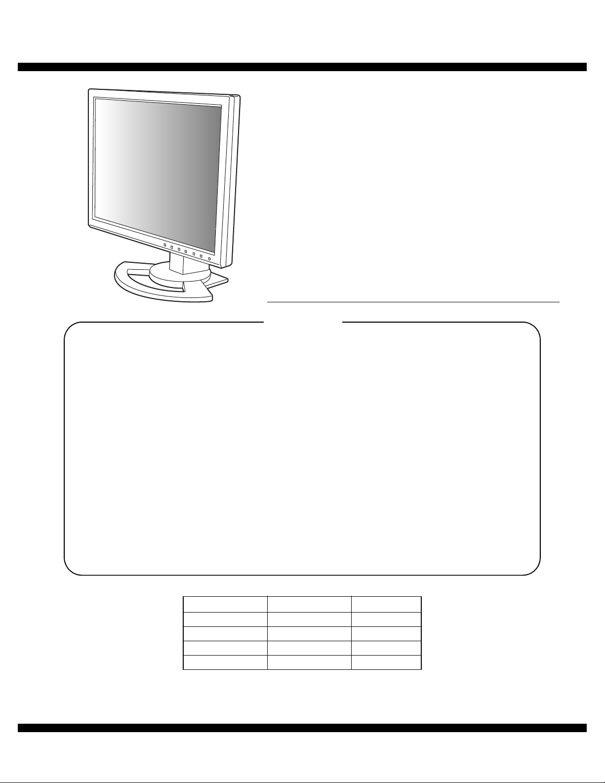
q
SERVICE MANUAL
CODE : 00ZLLT1620ESE
LCD MONITOR
LL-T1520-E
LL-T1520-P
LL-T1620-E
MODEL
CONTENTS
CHAPTER 1. OUTLINE OF THE PRODUCT, NOMENCLATURE AND FUNCTION . . . 1 – 1
CHAPTER 2. CONNECTION, ADJUSTMENT, OPERATION, AND FUNCTIONS . . . . . 2 – 1
CHAPTER 3. DISASSEMBLY AND ASSEMBLY. . . . . . . . . . . . . . . . . . . . . . . . . . . . . . . 3 – 1
CHAPTER 4. TROUBLE SHOOTING . . . . . . . . . . . . . . . . . . . . . . . . . . . . . . . . . . . . . . . 4 – 1
CHAPTER 5. BLOCK DIAGRAM. . . . . . . . . . . . . . . . . . . . . . . . . . . . . . . . . . . . . . . . . . . 5 – 1
CHAPTER 6. CIRCUIT DIAGRAM. . . . . . . . . . . . . . . . . . . . . . . . . . . . . . . . . . . . . . . . . . 6 – 1
CHAPTER 7. PARTS LAYOUT . . . . . . . . . . . . . . . . . . . . . . . . . . . . . . . . . . . . . . . . . . . . 7 – 1
LL-T1620-P
Product Name Model Name Color
LL-T1520-E LL-T1520-H Gray
LL-T1520-P LL-T1520-B Black
LL-T1620-E LL-T1620-H Gray
LL-T1620-P LL-T1620-B Black
Parts marked with "!" are important for maintaining the safety of the set. Be sure to replace these parts with specified
ones for maintaining the safety and performance of the set.
This document has been published to be used
SHARP CORPORATION
for after sales servic e only.
The contents are subject to change without notice.
Page 2
PC-UM10M
CHAPTER 1. OUTLINE OF THE PRODUCT, NOMENCLATURE AND FUNCTION
1. SPECIFICATIONS
LL-T1520 LL-T1620
LCD panel Diagonal 38cm Diagonal 40cm
Advanced Super-V and Anti-GlareLow Reflection TFT LCD module
Resolution (max.) XGA, 1,024 x 768 pixel SXGA, 1,280 x 1,024 pixel
Displayable colors (max.) Approx. 16.77 million color (8 bit)
Brightness (max.) 250 cd/m
Dot pitch 0.297(H) x 0.297 (V)mm 0.248(H) x 0.248 (V)mm
Contrast ratio 400 : 1
Angle of visibility Left-right 170°; Up-down 170°
Screen display size Horizontal 304.1 x Vertical 228.1 mm Horizontal 317.4 x Vertical 253.9 mm
Video signal Analog:Analog RGB (0.7 Vp-p) [75Ω]
Digital: DVI standard 1.0 compatible
Sync signal H/V separate Sync (TTL level: +/-), Sync on Green, Composite Sync (TTL level:+/-)
Expansion compensation Digital screening
(Enlargement VGA/SVGA etc. to full screen size. )
Plug & Play VESA DDC1/DDC2B compatible
Power management VESA DPMS, DVI DMPM
Speaker output 1W + 1W
Input signal terminal Mini D-sub 15 pin (3 row), DVI-I 29 pin
Audio input terminal Mini stereo jack
Headphone terminal Mini stereo jack
Screen tilt Upward approx.0° -30°; downward approx.0° - 5°
Screen swivel Approx.90° from left through right
Power supply AC100 - 240V, 50/60Hz
Temperature of
operating environment
Power consumption Maximum 36W (Standby state: 3W) Maximum 42W (Standby state: 3W)
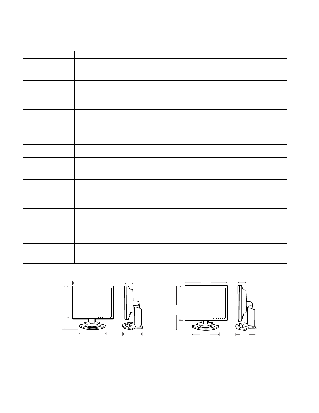
Dimensions 337(W) x 185(D) x 355(H) mm 352(W) x 185(D) x 370(H) mm
Weight Approx. 4.9kg
5 - 35°C
(approx. 3.3kg excluding stand)
2
300 cd/m
Digital screening
(Enlargement VGA/SVGA/XGA etc. to full screen size. )
Approx. 5.3kg
(approx. 3.7kg excluding stand)
2
■
■ DIMENSIONS (Units: mm)
■ ■
337
270
61
LL-T1520
355
238
185
Cable
Analog signal cable: Approx. 2.0m
Audio cable: Approx. 2.0m
Digital signal cable, NL-C01E (purchased separately): Approx. 2.0m
Analog signal cable, NL-C02E (purchased separately): Approx. 2.0m
LL-T1520-H/B LL-T1620-H/B OUTLINE OF THE PRODUCT, NOMENCLATURE AND FUNCTION
1 – 1
370
298
352
LL-T1620
238
64
185
Page 3
PC-UM10M
Relevant signal timings
Display mode
VESA
US text
Power
Macintosh
series
Sun Ultra
series
640 x 480
800 x 600
1024 x 768
1152 x 864
1280 x 960
1280 x 1024
720 x 400
640 x 480
832 x 624
1024 x 768
1152 x 870
1280 x 1024
1024 x 768
1152 x 900
1280 x 1024
Hsync
31.5kHz
37.9kHz
37.5kHz
35.1kHz
37.9kHz
48.1kHz
46.9kHz
48.4kHz
56.5kHz
60.0kHz
67.5kHz
60.0kHz
64.0kHz
80.0kHz
31.5kHz
35.0kHz
49.7kHz
60.2kHz
68.7kHz
64.0kHz
80.0kHz
48.3kHz
53.6kHz
56.6kHz
61.8kHz
71.7kHz
Vsync
60Hz 25.175MHz
72Hz 31.5MHz
75Hz 31.5MHz
56Hz 36.0MHz
60Hz 40.0MHz
72Hz 50.0MHz
75Hz 49.5MHz
60Hz 65.0MHz
70Hz 75.0MHz
75Hz 78.75MHz
75Hz 108.0MHz
60Hz 108.0MHz
60Hz 108.0MHz
75Hz 135.0MHz
70Hz 28.3MHz
66.7Hz 30.2MHz
74.6Hz 57.3MHz
75Hz 80.0MHz
75Hz 100.0MHz
60Hz 108.0MHz
75Hz 135.0MHz
60Hz 64.13MHz
66Hz 70.4MHz
70Hz 74.25MHz
66Hz 94.88MHz
67.2Hz 117.01MHz
Dot frequency LL-T1520 LL-T1620
ANALOG DIGITAL ANALOG DIGITAL
||||
||||
||||
|-|-
||||
||||
||||
||||
||||
||||
--||
--||
--||
--|-
||||
|-|-
|-|-
|-|-
--|-
--|-
--|-
--|-
--|-
--|-
--|-
--|-
• Recommended resolution for LL-T1520 is 1024 x 768.
• Recommended resolution for LL-T1620 is 1280 x 1024.
• All are compliant only with non-interlaced.
• The monitor can be connected to the following computers that have a
DVI standard output terminal (DVI-D24 pin or DVI-I29 pin) for digital
connection. (Note that the display may not appear correctly, depending on the connected computer.)
-- LL-T1520: Computers capable of XGA output
-- LL-T1620: Computers capable of SXGA output
• Frequencies for Power Macintosh and the Sun Ultra series are reference values. To connect, another adapter (commercially available)
may be required.
• If the monitor is receiving timing signals that are not compatible, [OUT
OF TIMING] will appear. Follow your computer's instruction manual
to set the timing so that it is compatible with the monitor.
• If the monitor is not receiving any signal (synch signal), [NO SIGNAL]
will appear.
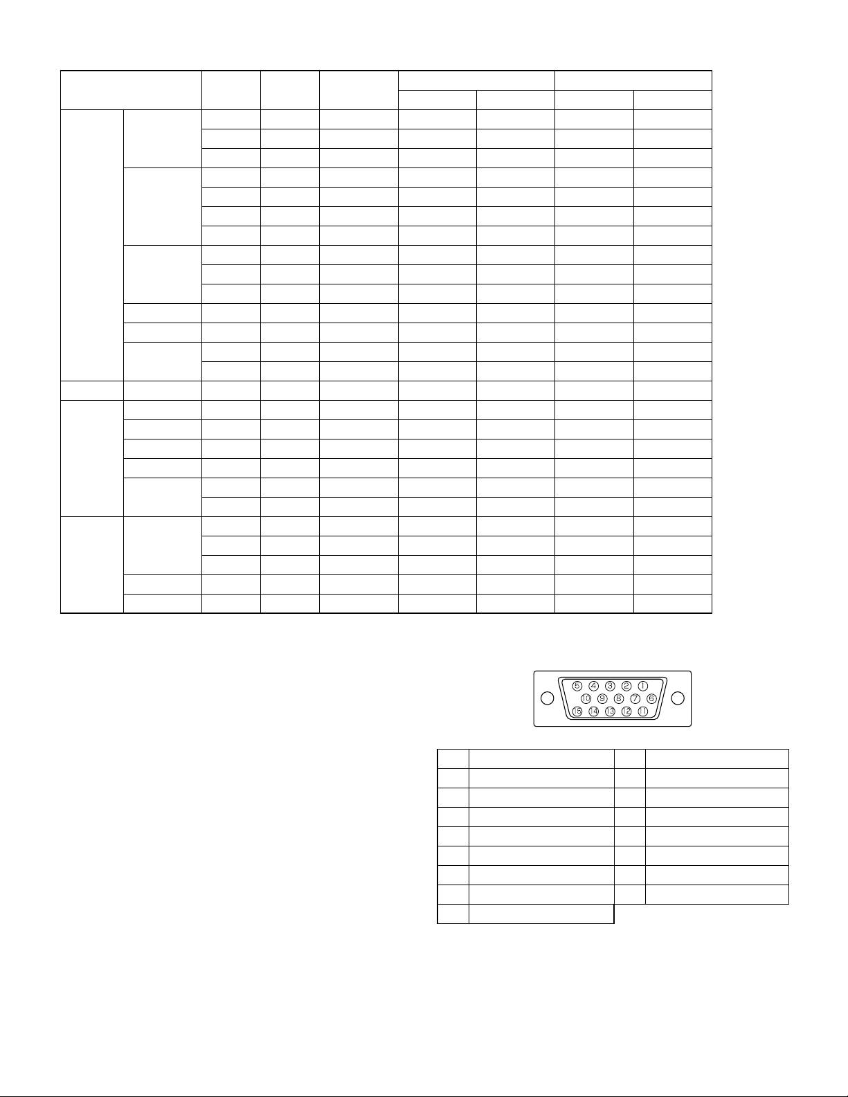
The analog RGB input connector pin
(Mini D-sub connector with 15 pins)
No. Function
1 Red video signal input
2 Green video signal input
3 Blue video signal input
4GND
5GND
6 For red video signal GND
7 For green video signal GND
8 For blue video signal GND
No.
9
10
11
12
13
14
15
Function
DDC/+5V
GND
N.C.
DDC data
For Hsync signal input
For Vsync signal input
DDC clock
LL-T1520-H/B LL-T1620-H/B OUTLINE OF THE PRODUCT, NOMENCLATURE AND FUNCTION
1 – 2
Page 4
PC-UM10M
The DVI-I input connector pin
(DVI-I connector with 29 pins)
C1 C2
C3 C4 C5
No. Function No. Function
1
TMDS data 2-
2
TMDS data 2+
3
TMDS data 2/4 shield
4
N.C.
5
N.C.
6
DDC clock
7
DDC data
8
Analogue vertically
synchronised signal
9
TMDS data 1-
10
TMDS data 1+
11
TMDS data 1/3 shield
12
N.C.
13
N.C.
14
+5V
15
GND
16
Hot plug detection
17
TMDS data 0-
18
TMDS data 0+
19
TMDS data 0/5 shield
20
N.C.
21
N.C.
22
TMDS clock shield
23
TMDS clock +
24
TMDS clock -
C1
Analogue red image signal
C2
Analogue green image signal
C3
Analogue blue image signal
C4
Analogue horizontally synchronised signal
C5
Analogue GND
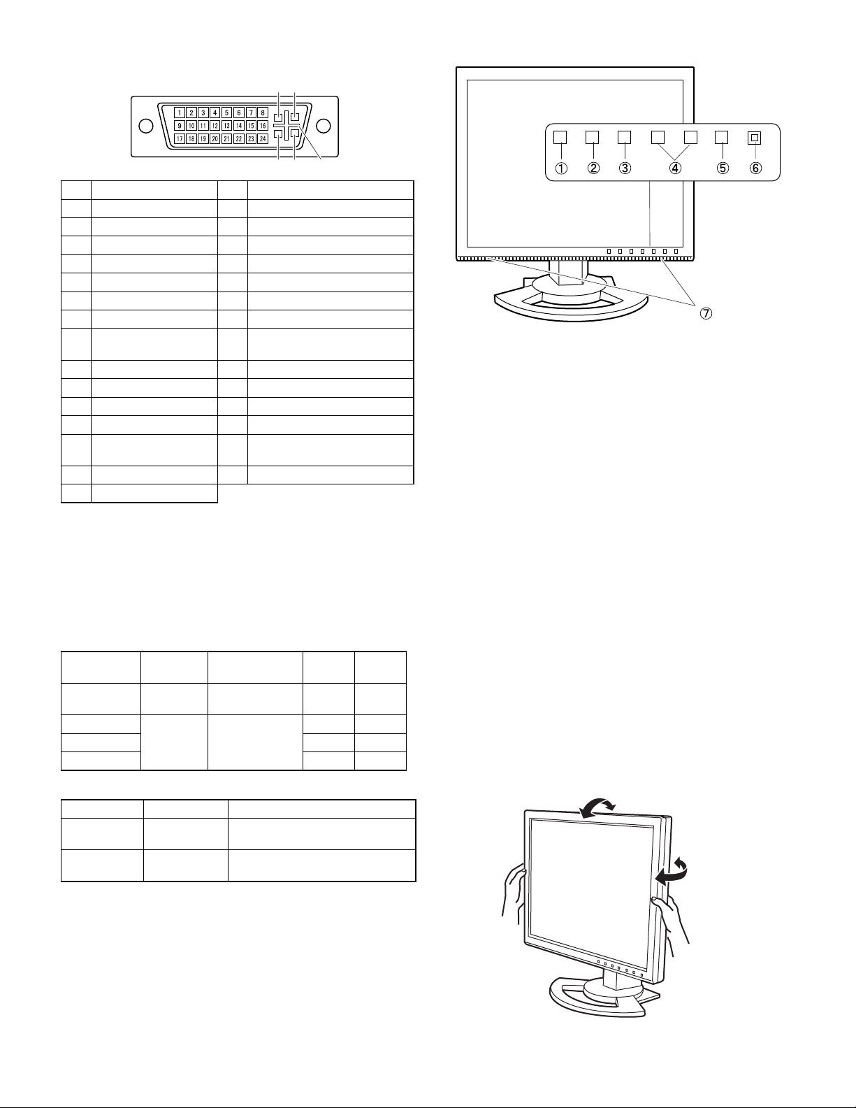
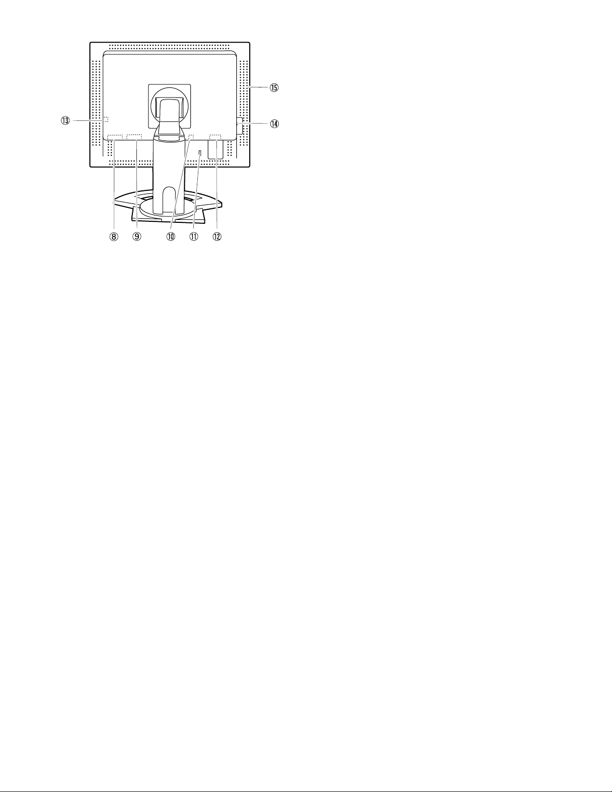
PRODUCT DESCRIPTION
1. INPUT button: To switch between the signal’s input terminals.
(Analogue RGB input terminal i DVI-I input termi-
nal)
2. MENU button: This button is used to pop-up, select and close the
OSD (On Screen Display) M enu.
3. SELECT button: This button is used to select menu options when
the OSD Menu i s displayed.
4. e d buttons: When the OSD Me nu is displayed:
These buttons are used to increa se or decre ase
the value of a selected option.
Power management
The monitor is based on the VESA DPMS*1 and the DVI DMPM*2 standards.
To activate the monitor's Power Management function, both the video
card and the computer must conform to the VESA DPMS standard and
the DVI DMPM standard.
*1 DPMS: Display Power Managem ent Signalling
DPMS mode Screen
ON
STANDBY
SUSPEND Yes No
OFF No No
*2 DMPM: Digital Monitor Power Management
DPMS mode Screen Power consumption
ON Display on LL-T1520: 36W
OFF Display off LL-T1520: 3W
Display on
Display off
Power
consumption
LL-T1520: 36W
LL-T1620: 42W
LL-T1520: 3W
LL-T1620: 3W
LL-T1620: 42W
H-sync V-sync
Yes Yes
No Yes
LL-T1620: 3W
DDC (Plug & Play)
When the OSD Menu is not displayed:
These buttons are used to adjust backlight bright-
ness and speaker volume.
5. Power button
6. Power LED: This LED is lit green when in use and orange when
in power-saving mode.
7. Speakers Audio entering via the monitor and the external
device connected to the monitor can be heard.
Adjusting the tilt and the swivel of monitor
Lightly holding both sides of the monitor, adjust it to a suitable viewing
angle.
Note: When adjusting the screen tilt and swivel, pressure from hands
on the LCD panel could cause damage.
approx.30˚
approx.5˚
approx.45˚
approx.45˚
This monitor supports the VESA DDC (Display Data Channel) standard.
DDC is a signal standard for carrying out Plug & Play functions on the
monitor or PC. It transfers information such as degree of resolution
between the monitor and PC. You can use this function if your PC is
DDC compliant and if it is set so that it can detect the Plug & Play monitor.
There are many varieties of DDC due to the differences between systems. This monitor works with DDC1 and DDC2B.
LL-T1520-H/B LL-T1620-H/B OUTLINE OF THE PRODUCT, NOMENCLATURE AND FUNCTION
1 – 3
Page 5
PC-UM10M
.
8. DVI-I input terminal: T h e com pu ter’ s d igita l RGB out pu t ter mi nal or a nal ogue RGB
output terminal can be connected here.
• The monitor can be connected to the following computers
that have a DVI standard output terminal (DVI-D24 pin or
DVI-I29 pin) for digital connection. (Note that the display may
not appear correctly, depending on the connected computer.)
-- LL-T1520: Computers capable of XGA output
-- LL-T1620: Computers capable of SXGA output
• Separately sold cables are necessary for connection.
To connect to a digital RGB output terminal:
-- Digital signal cabl e (model name: NL-C01E)
To connect to an analog RGB output terminal:
-- Analog signal cable (model name: NL-C02E)
9. Analog RGB input
terminal:
The analog signal cable is connected here.The analog signal
cable included should be used.
10. Audio input terminal: A computer's audio output terminal can be connected here .
The audio cable included should be used.
11. Security lock anchor: By connecting a security lock (commercially available) to the
security lock anchor, the monitor is fixed so that it cannot be
transported.
The security slot works in conjunction with Kensin gton Micro
Saver Security Systems.
12. Power terminal:
13. Headphone terminal: Headphones (commercially avai lable) can be connected here.
14. Main power switch
15. Ventilation openings:
Note: Never block the ventilation open ings as this may l ead to
overheating inside the monitor and result in malfunction.
LL-T1520-H/B LL-T1620-H/B OUTLINE OF THE PRODUCT, NOMENCLATURE AND FUNCTION
1 – 4
Page 6

PC-UM10M
CHAPTER 2. CONNECTION, ADJUSTMENT, OPERATION, AND FUNCTIONS
1. CONNECTING THE MONITOR AND TURNING THE MONITOR ON AND OFF
Caution: • When connecting, ensure that both the monitor and com-
puter are switched off.
• Be careful not to overly bend the cable or add extension
cords as this could lead to malfunction.
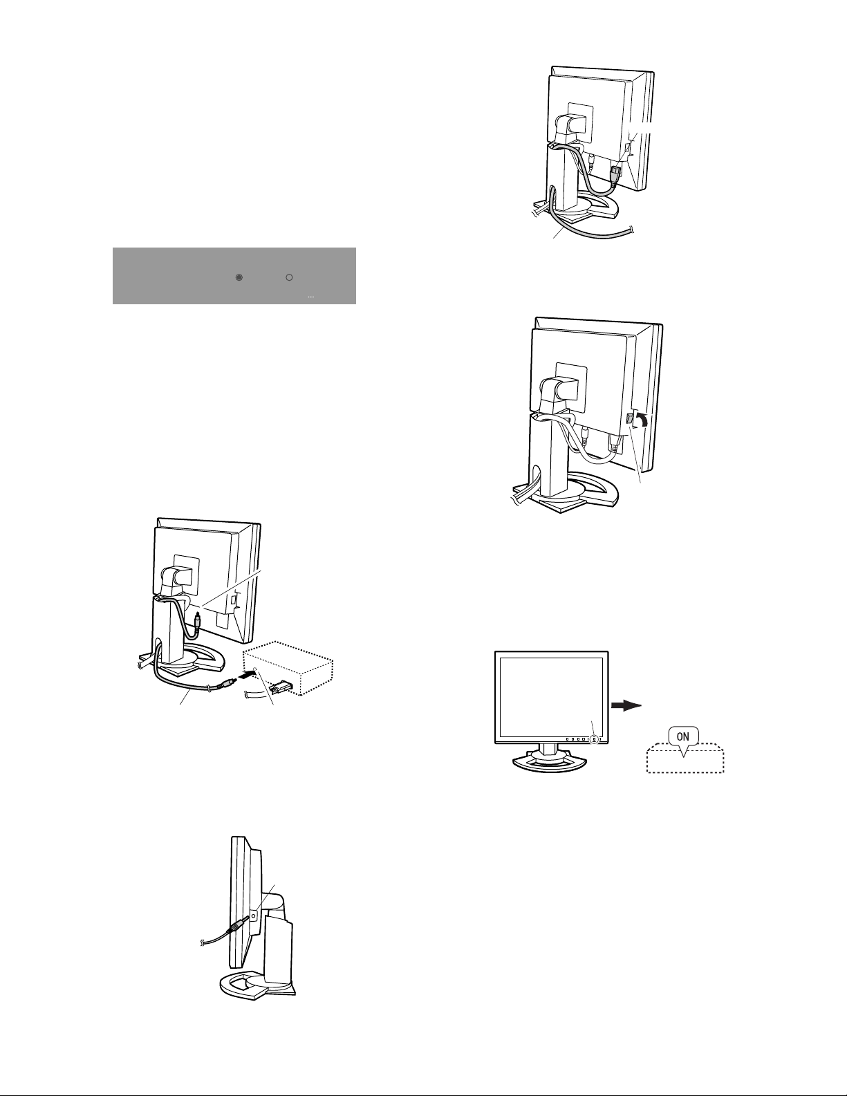
Cable storage
If necessary, excess cable can be housed in the stand.
1. Remove the cover.
Gently pull the top of the cover towards yourself.
CONNECTING THE MONITOR TO A COMPUTER
Connecting using accessory analog signal cable
Connect the accessory analog signal cable to the analog RGB input terminal of the display, and the analog RGB output terminal of the computer.
Analog RGB input
terminal
2. Run cable along the back of the stand.
3. Refit the cover.
Be careful not to pinch the cable.
Analog signal cable
• Paying attention to connector direction, firmly insert the signal
cable to terminal, and then tighten the screws at both sides.
If connecting to a D-sub 15 pin 2 row Apple P ower Macintosh, attach a
Macintosh conversion adapter (commercially available) to the analog
signal cable.
Macintosh conversion adapter
Analog RGB output terminal
Connecting using a separately sold display cable
The separately sold display cable enables connection between the DVII input terminal on the display and the digital or analog RGB output terminal of the computer.
When connecting to a digital RGB output terminal:
• Use a digital signal cable (model name: NL-C01E)
• The monitor can be connected to the following computers that have a
DVI standard output terminal (DVI-D24 pin or DVI-I29 pin) for digital
connection. (Note that the display may not appear correctly, depending on the connected computer.)
-- LL-T1520: Computers capable of XGA output
-- LL-T1620: Computers capable of SXGA output
When connecting to an analog RGB output terminal:
• Use an analog signal cable (model name: NL-C02E).
• If the cover is hard to refit, do not force it.
Check whether cables are trapped.
LL-T1520-H/B LL-T1620-H/B CONNECTION, ADJUSTMENT, OPERATION, AND FUNCTIONS
2 – 1
DVI-I input terminal
Display cable
(to be purchased separately)
RGB output terminal
Page 7
PC-UM10M
• Paying attention to connector direction, firmly insert the signal
cable to terminal, and then tighten the screws at both sides.
Set the monitor as follows when establishing a digital connection with a
Power Mac using an ADC-DVI adapter made by Belkin. (Operation has
been checked with the Power Mac G4 M7627J/A)
• Perform settings with the Power Mac power supply off.
• The setup screen automatically disappears approximately 30 seconds after the last command.
1. After connecting the power cord, turn on the monitor’s main power.
2. Press the e button and d button simultaneously, and while doing
this press the POWER button (i.e. turn the power on).
MAC DIGITAL
INPUT-2
OFF
ON
OK [ MENU ]
3. Set to “ON” with the e d buttons.
• Do not set to [ON] if you are not using a Belkin ADC-DVI adapter, as
this may result in incorrect display.
4. Press the MENU button.
This completes setting.
CONNECT THE ACCESSORY AUDIO CABLE
When the accessory audio cable is connected to the audio output terminal of the computer, the sound of the connected computer is output
from the display speakers. You can also use the headphone jack of the
display.
CONNECTING THE MONITOR TO A POWER SOURCE
Power terminal
AC outlet
Power cord
TURNING THE POWER ON
1. Turn on the main power of the monitor.
Main power switch
Audio input
terminal
Audio cable
Audio output terminal
• If you plan to use a commercially available cable, obtain one with no
resistance.
CONNECTION OF HEADPHONES
(COMMERCIALLY AVAILABLE)
Headphones (commercially available) can be connected.
Headphone
terminal
Headphones
• When switching the main power switch on and off, always wait
for an interval of at least 5 seconds. Rapid switching may result
in malfunction.
2. Press the monitor’s POWER button.
The power LED will light up orange.
3. Turn on the computer.
Turn on the computer
Press power button
power supply.
When a signal is input from the computer, the power LED lights up
green, and the screen is displayed (After power is turned on, it may
take a little time until the screen is displayed.)
• If the input terminal to which the computer is connected has not
been selected, the screen will not be displayed. If necessary,
perform input terminal switching.
Notes: (when using an analog signal)
• If using the monito r for the first time or after having changed the system settings during use, perform an automatic screen adjustment.
Note: When the headphones are co nnected, no sound can be heard
from the monitor speakers.
LL-T1520-H/B LL-T1620-H/B CONNECTION, ADJUSTMENT, OPERATION, AND FUNCTIONS
• When connecting to a notebook, if the notebook computer’s screen is
set so that it is displaying at the same time, the MS-DOS screen may
not be able to display properly. In this case, change the settings so
that only the monitor is displaying.
2 – 2
Page 8
PC-UM10M
CHANGING BETWEEN INPUT TERMINALS
Use the INPUT button to switch between signal input terminals.
Analog RGB input terminal
INPUT-1
<ANALOG>
DVI-I input terminal
(digital)
INPUT-2
<DIGITAL>
INPUT
DVI-I input terminal
(analog)
INPUT-2
<ANALOG>
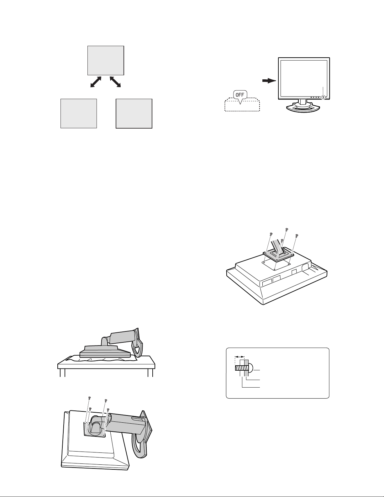
TURNING THE POWER OFF
1. Turn the computer off.
2. Press the monitor’s POWER button.
The Power LED will disappear.
Turn on the
computer off
If the monitor will not be used for a long time, turn off the main power
switch of the monitor, and remove the power plug from the outlet.
2. INSTRUCTIONS FOR ATTACHING A VESA COMPLIANT ARM
An arm or stand based on the VESA standard (comme rcially available)
can be attached to the monitor.
Procurement of the arm or stand is at the customer’s discretion.
Arms or stands able to be used
Attachments must satisfy the following.
• Compatible with the VESA standard
• Ha ve a gap of 75 mm x 75 mm between the screw holes on the section to be attached
• Not be likely to fall off or break off after being attached to the monitor.
Notes: • The stand is specially made for use with this monitor. Once
having removed the stand, never attempt to attach it to
another device.
• Once having removed the screws, store them together with
the stand and if the stand is ever re-attached be sure to use
the original screws. Using different screws could lead to a
malfunction.
6. Attach the arm to the monitor with the four screws.
Press power button
How to attach the arm or stand
• Be careful not to overly bend the cable or add extension cords as this
could lead to malfunction.
• While following these instructions, please also refer to the installation
instructions in the operation manual included with the arm or stand.
1. Turn off the monitor’s power and unplug AC plug from AC outlet.
2. Remove the cable.
3. Spread out a soft cloth on a suitable horizontal surface.
4. Being careful not to damage the monitor, gently lay the monitor on it
display-side down.
5 Remove the four screws and then remove the stand from the moni-
tor.
Note: The screws used to attach the arm should be M4 screws with a
length of 6 mm ~ 8 mm protruding from the surface to be
attached. Using different screws could lead to malfunction or may
lead to the monitor falling off, internal damaged, personal injury.
6 ~ 8 mm
Screw used to attach arm
Arm
Part of monitor to which
arm is attached
LL-T1520-H/B LL-T1620-H/B CONNECTION, ADJUSTMENT, OPERATION, AND FUNCTIONS
2 – 3
Page 9

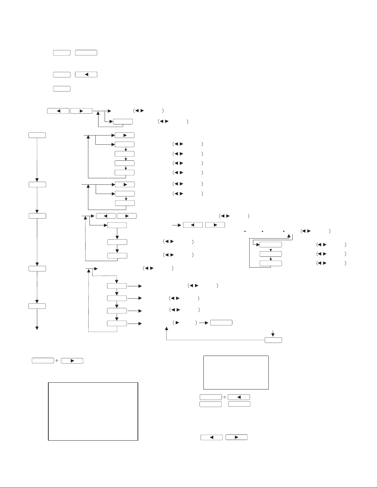
3. ADJUSTMENT
3-1. ADJUSTMENT METHOD
1) Resetting all adjustment values
+
MENU
Press the above two buttons at same time, and while turn the power on.
2) ADJUSTMENT menu reset
MENU
3) Adjustment lock function
MENU
While pressing the MENU button, turn the power on.
4) Adjusting the Backlight or Volume
5) Screen adjustment
MENU
ADJUSTMENT AUTO
(for ANALOG)
GAIN
MENU
CONTROL
(For ANALOG)
COLOR
MENU
CONTROL
MENU
MODE SELECT
SELECT
+
Power ON
Power ON
Press the two buttons at same time.
OSD H-POSITION
BRIGHT
SELECT
SELECT
SELECT
SELECT
SELECT
SELECT
SELECT
SELECT
SELECT
SELECT
buttons
VOLUME
CLOCK
PHASE
H-POS
V-POS
AUTO
BLACK LEVEL
buttons
buttons
buttons
buttons
buttons
buttons
buttons
CONTRAST
COLOR MODE (sRGB, STD, VIVID)
buttons
WHITE BALANCE WHITE BALANCE
COOL STD
HUE
SATURATION
buttons
buttons
buttons
WARM USER
SELECT
SELECT
SELECT
R-CONTRAST
G-CONTRAST
B-CONTRAST
PC-UM10M
buttons
buttons
buttons
buttons
SELECT
SELECT
MENU
SELECT
SELECT
END
6) Version display (for service)
Power ON
MENU
Display the software version.
With the version displayed, no button operations are valid.
< VERSION & CHECK SUM >
VERSION : 1.04 (20020411)
CHECK SUM : OK A02D
HS
OSD V-POSITION
SCALING
400 LINES
LANGUAGE
buttons
buttons
buttons
button
SELECT
(English, German, French, Dutch,
Spanish, Italian, Swedish, Japanese)
7) Test 1 (for service)
DIAG TOOL MENU
AGING TEST 1
AGING TEST 1
SET••• [MENU]
SELECT
Power ON
SELECT
Blue
H
H
White H Black
MENU
3
Green H Red H Dark blue H Dark green H Dark red
8) Test 2 (for service)
H
Green
H
Red
Flicker pattern
Blue
H
Checker pattern
When the test is terminate, Power off
H
MENU
White
H
H
Black
H
Gray scale
LL-T1520-H/B LL-T1620-H/B CONNECTION, ADJUSTMENT, OPERATION, AND FUNCTIONS
2 – 4
Page 10
3. ADJUSTMENT
3-1. ADJUSTMENT METHOD
1) Resetting all adjustment values
+
MENU
Press the above two buttons at same time, and while turn the power on.
2) ADJUSTMENT menu reset
MENU
3) Adjustment lock function
MENU
While pressing the MENU button, turn the power on.
4) Adjusting the Backlight or Volume
5) Screen adjustment
MENU
ADJUSTMENT AUTO
(for ANALOG)
GAIN
MENU
CONTROL
(For ANALOG)
COLOR
MENU
CONTROL
MENU
MODE SELECT
SELECT
+
Power ON
Power ON
Press the two buttons at same time.
OSD H-POSITION
BRIGHT
SELECT
SELECT
SELECT
SELECT
SELECT
SELECT
SELECT
SELECT
SELECT
SELECT
buttons
VOLUME
CLOCK
PHASE
H-POS
V-POS
AUTO
BLACK LEVEL
buttons
buttons
buttons
buttons
buttons
buttons
buttons
CONTRAST
COLOR MODE (sRGB, STD, VIVID)
buttons
WHITE BALANCE WHITE BALANCE
COOL STD
HUE
SATURATION
buttons
buttons
buttons
WARM USER
SELECT
SELECT
SELECT
R-CONTRAST
G-CONTRAST
B-CONTRAST
PC-UM10M
buttons
buttons
buttons
buttons
SELECT
SELECT
MENU
SELECT
SELECT
END
6) Version display (for service)
Power ON
MENU
Display the software version.
With the version displayed, no button operations are valid.
< VERSION & CHECK SUM >
VERSION : 1.04 (20020411)
CHECK SUM : OK A02D
HS
OSD V-POSITION
SCALING
400 LINES
LANGUAGE
buttons
buttons
buttons
button
SELECT
(English, German, French, Dutch,
Spanish, Italian, Swedish, Japanese)
7) Test 1 (for service)
DIAG TOOL MENU
AGING TEST 1
AGING TEST 1
SET••• [MENU]
SELECT
Power ON
SELECT
Blue
H
H
White H Black
MENU
3
Green H Red H Dark blue H Dark green H Dark red
8) Test 2 (for service)
H
Green
H
Red
Flicker pattern
Blue
H
Checker pattern
When the test is terminate, Power off
H
MENU
White
H
H
Black
H
Gray scale
LL-T1520-H/B LL-T1620-H/B CONNECTION, ADJUSTMENT, OPERATION, AND FUNCTIONS
2 – 4
Page 11

PC-UM10M
CHAPTER 3. DISASSEMBLY AND ASSEMBLY
[Note for works]
For disassembly and assembly procedures of the pa rts which are not
described in this section, refer to the Parts Guide.
For assembly, reverse the disassembly procedures.
Use an earth band for disassembly and assembly works.
* DISASSEMBLY FLOW CHART
1. Separation of the display
section and the stand section
3. Separation of stand base
3
section from stand arm
section disassembly
44
2. Display cover disassembly 3-1. Stand arm section disas-
sembly
44
2-1. Power PWB, Sound PWB,
Main PWB disassembly
3-2. Hinge section disassembly
44
2-2. Separation of the LCD sec-
tion and the display mask
section
3-3. Stand base section disas-
sembly
4
2-3. Inverter PWB and LCD unit
disassembly
4
2-4. Key PWB disassembly
1. Separation of the display section and the stand section
1. Remove four screws 1 and separate the stand section 2 and
the display section 3.
3
2. Display cover disassembly
1. Remove seven screws 1, and remove the display cover 2.
2
1
1
1
1
1
2-1. Power PWB, Sound PWB, Main PWB disassembly
1. Remove the P/S SW cover 1 and the HH jack cover 2.
2. Remove eight screws 3, and remove the shield plate 4.
3. Remove the connector 5 and four screws 6, and remove the
power PWB 7.
4. Remove the connector 8 and two screws 9, and remove the
sound PWB F.
5. Remove the connector G (LL-T1520(7 positions) LL-T1620(six
positions)) and seven screws H.
6. Remove four hex screws I, and remove the main PWB K
from the connector angle J.
11
15
11
LL-T1620H/B
LL-T1520H/B
12
1
1
2
LL-T1520-H/B LL-T1620-H/B DISASSEMBLY AND ASSEMBLY
3 – 1
3
2
3
[Note for assembly]
When assembling the P/S SW cover 1 and the HH jack cover 2, be
sure to engage the pawls securely.
When connecting connector A to the main PWB, place the connector
A with the character surface upward.
4
3
3
11
A
11
15
11
12
12
1
12
13
11
10
8
A
9
14
5
7
6
6
Page 12

PC-UM10M
2-2. Separation of the LCD section and the display mask
section
1. Remove three screws 1, and separate the LCD section 2
from the display mask section 3.
3
2
1
1
1
2-3-1. Inverter PWB and LCD unit disassembly
(LL-T1520H/B)
1. Remove three screws 1 and two screws 2, and remove the
LCD base angle 3.
2. Remove two connector disconnection prevention sheets 4,
and remove the connector 5 at 5 positions.
3. Remove four screws 6, and remove the inverter PWB 7.
4. Remove two screws 8, and remove the LCD angle 9.
5. Remove the connector F at two positions from the LCD unit G.
2-3-2. Inverter PWB and LCD unit disassembly
(LL-T1620H/B)
1. Remove three screws 1 and two screws 2, and remove t he
LCD base angle 3.
2. Remove two connector disconnection prevention sheets 4,
and remove the connector 5 at 5 positions.
3. Remove four screws 6, and remove the inverter PWB 7.
4. Remove two screws 8, and remove the LCD angle 9.
5. Remove the connector F from the LCD unit G
8
5
7
6
4
5
8
11
9
6
4
5
10
1
2
3
2-4. Key PWB disassembly
1. Remove four screws 1, and remove the Speaker unit 2.
2. Remove nine screws 3, and remove the Key SW angle 4.
3. Remove the connector 6 from the key PWB 5.
5
6
11
2
5
7
4
2
3
6
5
8
9
3
1
10
5
4
3
6
1
8
1
2
LL-T1520-H/B LL-T1620-H/B DISASSEMBLY AND ASSEMBLY
3 – 2
Page 13

PC-UM10M
3. Separation of stand base section from stand arm sectio n
disassembly
1. Remove four screws 1, and separate the stand base section
2 from the stand arm section 3.
3
2
3-2. Hinge section disassembly
1. Remove screw 1, and remove the Hinge cover C 2.
2. Remove screw 3, and remove the Hinge cover B 4.
3. Remove the screw 5, and remove the Hinge cover A 6 from
the hinge unit 7.
6
4
5
7
3
1
2
1
1
3-1. Stand arm section disassembly
1. Remove the cable cover 1.
2. Remove four screws 2, and remove the base arm cover B 3.
3. Remove the base arm cover F 4.
4. Remove three screws 5 and three washers 6, and remove the
base arm install angle 7.
5. Remove two screws 8 and two washers 9, and remove the
hinge section F.
10
8
9
9
8
3-3. Stand base section disassembly
1. Remove five rubber seat 1.
2. Remove seven screws 2, and remove the stand base plate A
3.
3. Remove the stand base plate B 4 from the stand cover 5.
5
4
4
3
3
5
2
1
6
2
7
5
6
5
LL-T1520-H/B LL-T1620-H/B DISASSEMBLY AND ASSEMBLY
3 – 3
1
1
2
1
2
1
2
2
Page 14

PC-UM10M
CHAPTER 4. TROUBLE SHOOTING
First of all, check to confirm that all the accessory cables below are
properly connected.
Also check to confirm that the PC's video mode is set to match the signal timing supported by this machine.
The display does not work (with analog signal input, RGB cable)
When the power button is pressed, does the
LED turn green ?
(Yes)
Does B/L light up ?
(Yes)
Is the display normal in each video mode ?
(Yes)
No abnormality
1
Is the AC cable connected to the power unit ?
(Yes)
Is the power unit switch ON ?
(Yes)
Is the input signal port connected to the analog
signal cable ?
(Yes)
Is DC+12V supplied to CN16-1P ?
(Yes)
Is IP2 at DC+5V ? (LL-T1520H/B only)
(Yes)
Is IP3 at DC+5V ? (LL-T1620H/B only)
(Yes)
Is FB30 at DC+3.3V ?
(Yes)
Are FB20 and FB29 at DC+2.5V ?
(Yes)
Is X1 oscillating ?
(Yes)
Is RESET signal delivered from IC23 ?
(Yes)
Is the level of IC13-85P changed by turning
ON/OFF the power button ?
(Yes)
Are signals of R19 and R71 normal ?
(Yes)
Are the addresses and data signal of IC13 and
IC17 correct ?
(Yes)
Is the signal at IC13 39 40pin normal ?
(Yes)
Are signals of R112 and R113 normal ?
(Yes)
Check the SW PWB , the SW cable, and their
connection.
* Accessory cables
• Exclusive-use AC cable
• Exclusive-use analog signal cable (RGB cable)
• Exclusive-use digital signal cable (DVI-D cable)
Perform 1
(No)
Perform 2
(No)
Perform 3
(No)
(No)
Check the AC cable connection.
(No)
Check the power unit switch.
Press the INPUT key to select the suitable
(No)
input signal port.
(No)
Check the power unit and the power cable.
Check IP2 and IC25 peripheral circuits.
(No)
(No)
Check IP3 and IC24 peripheral circuit.
Check IC30 peripheral circuits.
(No)
(No)
Check IC10 and IC20 peripheral circuits.
(No)
Check X1 and peripheral circuits.
(No)
Check IC23 and peripheral circuits.
Check XPON signal and CN7 peripheral
(No)
circuits.
Check the analog signal cable and CN2
(No)
peripheral circuits and IC5 peripheral circuits.
(No)
Check IC13 and IC17 peripheral circuits.
Check EDSDA signal, EDSCL signal, IC13
(No)
and IC21 peripheral circuits.
(No)
Check Q6 Q7, and peripheral circuits.
LL-T1520-H/B LL-T1620-H/B TROUBLE SHOOTING
4 – 1
Page 15

PC-UM10M
2
(Yes)
Is CN10-5P at H level (DC+3.3V) ?
(Yes)
Is CN10-6P at DC+1.0V or below when the
brightness is maximum ?
(Yes)
Is the inverter PWB normal ?
(Yes)
Check the lamp in the LCD module.
3
Check the power unit, the power cable, their
(No)Is FB23 at DC+12V ?
connection, the DC+12V power line, and IP1.
Check BLON signal and CN10 peripheral
(No)
circuits.
(No)
Check IC16 peripheral circuits.
Replace the inverter PWB unit.
(No)
(No)Are signals at IC13-17, 24, 40P normal ?
Check CN2, IC5, and IC13 peripheral circuits.
(Yes)
Check the analog signal cable, CN2
Are signals at R19 and R71 normal ?
(No)
peripheral, and IC peripheral circuits.
(Yes)
Is CN12-1P at DC+12V ? (LL-T1620H/B only) Check IP4 and IC25 peripheral circuits.
(No)
(Yes)
(No)Is CN9-39P at DC+5V ? (LL-T1520H/B only) Check IP2 and IC25 peripheral circuits.
(Yes)
Is the signal between IC13 and IC27 normal ?
(LL-T1620H/B only)
Check IC13 and IC27 peripheral circuits.
(No)
(Yes)
Is the signal between IC27 and CN12 normal ?
(LL-T1620H/B only)
Check IC27 and CN12K peripheral circuits.
(No)
(Yes)
(No)Is the signal between IC13 and CN9,C11 normal ?
(LL-T1520H/B only)
Check IC13, CN9, and 11 peripheral circuits.
(Yes)
(No)Are the cables of the LCD unit normal ? Check the cables and related parts.
(Yes)
Replace the LCD unit.
LL-T1520-H/B LL-T1620-H/B TROUBLE SHOOTING
4 – 2
Page 16

HSBC only
T1620 only
CCFT
CCFT
Back Light UnitBack Light Unit
T1520 only
HSBC Common
(16"S XGA)
(16"S XGA)
TFT LCD Unit
TFT LCD Unit
T1620
LCD-U
unit
Inverter
CCFT
CCFT
Back Light Unit
Back Light Unit
(15" XGA)
(15" XGA)
TFT LCD Unit
TFT LCD Unit
LCD-U
T1520/HSBC
LEDKey
KEY board
AC100~220V
unit
Power
supply
(NEW)
PC-UM10M
HEAD PHONE
SPEAKER OUT
3.3V
LVDS
LVDS
Display Data
2.5V
H/V
3.3V
(USER)
EEPROM
Engine
Graphic
RGB
Address
I2C
Sage
(S9330-100)
(T1620 S9330-135)
HVC
373
+5V
REG
REG
LCD 12V
3.3V
(Flash)
ROM8Mbit
+5V
+5V
REG
3.3V
REG
REG
2.5V
USB 5V
REG
REG
LCD 5V
+12V
USB 5V
AMP
AUDIO
CHAPTER 5. BLOCK DIAGRM
+5V
DDC)
(Analog
EEPROM
Selector
H/V
H/V
RGB
RGB
BUFF
RGB
H/V
DDC
LL-T1520-H/B LL-T1620-H/B BLOCK D I AGRM
DVI-I
DDC
5 – 1
DDC)
(Digital
EEPROM
Selector
DDC)
(Analog
EEPROM
USB
USB
IN
AUDIO
Main
Board
Page 17

PC-UM10M
A
1/6
D
4,5
RXD
SDA 3
TXD 4,5
SCL 3
C
B
12345678
A SEL 5
INPUT2 (DVI)
INPUT1 (RGB)
1
Q4
3 2
DTC114EUA
R72
4.7k
5V
TP224
L : IN2
H
L
A SEL
21
TP227
C68
2.2u
R31
R52
R38
R73
560
R91
10k
(3216)
180k 180k
R103
3.9k
NU
7.5k
R104
C59
0.1u
TP225
22
R105
C60
0.1u
C61
10u
A2.5V
Q3
C2412
1 3
2
TP226
2
TP228
1 3
Q5
R92
100k
C2412
3
33
R43
5V
1234567
IC7
2Y1
2Y0
3Y1
VCC
2-COM
1-COM
16151413121110
3-COM
1Y1
3Y0
1Y0AB
AGREEN- 5
ABLUE- 5
AVSYNC 5
AHSYNC 5
TP174
33
33
33
R81
R42
R80
R20
10K
R21
10K
8
INH
GND
GND
SN74LV4053A
C
9
3.3V
14
15
16
4A
XST
VCC
IC18
SELECT1A1B1Y2A2B2Y
1234567
C164
0.1u
111213
10
3A4Y4B
3B
74LVC157A
GND 3Y
8 9
NU
R69
NU
R17
5V
C3
TP176
33
33
R71
R19
TP160
R125
NU
R134
TP173
+
C21
0.1u
47u/16V
IC5
ABLUE+ 5
TP218
TP151
TP154
C15
22p
NU
100
100
R50
R30
R29
TP179
TP182
3.3V
C148
0
TP175
23
24
HIN2
HIN1
RIN1
HDET
123456789
C27
C16
1u (2125)
1u (2125)
0.1u
TP11
TP12
NU
R39
R33
19
20
21
22
VCC
ROUT
HOUT
GOUT
GIN1
GND
BIN1
GND
ARED+ 5
AGREEN+ 5
TP220
C26
22p
NU
R37
NU
17
18
CV_IN
CSOUT
RIN2
GND
R67
C33
1u (2125)
16
CTL
GIN2
TP155
C32
100
TP184
TP13
NU
R54
15
BOUT
GND
101112 13
ARED- 5
TP223
22p
NU
R51
14
VOUT
BA7657F
[CTL]
H : IN1
BIN2
VIN1 VIN2
LL-T1620H/B
5V
DDC5V
TP9
TP10
R57
10K
32
1
Q2
DTC114EUA
VPEN5
AVIN2
AHIN2
123
45
NCNCNC
GNDSDA
0.1u
C10
3
TP211
D4
RB715F
DDC5V
SCL
VCLK
VCC
BR24C21
IC6
678
1 2
TP4
R78
10k
R76
10k
TP6
TP5
1
23
1
23
DDC5V
D15
NU
D14
NU
IC11A
74LVC14
1
23
1
23
22
R106
1 2
TP213
200
R93
D18
NU
NU
D17
22
R109
IC11B
74LVC14
3 4
TP214
C63
39p
C62
39p
200
R94
R79
10k
R77
10k
GVSI
RGSL
INPUT1
CN2
TP215
TP216
TP217
TP219
TP221
TP222
C7 0.01u(B)
C9 0.01u(B)
C8 10uB(3216)
C6 10uB(3216)
C5 0.01u(B)
C4 10uB(3216)
TP177
INPUT2
ABIN2
NC
GHS
GND
GND
GNDNUGND
RGSA
DETECT
TP180
TP178
ARIN2
AGIN2
123456789101112131415
BIN
RIN
GIN
GND
CON 15P DISPIN
C29 0.01u(B)
C34 10uB(3216)
C36 10uB(3216)
TP183
TP185
C35 0.01u(B)
TP156
3.3V
IC11F
74LVC14
IC11C
74LVC14
C70
0.1u
R75
75
R56
75
R41
75
5 6
IC11E
13 12
R47
10K
XVPEN
LEDR1 5LEDR5
TP157
IC11D
74LVC14
74LVC14
9 8
11 10
VPEN5 5
C22 0.01u(B)
C28 10uB(3216)
TP181
CHAPTER 6. CIRCUIT DIAGRAM
ANALOG I/F
(1) MAIN PWB
D
C
LL-T1520-H/B LL-T1620-H/B CIRCUIT DIAGRAM
6 – 1
87654
B
A
Page 18

PC-UM10M
D
C
B
A
2/6
12345678
H
DIGITAL
100K
DIGITAL
DVI SEL
ANALOG
DIGITAL
LLH
VDD
R12
10k
21
123
0.1u
IC3
NCNCNC
VCC
R66
10k
R65
10k
SN74LV4053A
VCLK
678
TP193
45
GNDSDA
SCL
ANALOG EDID
BR24C21
TP195
NU
R168
3
R35
C44
TP188
R26
123
45
NCNCNC
0.1u
R45
R44
NU
R36
TP189
100
100
R27
GNDSDA
SCL
VCLK
VCC
IC9
10k
10k
NU
C18
678
TP190
TP191
16151413121110
0.1u
IC2
1234567
ZD1
NU
NU
ZD2
BR24C01
VCC
2Y1
R96
2-COM
2Y0
DIGITAL EDID
10k
1Y1
1-COM
3Y1
3-COM
C30
10k
R64
9
A
B
C
1Y0
3Y0
INH
GND
GND
8
RX2- 5
RX2+ 5
RX1- 5
TP152
TP153
RX0- 5
RX1+ 5
RX0+ 5
ARIN 1
AGIN 1
ABIN 1
RXC- 5
RXC+ 5
FB3 NU
FB2 NU
FB1 NU
R8
R9
R10
1
23
1
23
AVIN 1
AHIN 1
TP187
TP186
R14 22
TP230
IC4A
74LVC14
1 2
TP229
75
75
75
R6 200
D3
NU
NU
D2
5V
R46 22
TP232R15 200
IC4C
74LVC14
5 6
TP231
C1
39p
C2
39p
R16
10k
R7
NU
DVI SEL 5
1
Q1
3 2
DTC114EUA
R2
10K
TP234
TP233
R162
1234
INB
INA
R1
GNDOUT
4.7k
VCC
IC1
TC7SH32FU
5
TP8
TP7
123456789101112131415161718192021222324C1C2C3
A V
TX2-
TX4-
TX1-
TX3-
VDD
TX1+
TX0-
GND
GND
TX3+
TX0+
HPDETECT
GND
TX2+
TX4+
DCLK
CN1
(1) MAIN PWB
DDATA
DIGITAL I/F
D
10K
10K
R3
1k
R5
3
5V
D1
RB715F
C5
C4
A B
A R
A H
A G
TX5-
GND
GND
TXC-
TX5+
TXC+
A GND
TMDS
R4
TP235
1 2
3.3V
C31
0.1u
IC4E
74LVC14
11 10
IC4F
74LVC14
IC4B
74LVC14
IC4D
74LVC14
3 4
13 12
9 8
87654
C
LL-T1520-H/B LL-T1620-H/B CIRCUIT DIAGRAM
6 – 2
B
A
Page 19

PC-UM10M
3/6
12345678
BK2125LL560
FB16 BK2125LL560
R84
R83 NU
R82 NU
LCD & LVDS
D
GND
DCLK
GNDDEVSYNC
CN9
123456789
FL1
6
10
DBE7
DBE6
HSYNCNCGND
BE7
BE6
BE5
BE4
GND
BE3
BE2
BE1
BE0
GND
GE7
GE6
GE5
GE4
GND
GE3
GE2
GE1
10111213141516171819202122232425262728293031323334353637383940
1892345
1892345
FL3
FL2
7
6
7
10
ACA3216M300
ACA3216M300
DBE4
DBE5
DBE0
DBE2
DBE1
DBE3
GE0
1892345
FL4
6
7
DGE7
3.3V
6
10
ACA3216M300
DGE6
DGE5
DGE4
DGE3
DGE2
NU
FB31
C161
NU
+
TP236
NU
C160
NU
C136
NU
C135
NU
C134
NU
C146
NU
C158
NU
C159
10
CN10
GND
+12V
1234567
TP243
2Y0
2-COM
SCL
A
21
BL
+12V
GND
VON
VBR
NU
FB22
FBM2125HM330-T
TP244
TP245
TP246
FB17
FB21
ACB2012M-600
ACB2012M-600
C111
NU
TP148
TP149
TP150
TP1
123
4
RESET VALUE : L
AO1
AO2
AO3
AO4
SDA
SCL
GND
VCC
IC16
C150
82u/16V
5V
3Y1
1-COM
SDA
M62334FP
675
8
C113
0.1u
TP2
TP3
VOLUME4
AUSEL4
0
R18
NU
Q13
2 1
R13
NU
STBY4
8
INH
3Y0
GND
GND
3-COM
1Y1
1Y0AB
C162
SN74LV4053A
C
9
3
100
R95
BLON5
3
SDA 1
0.1u
C
GND
BO7
BO6
BO5
BO4
GND
BO3
BO2
BO1
BO0
GND
GND
RE7
RE6
RE5
RE4
GND
RE3
RE2
RE1
RE0
VLCD
VLCD
7
DGE1
1892345
DGE0
DRO0
DRO1
DRO2
DRO3
DRO4
DRO5
DRO6
DRO7
DGO0
DGO1
DGO2
DGO3
DGO4
DGO5
DGO6
DGO7
DBO0
DBO1
DBO2
DBO3
DBO4
GND
LCD40P
TP237
FB28
FBM2125HM330-T
LCD5V
1892345
1892345
FL5
FL6
6
7
6
10
ACA3216M300
DRE7
7
10
ACA3216M300
ACA3216M300
DRE1
DRE4
DRE2
DRE5
DRE6
DRE3
DRE0
CN12
VCC
VCC
VCC
GND
GND
GND
SELLVDS
BLON
123456789
12V
C129
NU
R137
NU
C130
R70
NU
3.3V
R107
NU
BR34 NU
BR33 NU
1 8
2 7
3 6
4 5
1 8
2 7
3 6
TB1-
TA1-
TC1-
TB1+
TA1+
IC27
NU
R10
51
R11
LVDS VCC
LVDS GND
52
R12
53
R13
54
VCC
55
GND
56
R14
57
R15
58
R16
59
R17
60
G10
61
G11
62
G12
63
G13
64
G14
65
G15
66
G16
67
G17
68
B10
69
B11
70
VCC
71
GND
72
B12
73
B13
74
B14
75
B15
B16
B17
R20
R21
R22
7677787980818283848586878889909192939495969798
DGND
RBIN3+
101112131415161718192021222324252627282930
TP238
NU
4 5
TC1+
TCLK1-
R23
R24
C88
0.1u
+
C87
33u/16V
FL7
10
RBIN3-
RBCLKIN+
RBCLKIN-
RBIN2+
RBIN2-
BR32 NU
1 8
2 7
3 6
4 5
TA2-
TD1-
TD1+
TCLK1+
LVDS GND
THC63LVD823
R25
R26
R27
VCC
GND
DBO7
RBIN1+
TA2+
G20
6
7
DBO6
DBO5
RBIN1-
RBIN0+
BR31 NU
1 8
TB2-
TB2+
G21
G22
CN11
123456789
1892345
ACA3216M300
DBO4
RBIN0-
RAIN3+
RAIN3-
RACLKIN+
2 7
3 6
4 5
TC2-
TC2+
TCLK2-
LVDS VCC
G23
G24
G25
G26
FL8
RACLKIN-
TCLK2+
G27
GO7
11121314151617181920212223242526272829303132333435
10
1892345
FL9
6
6
7
10
10
ACA3216M300
DGO7
DBO0
DBO1
DBO3
DBO2
DGO6
NU
RAIN2+
RAIN2-
RAIN1+
RAIN1-
RAIN0+
RAIN0-
LVDSGND
0
R139
BR30 NU
R140 0
1 8
2 7
3 6
4 5
26272829303132333435363738394041424344454647484950
TD2-
TD2+
PLL_GND
25
PLL_VCC
LVDS GND
24
PLL_GND
23
TEST5
22
TEST4
21
TEST3
20
XPDWN
19
6/8
18
OE
17
MODE0
16
MODE1
15
TEST2
14
TEST1
13
RS
12
R/F
11
CLKIN
10
DE
9
VSYNC
8
HSYNC
7
B27
6
B26
5
GND
4
VCC
3
B25
2
B24
1
B20
B21
B22
B23
99
100
B
GO6
GO5
GO4
GND
GO3
GO2
GO1
GO0
GND
RO7
RO6
RO5
RO4
GND
RO3
RO2
RO1
RO0
GND
GNDNCNCNCGND
LCD36P
36
1892345
1892345
FL11
6
7
10
ACA3216M300
DRO7
DRO6
DGO0
DGO1
BR29
NU
NU
Q11
3
NU
R135
1 2
NU
D19
NU
Q12
3
NU
R138
R/F : Input Clock Triggering Edge Select
( H - Rising, L - Falling )
RS : LVDS swing range select
( H - Normal, L - Reduced )
R136
4.7k
1892345
FL12
7
6
7
10
ACA3216M300
ACA3216M300
DRO2
DRO3
DRO1
DRO0
DRO5
DRO4
IP1
S2.3
FB23
4.7k
4.7k
SDA
45
GNDSDA
SCLWPVCC
678
FBM2125HM330-T
TP242
HN58X2416
5V
SCL 1
SCL
1234567
IC21
2Y1
VCC
16151413121110
3.3V
V12.5
5VSCL 3
5VSDA 3
2 3
1 4
123
16Kbit
NCNCNC
0.1u
C126
IC19
5V
R122
5V
R123
TP240
R132
NU
R133
NU
R130
NU
R131
NU
TP241
7
DGO5
1892345
DGO4
FL10
10
ACA3216M300
+5V
V3.3
V3.3
TP239
6
DGO3
DGO2
1
2
34
1
2
17
DBE7
DBE6
DBE5
DBE4
(1) MAIN PWB
D
DBO5
DBO6
DBO7
DRE0
DRE1
DRE2
DRE3
DRE4
DRE5
DRE6
DRE7
DGE0
DGE1
DGE2
DGE3
DGE4
DGE5
DGE6
DGE7
DBE0
DBE1
DBE2
DBE3
R159
20K
5VSDA3
R158
20K
3.3V
EDSCL5
EDSDA5
5VSCL3
EDSEL5
87654
DEN5
DCLK5
DVSYNC5
DHSYNC5
DBO[7..0]5
DRO[7..0]5
DGO[7..0]5
DRE[7..0]5
DBE[7..0]5
DGE[7..0]5
C
B
LL-T1520-H/B LL-T1620-H/B CIRCUIT DIAGRAM
6 – 3
XLVDS_PD5
A
Page 20

PC-UM10M
A
4/6
D
KEY 9P
GND
INPUT
MENU
CN7
LEDY
LEDR
XPON><
SELECT
123456789
C
B
12345678
TP255
TP258
TP261
TP264
TP273
TP274
TP275
TP252
GND
D0D1D2D3D4D5D6D7D8D9D10
CN14
1202345678
9
4
3
2
1
4
3
2
1
D3
D0A1D4
D2
GNDA1A2A3A4A5A6A7A8A9A10
CN15
123456789
A0
CN13
GND
+5V
V3.3
BOOTA0XMWR
123456789
5V
R146
NU
101112131415161718
D5
D7
A4A9A7
BHE
RRST
BK2125HS102
BK2125HS102
BK2125HS102
HS2125HS102
BK2125HS102
BK2125HS102
BK2125HS102
BK2125HS102
R63
R62
R61
4 5
3.3V
BR11
BR12
3 6
2 7
1 8
10k*4
4 5
3 6
2 7
1 8
10k*4
TP251
TP254
TP257
TP277
R60
R59
R25
R24
R23
TP276
TP272
TP260
TP263
TP266
TP269
2 3
D27
DAN217U
1
360
2 3
D28
DAN217U
1
2 3
D29
DAN217U
1
2 3
D30
DAN217U
1
2 3
D31
DAN217U
1
2 3
D32
DAN217U
1
3.3V
360
R112
R113
TP280
TP282
32
32
DTA114EUA
DTA114EUA
Q7
Q6
1
1
3.3V
LEDR11
LEDY5
5
BR38
10k*4
6
7
8
5
BR37
10k*4
6
7
8
3.3V
3.3V
GND
D11
D12
D13
D14
D15
XCS15
XCS14
NU
19
4 5
3 6
2 7
1 8
4 5
3 6
2 7
1 8
A11
A12
A13
A14
A15
A16
A17
A18
A19
A20
A21
A22
VDD
VDD
VDD
101112131415161718192021222324252627282930
A8A2A6D6A5
A10
A14
A13
A12
A11D1A18
NU
NMI
RXD
TXD
GND
101112
10k
R144
3.3V
R145
10K
XOE
A16A3A15
A17
R153 NU
R151 NU
R152 NU
3.3V
BR35
NU
BR36
NU
XRESET
21
GND
S L
S R
R IN
R OUT
L IN
L OUT
R
CN8
XMCS5
GND
GND
NU
1234567
GNDLGND
LGY6506
CN6
LR
123
4
3
FB32 FBMJ4516HS111
FB33 FBMJ4516HS111
XPON5>5<5
SELECT5
INPUT5
MENU5
NU15
NU25
LCDON 5
USB5V
ZD4
PTZ13B
C145
47u/25V
TP248
S1.0
IP4
TP247
3
Power & Connector
D23 DAN202U
1 2
V12.5 12V
10k
R147
TP249
TP14
R156
R157
13k-F
IC26
1.5k-F
C156
0.1u
3
C155
100u/25V
D22 DAN202U
2
4531
NU
VOUTVIN
ON/OFF
GND
PQ20VZ1U
C157
100u/25V
1 2
LCD5V
TP279
0.01u
C153
TP278
IP5
2
2
1
3
3
Q9
2SJ208
TP281
S1.8
IP2
TP284
(3216)
R128 1-F
R129 1-F
TP283
L3
22uH
1617
N/C
VOUT
VOUT
VOUT
VOUT
P.GNDN/C
VDD
VDD
VDD
VDD
N/C
IC25
181920212223242526272829303132
TP285
NU
TP286
N/C
VGH
TP208
(3216)
D20
VGL
VBOOT
N/CVSGND
1k
1k
1k
1k
R86
R85
R88
1K
2SJ208
Q8
1
R121
200K
R120
C112
TP209
Q10
C124 470u/16V
C128 100u/16V
TP288
D1FS4A
0.01u
C142
123456789101112131415
S/S
R/C
N/C
VCC
GND
OCL+
F/B OCL-
3.3/5V
VREF
N/C
AOUT
N/C
AMP-
MD14ZIN
330K
TP289
1600P
R154
1M
R155
C152
TP287
220u/25V
C154
3.3V
21
3
DTC114EUA
FB30
FBM2125HM330-T
TP293
NU
NU
IC22
uPC2933
R141
R148
5V
TP292
IP3
C143
0.01u
TP291
C144
1000p
NU
L2
TP290
243
NU
IC24
1
TP210
2200P
A[18:0]5
D[7:0]5
TP294
C139
0.1u
+
C133
100u/16V
31
GND
4
OUTIN
GND
2
C140
1u (2125)
+
C141
82u/16V
NU
ZD3
NU
C132
NU
NU
C138
D21
NU
SW
VOS
GND
ON/OFF
5
VIN
NU
C151
INTR5
RXD
TXD1,5
XMWR5
1,5
TP159
R143
4.7k
3.3V
5V
S-80940SN
IC23
XRESET
TP158
4 1
5
XRESET
2
NC OUT
XMRD5
R124 300k
C147
0.1u
3
VDD
GND
CD
5
C149
47000p
R87
12V
STBY
SVR
5P
STBY 3
NU
C137
470u/25V
+
C131
0.1u
R127
10k
C127
1u (2125)
TDA7496L
+
C117
100u/25V
0.33u
D26
R142
0 (2125)
470u/16V
470u/16V
+
+
C116
C114
TP161
121314151617181920
VS
VS
GND
GND
GND
GND
OUTL
MUTE
OUTR
GND
GND
GND
INL
VAROUT_L
VOLUME
VARPUT_RNCINR
IC201
123456789
10 11
C115
0.1u
C42
C43
0.33u
5V
12345
L
R
5V
CN5
SEL
GND
1234567
8
12V
12V
12V
12V
CN16
GND
GND
GND
GND
P/S
(1) MAIN PWB
D
C
LL-T1520-H/B LL-T1620-H/B CIRCUIT DIAGRAM
6 – 4
87654
VOLUME3
AUSEL3
B
A
Page 21

PC-UM10M
5/6
12345678
5V
Sage S933
5V
D24
D25
TP138
GPIO20
GPIO21
1SR154
TDI 4
TP139
RX2+
22222
L
L
LL-T1620
IC10
1SR154
DCLK 3
122
VSS_S_IO
VDD_A
121
51
VDD_D_IO
VDD_D_CORE
DRE4
TP72
3FILTER-1
1 8
119
120
VSS_D_CORE
VSS_D_CORE
BR25
DRE5
TP74
2 7
TP73
118
VDD_D_CORE
GPIO0
C57
C58
R169
150*4
DRE6
DRE7
TP76
TP78
3 6
4 5
TP75
TP77
116
117
PD17
PD18
GPIO1
GPIO2
0.1u
1u (2125)
NU
B
DBE6
TP108
R167 33
TP164
A0
DEN 3
DHSYNC 3
DVSYNC 3
TP167
TP168
TP169
150*4
DBE7
TP110
3 6
4 5
R118 NU
R116 51
R117 NU
TP107
TP109
TP137
TP136
TP135
TP134
TP133
TP132
TP131
TP130
TP129
TP128
TP127
TP126
TP125
TP124
TP123
TP122
TP121
TP120
TP119
TP118
TP117
TP116
TP115
R164 33
R165 33
TP114
3
TP11
2
TP11
1
TP11
TP166
TP165
D6
C125
0.1u
42
412640
48
472346
452444
43
D6
D7
A16
D15
D14
D13
GND
XBYTE
A15
A14
A13
A12
A11
A10A9A8
IC17
7
8
12345
6
A14
A13
A10
A15
A16
A12
A11
A9
3.3V
51243
OUTGND
VCCIN1
IN2
IC14 TC7SH32F
DGE[7..0] 3
DBE[7..0] 3
BR27
150*4
BR28
150*4
BR26
150*4
DGE1
DGE2
DGE0
DGE3
DGE5
DGE6
DGE4
DGE7
DBE1
DBE2
DBE0
DBE3
TP98
TP100
TP96
TP101
TP90
TP92
TP88
TP94
TP82
TP84
TP80
TP86
1 8
2 7
3 6
4 5
1 8
2 7
3 6
2 7
3 6
TP81
TP83
113
114
PD14
VSS_D_CORE
PD13
MCTX
4 5
4 5
TP99
TP85
TP87
TP89
TP91
TP93
TP95
TP97
105
106
107
108
109
110
111
112
PD05
PD06
PD07
PD08
PD09
PD10
PD11
PD12
MCRX
RXD1,4
TXD1,4
PD04
PD03
PD02
PD01
PD00
PNL_CLKI
PNL_CLKO
GPIO4
GPIO5
GPIO6
GPIO7
GPIO8
GPIO9
GPIO10
GPIO11
VSS_D_CORE
VDD_D_CORE
VSS_D_IO
VDD_D_IO
GPIO12
GPIO13
GPIO14
GPIO15
GPIO16
GPIO17
GPIO18
GPIO19
VSS_D_CORE
VDD_D_CORE
MCAD0
MCAD1
MCAD2
MCAD3
MCAD4
MCAD5
MCAD6
MCAD7
MCA8
VSS_D_IO
VDD_D_IO
VSS_D_CORE
VDD_D_CORE
MCCS1
MCCS0
MCWR
MCRD
MCALE
MCA9
MCA10
MCA11
MCA12
MCA13
INTR
TRST
MCA18
MCA17
MCA16
MCA15
MCA14
52
TP212
INTR4
EDSCL3
EDSDA3
LEDY4
LEDR4
1 8
TP79
115
PD15
PD16
GPIO3
VDD_D_CORE
BR17
DBE5
DBE4
TP106
TP104
1 8
2 7
TP102
TP103
TP105
104
103
102
101
100
99
98
97
96
95
94
93
92
91
90
89
88
87
86
85
84
83
82
81
80
79
78
77
76
75
74
73
72
71
70
69
68
67
66
65
64
63
62
61
60
59
58
57
56
55
54
53
S9330
R166 33
R163 33
TP163
3.3V
A17
XMWR4
XMCS4
A[18..0]4
XIOCS4
XMRD
4
14.318MHz
C45
C46
+
R48
R99
1k
1000p
0.1u
C40
10 (2125)
TP308
157
158
159
160
161
162
163
164
165
166
167
168
169
170
171
172
173
174
175
176
177
178
179
180
181
182
183
184
185
186
187
188
189
190
191
192
193
194
195
196
197
198
199
200
201
202
203
204
205
206
207
208
IC13
C38
C39
4.7u/25V
1st Pixel : ODD
2nd Pixel : EVEN
DRO[7..0] 3
DRO0
TP16
1 8
TP15
156
TDO
TMS
TCK
TDI
RST
GPIO23
GPIO22
GPIO21
GPIO20
SCL
SDA
HS
VS
TEST_EN
123456789
20p
20p
TP309
C47
C48
+
R49
10 (2125)
C
BR18
150*4
DRO1
DRO2
TP18
TP20
2 7
3 6
TP17
TP19
154
155
PD46
PD47
IO_VDD5
IO_VSS5
IO_VDD6
TM_DVDD1
TM_DVSS1
TM_VSS2
TM_RX2P
TM_RX2M
TM_VDD2
TM_VSS1
TM_RX1P
TM_RX1M
TM_VDD1
TM_VSS0
TM_RX0P
TM_RX0M
TM_VDD0
TM_VSSC
TM_RXCP
TM_RXCM
TM_VDDC
TM_DVDD2
TM_DVSS2
TM_AVSS
TM_AVDD
IO_VDD7
IO_VSS6
MCOP1
MCOP2
1000p
0.1u
C41
BR19
DRO3
DRO5
DRO4
TP26
TP24
TP22
1 8
2 7
4 5
TP23
TP25
TP21
151
152
153
PD43
PD44
PD45
VDD_A_MCPLL
VSS_A_MCPLL
VSS_A_MCPLL
VDD_A_MCPLL
CORE_VSS8
CORE_VDD8
TM_VSS25_PLL
TM_VDD25_PLL
TM_EXTRES
CORE_VSS9
CORE_VDD9
XTALIN
XTALOUT
VDD_A_PLL
4.7u/25V
L1
LEM2520T220J
DRO6
TP28
PD42
VSS_A_PLL
TP310
DGO[7..0] 3
33*4
BR20
150*4
BR21
DRO7
DGO2
DGO1
DGO0
DGO3
DGO5
DGO4
TP30
3 6
4 5
TP27
TP29
149
150
PD41
AVDD_A_PLL
TP42
TP40
TP34
TP36
TP32
TP38
1 8
2 7
1 8
2 7
3 6
4 5
TP39
TP41
TP31
TP33
TP35
TP37
139
140
141
142
143
144
145
146
147
148
PD36
PD37
PD38
PD39
PD40
PD34
PD35
VSS_D_IO
VDD_D_IO
VSS_D_CORE
VDD_D_CORE
AVSS_A_PLL
AVSS_A_PLL
VDD_D_PLL
VDD_D_PLL
DVDD
DVSS
VSS_A
VDD_A
RIN_N
RIN_P
VDD_A
1011121314151617181920212223242526
C24
1000p
C19
0.1u
C14
1u (2125)
AVSYNC1
ARED-1
ARED+1
AGREEN-1
AHSYNC1
DRE[7..0] 3
DBO[7..0] 3
BR22
150*4
BR23
150*4
BR24
DBO0
TP48
1 8
TP47
136
150*4
DBO1
DBO2
DBO3
DBO5
DBO6
DBO4
DBO7
DRE1
DRE2
DRE0
DRE3
TP66
TP68
TP64
TP70
TP58
TP60
TP56
TP62
TP50
TP52
TP54
2 7
3 6
4 5
1 8
2 7
3 6
4 5
1 8
2 7
3 6
4 5
TP49
TP51
TP53
TP55
TP57
TP59
TP61
TP63
TP65
TP67
TP69
TP71
127
128
129
130
131
132
133
134
135
PD30
PD31
124
125
126
PD20
PD21
PD22
PD23
PD24
PD25
PD26
PD27
PD28
PD29
DGO6
150*4
DGO7
TP44
TP46
3 6
4 5
TP43
TP45
137
138
PD32
PD33
S9330
VSS_A
VSS_A
VDD_A
VDD_A
GIN_N
GIN_P
VDD_A
VSS_A
VSS_A
VDD_A
BIN_N
BIN_P
VDD_A
VSS_A
27282930313233343536373839404142434445464748495051
C54
0.1u
C53
0.1u
C52
0.1u
C51
0.1u
C50
0.1u
C49
0.1u
C25
0.1u
C20
TP311
1u (2125)
R28
10 (2125)
3.3V
AGREEN+1
ABLUE-1
ABLUE+1
PD19
VSS_A
R90
XVPEN1
TP162
R119
FL13
123
PSCLK
VSS_A
TP312
10 (2125)
D
TP300
2.5V
C121
0.1u
FB29
FBM2125HM330-T
+
C120
TP299
33u/16V
31
GND
4
OUTIN
GND
2
IC20
uPC2925
C119
1u (2125)
+
NU
C118
3.3V
C99
FB24
FBM2125HM330-T
TDO 4
TP141
RX1-
L
H
H
H
RESERVED
LL-H1513
FBM2125HM330-T
TP297
31
C98
C89
C90
C91
TP302
C75
C74
C72
TP301
FB19
FBM2125HM330-T
2.5V
RX0-2
RXC+2
RXC-2
RX0+
TP145
TP144
R97
4.7k NU
3.3V
NU
R98
TP298
C69
0.1u
+
C79
33u/16V
GND
4
OUTIN
GND
2
C80
1u (2125)
+
NU
C81
TCK 4
TMS 4
TP140
RX1+
RX2-
H
L
LL-T1520
A2.5V
FB20
uPC2925
2.2u
0.1u
0.1u
0.1u
0.1u
0.1u
0.1u
2.2u
(3216)
C123
NU
+
C56
0.1u
C122
0.1u
C95
0.1u
C78
0.1u
C76
0.1u
C55
0.1u
C94
0.1u
C67
0.1u
C108
0.1u
C110
0.1u
FB25
FBM2125HM330-T
FB26
FBM2125HM330-T
C92
2.2u
C100
(3216)
TP305
TP304
C93
0.1u
C102
C73
0.1u
C65
2.2u
(3216)
TP303
FB18
FBM2125HM330-T
3.3V
R100
1k
R101
1k
XRESET
4
C104
33u/16V
+
3.3V
C77
0.1u
C106
0.1u
C101
0.1u
C66
0.1u
C109
0.1u
C107
0.1u
FB27
FBM2125HM330-T
2.2u
C105
2.2u
(3216)
(3216)
TP306
0.1u
0.1u
C103
1.8k
R110
TP142
TP143
TP147
TP146
1K
R160
X1
R89 1M
TP307
FB12
FBM2125HM330-T
A2.5V
R126
10K
10K
R111
VPEN
EDSEL3
1
LCDON 4
BLON 3
XLVDS_PD 3
TP170
TP171
TP172
R102
R114
R115
BR13
100*4
4 5
3 6
2 7
1 8
4 5
3 6
2 7
1 8
4 5
D0
3 6
D1
D2
2 7
D3
1 8
D4
4 5
3 6
D5
D6
2 7
D7
1 8
A8
4 5
A9
3 6
2 7
A10
1 8
A11
4 5
A12
3 6
A13
A14
2 7
A15
1 8
4 5
A16
3 6
A17
2 7
A18
1 8
D3D0D1
D4D7D2
D5
353837323633342930
39
D5
D3
D4
D12
D11D2D10
VCC
NUNUXWE
XRP
VPP
XWP
RY/BY
A18
9
1011121314151617181920
A18
0.1u
3.3V
C96
A0A1A2A3A4A5A6
100*4
BR39
1 8
2 7
3 6
4 5
2569121516
Q0Q1Q2Q3Q4Q5Q6
VCCGND
2010
3.3V
D0D1D2D3D4D5D6
IC28 74HCT373_3
347
8
D0D1D2D3D4D5D6
A
DVI SEL
LH
4.7k
4.7k
4.7k
BR14
100*4
BR9
BR10
BR7
BR8
BR6
31
28
D9
D0D8D1
A17A7A6A5A4
21
A6
A7
A8
A5
A7
1 8
2 7
3 6
4 5
19
131417
18
D7
XOE
Q7
D7
DIGITALANALOG
L
100*4
100*4
100*4
100*4
100*4
27
GND
A3
22
A4
A3
100*4
BR40
111
21
DIGITAL
INPUT1 (RGB)
INPUT2 (DVI)
DIGITAL
H
L
H
VDD
A SEL
3
A SEL 1
DVI SEL 2
TP267
TP270
>4<4SELECT4
MENU4
INPUT4
XPON4
NU24
NU14
25
A0
XCE
A2
A1
LHF80V01( Socket )
A2
A1
4
D[7..0]
OCG
0.1u
C163
3.3V
87654
(1) MAIN PWB
D
C
LL-T1520-H/B LL-T1620-H/B CIRCUIT DIAGRAM
6 – 5
B
A
Page 22

PC-UM10M
D
14
6/6
12345678
23
NU
BR5
C
NU
C83
NU
C85
X2
NU
1 2
B
A
21
NU
14
23
NU
BR4
C71
34
35
36
37
38
39
40
41
42
43
44
C82 NU
C84 NU
3
OUT
GND
2
IN
IC15 NU
1
C97 NU
C86 NU
12
31
32
33
XCS3
XCS1
XCS2
DGND
XCS4
XCS5
CLKSEL
DVDD
DVDD
XPP1
XPP2
XPP3
XPP4
XPP5
DVDD
DGND
PSSEL
123456789
TP313
D16
NU
3
NU
R58
30
NU
DVDD
PVSEL
C23
29
AVDD2
DGND
27
28
AGND1
AGND2
NU
IC12
XRST
UDO
TP198
23
BR2 NU
23
24
25
26
X2
X1
OSL
DGND
22
AVDD1
D51
21
D50
20
D41
19
D40
18
DGND
17
DGND
16
D31
15
D30
14
D21
13
D20
12
UD1
D10
D11
DGND
10
11
NU
C64
TP202
TP203
TP200
TP201
TP199
14
1 8
BR3 NU
2 7
3 6
4 5
D8
D7
BR1
NU
4 5
3 6
2 7
1 8
1
NU
2 3
1
NU
2 3
IC8
TP204
TP205
123
CTL2
FLG2
IN
OUT2
7
8
TP206
TP207
45
NU
CTL1OUT1
FLG1
GND
6
3
R11 NU
TP196
TP197
USB5V
FB11 NU
123
VCC
DATA-
CN4
USB
(1) MAIN PWB
D
D6
D9
FB10 NU
4
GND
DATA+
NU
1
NU
2 3
D10
1
NU
2 3
TP314
TP315
TP316
FB4 NU
FB5 NU
FB6 NU
1234567
VCC
DATA-
DATA+
CN3
TP317
FB9 NU
GND
D5
TP318
TP319
FB8 NU
FB7 NU
8
VCC
GND
DATA-
DATA+
NU
C
1
NU
2 3
1
NU
2 3
NU
C13
NU
C12
NU
C17
NU
C11
R22
NU
R34
NU
B
NU
C37
87654
A
LL-T1520-H/B LL-T1620-H/B CIRCUIT DIAGRAM
6 – 6
Page 23

PC-UM10M
A
1/6
D
4,5
RXD
SDA 3
TXD 4,5
SCL 3
C
B
12345678
A SEL 5
INPUT2 (DVI)
INPUT1 (RGB)
1
Q4
3 2
DTC114EUA
R72
4.7k
5V
TP224
L : IN2
H
L
A SEL
21
TP227
C68
2.2u
R31
R52
R38
R73
560
R91
10k
(3216)
180k 180k
R103
3.9k
NU
7.5k
R104
C59
0.1u
TP225
22
R105
C60
0.1u
C61
10u
A2.5V
Q3
C2412
1 3
2
TP226
2
TP228
1 3
Q5
R92
100k
C2412
3
33
R43
5V
1234567
IC7
2Y1
2Y0
3Y1
VCC
2-COM
1-COM
16151413121110
AGREEN- 5
TP154
100
R39
ARED+ 5
AGREEN+ 5
TP220
C26
22p
NU
R37
NU
17
18
CV_IN
CSOUT
RIN2
GND
C33
16
CTL
GIN2
TP155
100
R67
TP184
1u (2125)
TP13
R54
15
BOUT
GND
101112 13
ARED- 5
TP223
C32
22p
NU
R51
NU
14
VOUT
BA7657F
[CTL]
H : IN1
BIN2
VIN1 VIN2
ABLUE- 5
AVSYNC 5
AHSYNC 5
TP174
33
33
33
R81
R42
R80
R20
10K
R21
10K
8
INH
3Y0
GND
GND
3-COM
1Y1
1Y0AB
SN74LV4053A
C
9
3.3V
14
15
16
4A
XST
VCC
IC18
SELECT1A1B1Y2A2B2Y
1234567
C164
0.1u
111213
10
3A4Y4B
3B
74LVC157A
GND 3Y
8 9
NU
R69
NU
R17
5V
C3
TP176
33
33
R71
R19
TP160
R125
NU
R134
TP173
+
C21
0.1u
47u/16V
IC5
ABLUE+ 5
TP218
TP151
C15
22p
NU
100
R50
R30
R29
TP179
TP182
3.3V
C148
0
TP175
23
24
HIN2
HIN1
RIN1
HDET
123456789
C27
C16
1u (2125)
1u (2125)
0.1u
TP11
TP12
NU
R33
19
20
21
22
VCC
ROUT
HOUT
GOUT
GIN1
GND
BIN1
GND
DDC5V
TP9
TP10
R57
10K
32
1
Q2
DTC114EUA
VPEN5
AVIN2
AHIN2
123
45
NCNCNC
GNDSDA
0.1u
C10
3
5V
TP211
D4
RB715F
DDC5V
SCL
VCLK
VCC
BR24C21
IC6
678
1 2
R78
10k
R76
10k
TP6
TP4
TP5
1
23
1
23
DDC5V
D15
NU
D14
NU
IC11A
74LVC14
1
23
1
23
22
R106
1 2
TP213
200
R93
D18
NU
NU
D17
22
R109
IC11B
74LVC14
3 4
TP214
C63
39p
C62
39p
200
R94
R79
10k
R77
10k
GVSI
RGSL
INPUT1
CN2
TP215
TP216
TP217
TP219
TP221
TP222
C7 0.01u(B)
C9 0.01u(B)
C8 10uB(3216)
C6 10uB(3216)
C5 0.01u(B)
C4 10uB(3216)
TP177
INPUT2
ABIN2
NC
GHS
GND
GND
GNDNUGND
RGSA
DETECT
TP180
TP178
ARIN2
AGIN2
123456789101112131415
BIN
RIN
GIN
GND
CON 15P DISPIN
C29 0.01u(B)
C34 10uB(3216)
C36 10uB(3216)
TP183
TP185
C35 0.01u(B)
TP156
3.3V
IC11F
74LVC14
IC11C
74LVC14
C70
0.1u
R75
75
R56
75
R41
75
5 6
IC11E
13 12
R47
10K
XVPEN
LEDR1 5LEDR5
TP157
IC11D
74LVC14
74LVC14
9 8
11 10
VPEN5 5
C22 0.01u(B)
C28 10uB(3216)
TP181
LL-T1520H/B
ANALOG I/F
(1) MAIN PWB
D
C
LL-T1520-H/B LL-T1620-H/B CIRCUIT DIAGRAM
6 – 7
87654
B
A
Page 24

PC-UM10M
D
C
B
A
2/6
12345678
H
DIGITAL
100K
DIGITAL
DVI SEL
ANALOG
DIGITAL
LLH
VDD
R12
10k
21
123
0.1u
IC3
NCNCNC
VCC
R66
10k
R65
10k
SN74LV4053A
VCLK
678
TP193
45
GNDSDA
SCL
ANALOG EDID
BR24C21
TP195
NU
R168
3
R35
C44
TP188
R26
NU
R36
100
R27
R45
TP189
R44
0.1u
IC9
10k
10k
NU
C18
100
123
NCNCNC
VCC
TP190
0.1u
ZD1
ZD2
VCLK
TP191
NU
NU
45
GNDSDA
SCL
DIGITAL EDID
BR24C01
678
10k
R96
16151413121110
VCC
2-COM
1-COM
2Y1
2Y0
3Y1
IC2
1234567
1Y1
3-COM
C30
10k
R64
9
A
B
C
1Y0
3Y0
INH
GND
GND
8
RX2- 5
RX2+ 5
TP152
TP153
RX0- 5
RX0+ 5
RX1+ 5
RX1- 5
ARIN 1
AGIN 1
ABIN 1
RXC- 5
RXC+ 5
FB3 NU
FB2 NU
FB1 NU
R8
R9
R10
1
23
1
23
AVIN 1
AHIN 1
TP187
TP186
R14 22
TP230
IC4A
74LVC14
1 2
TP229
75
75
75
R6 200
D3
NU
NU
D2
5V
R46 22
TP232R15 200
IC4C
74LVC14
5 6
TP231
C1
39p
C2
39p
R16
10k
R7
NU
DVI SEL 5
1
Q1
3 2
DTC114EUA
R2
10K
TP234
TP233
R162
1234
INB
INA
R1
GNDOUT
4.7k
VCC
IC1
TC7SH32FU
5
TP8
TP7
123456789101112131415161718192021222324C1C2C3
A V
TX2-
TX4-
TX1-
TX3-
VDD
TX1+
TX0-
GND
GND
TX3+
TX0+
HPDETECT
GND
TX2+
TX4+
DCLK
CN1
(1) MAIN PWB
DDATA
DIGITAL I/F
D
10K
10K
R3
1k
R5
3
5V
D1
RB715F
C5
C4
A B
A R
A H
A G
TX5-
GND
GND
TXC-
TX5+
TXC+
A GND
TMDS
R4
TP235
1 2
3.3V
C31
0.1u
IC4E
74LVC14
IC4F
11 10
74LVC14
IC4B
74LVC14
IC4D
74LVC14
3 4
13 12
9 8
87654
C
LL-T1520-H/B LL-T1620-H/B CIRCUIT DIAGRAM
6 – 8
B
A
Page 25

PC-UM10M
3/6
12345678
FB16 NU
R84 NU
R83 NU
R82 NU
LCD & LVDS
D
GND
DCLK
GNDDEVSYNC
CN9
123456789
FL1
6
10
DBE7
DBE6
HSYNCNCGND
BE7
BE6
BE5
BE4
GND
BE3
BE2
BE1
BE0
GND
GE7
GE6
GE5
GE4
GND
GE3
GE2
GE1
10111213141516171819202122232425262728293031323334353637383940
1892345
1892345
FL3
NU
FL2
7
DBE5
DBE4
NU
6
7
10
DBE0
DBE2
DBE1
DBE3
GE0
1892345
NU
FL4
6
7
10
6
10
DGE6
DGE7
DGE4
DGE5
DGE3
DGE2
3.3V
FB31
FBM2125HM330-T
C161
22u/16V
+
TP236
0.1u
C160
0.1u
C136
0.1u
C135
0.1u
C134
0.1u
C146
0.1u
C158
0.1u
C159
CN10
GND
+12V
1234567
TP243
RESET VALUE : L
C150
2Y0
2-COM
SDA
SCL
A
21
BL
+12V
GND
VON
VBR
NU
FB22
FBM2125HM330-T
TP244
TP245
TP246
FB17
FB21
ACB2012M-600
ACB2012M-600
C111
NU
TP148
TP149
TP150
TP1
123
4
AO1
AO2
AO3
AO4
SDA
SCL
GND
VCC
IC16
82u/16V
5V
3Y1
1-COM
M62334FP
675
8
C113
0.1u
TP2
TP3
VOLUME4
AUSEL4
0
R18
NU
Q13
2 1
R13
NU
STBY4
8
INH
3Y0
GND
GND
3-COM
1Y1
1Y0AB
C162
SN74LV4053A
C
9
3
100
R95
BLON5
3
SDA 1
0.1u
C
GND
RE7
RE6
RE5
RE4
GND
RE3
RE2
RE1
RE0
VLCD
VLCD
7
DGE1
1892345
DGE0
DRO0
DRO1
DRO2
DRO3
DRO4
DRO5
DRO6
DRO7
DGO0
DGO1
DGO2
DGO3
DGO4
DGO5
DGO6
DGO7
DBO0
DBO1
DBO2
DBO3
DBO4
GND
NU
TP237
FB28
NU
LCD5V
1892345
1892345
FL5
NU
NU
FL6
6
7
10
DRE4
DRE5
DRE6
DRE7
12V
IC27
THC63LVD823
51
52
53
54
55
56
57
58
59
60
61
62
63
64
65
66
67
68
69
70
71
72
73
74
75
NU
6
7
10
DRE1
DRE2
DRE3
DRE0
CN12
VCC
VCC
VCC
GND
GND
GND
SELLVDS
BLON
DGND
RBIN3+
RBIN3-
123456789
R70
1K
R107
1K
BR34 10*4
1 8
2 7
R10
R11
LVDS GND
R12
R13
VCC
GND
R14
R15
R16
R17
G10
G11
G12
G13
G14
G15
G16
G17
B10
B11
VCC
GND
B12
B13
B14
RBCLKIN+
101112131415161718192021222324252627282930
C129
0.1u
TP238
4.7k
R137
C130
100u/25V
3.3V
BR33 10*4
BR32 10*4
3 6
4 5
1 8
2 7
3 6
4 5
TB1-
TA1-
TC1-
TD1-
TB1+
TA1+
TC1+
TCLK1-
TCLK1+
LVDS VCC
B15
B16
B17
R20
R21
R22
R23
R24
R25
R26
7677787980818283848586878889909192939495969798
C88
NU
+
C87
NU
FL7
6
10
DBO7
DBO6
RBCLKIN-
RBIN2+
RBIN2-
RBIN1+
RBIN1-
BR31 10*4
1 8
2 7
3 6
4 5
TB2-
TA2-
TB2+
TA2+
TD1+
LVDS GND
THC63LVD823
R27
VCC
GND
G20
G21
1892345
7
DBO4
DBO5
RBIN0+
RBIN0-
1 8
2 7
TC2-
LVDS VCC
G22
G23
CN11
RAIN3+
3 6
TC2+
G24
GND
BO7
BO6
BO5
BO4
123456789
NU
FL8
6
7
10
DBO1
DBO3
DBO2
RAIN3-
RACLKIN+
RACLKIN-
RAIN2+
RAIN2-
RAIN1+
BR30 10*4
4 5
1 8
2 7
3 6
26272829303132333435363738394041424344454647484950
TD2-
TD2+
TCLK2-
TCLK2+
LVDS GND
G25
G26
G27
B20
B21
B22
99
100
GND
BO3
BO2
BO1
BO0
GND
GO7
11121314151617181920212223242526272829303132333435
10
1892345
FL9
NU
6
10
DBO0
DGO7
DGO6
FI-X30S-HF
RAIN1-
RAIN0+
RAIN0-
LVDSGND
0
R139
R140 0
4 5
PLL_GND
25
PLL_VCC
24
PLL_GND
23
TEST5
22
TEST4
21
TEST3
20
XPDWN
19
6/8
18
OE
17
MODE0
16
MODE1
15
TEST2
14
TEST1
13
RS
12
R/F
11
CLKIN
10
DE
9
VSYNC
8
HSYNC
7
B27
6
B26
5
GND
4
VCC
3
B25
2
B24
1
B23
B
GO6
GO5
GO4
GND
GO3
GO2
GO1
GO0
GND
RO7
RO6
RO5
RO4
GND
RO3
RO2
RO1
RO0
GND
GNDNCNCNCGND
NU
36
1892345
1892345
FL11
NU
6
7
10
DRO7
DRO6
DGO0
DGO1
BR29
NU
NU
Q11
3
NU
R135
1 2
NU
D19
NU
Q12
3
NU
R138
R/F : Input Clock Triggering Edge Select
( H - Rising, L - Falling )
RS : LVDS swing range select
( H - Normal, L - Reduced )
R136
4.7k
1892345
NU
FL12
7
DRO5
DRO4
2 3
1 4
R133
R131
NU
6
7
10
DRO2
DRO3
DRO1
DRO0
IP1
S2.3
FB23
4.7k
4.7k
SDA
45
GNDSDA
SCLWPVCC
678
FBM2125HM330-T
TP242
HN58X2416
5V
SCL 1
SCL
1234567
IC21
2Y1
VCC
16151413121110
3.3V
V12.5
5VSCL 3
5VSDA 3
123
16Kbit
NCNCNC
0.1u
C126
IC19
5V
R122
5V
R123
TP240
R132
NU
4.7k
R130
1k
NU
TP241
7
DGO5
1892345
DGO4
NU
FL10
10
+5V
V3.3
V3.3
TP239
6
DGO3
DGO2
1
2
34
1
2
17
DBE7
DBE6
DBE5
DBE4
(1) MAIN PWB
D
DRE1
DRE0
DBO6
DBO7
DRE2
DRE3
DRE4
DRE5
DRE6
DRE7
DGE0
DGE1
DGE2
DGE3
DGE4
DGE5
DGE6
DGE7
DBE0
DBE1
DBE2
DBE3
R159
20K
5VSDA3
R158
20K
3.3V
EDSCL5
EDSDA5
5VSCL3
EDSEL5
DBO5
87654
DEN5
DCLK5
DVSYNC5
DHSYNC5
DBO[7..0]5
DRO[7..0]5
DGO[7..0]5
DRE[7..0]5
DBE[7..0]5
DGE[7..0]5
C
B
LL-T1520-H/B LL-T1620-H/B CIRCUIT DIAGRAM
6 – 9
XLVDS_PD5
A
Page 26

PC-UM10M
A
4/6
D
KEY 9P
GND
INPUT
MENU
CN7
LEDY
LEDR
XPON><
SELECT
123456789
C
B
12345678
TP255
TP258
TP261
TP264
TP273
TP274
TP275
TP252
GND
D0D1D2D3D4D5D6D7D8D9D10
CN14
1202345678
9
4
3
2
1
4
3
2
1
D3
D0A1D4
D2
GNDA1A2A3A4A5A6A7A8A9A10
CN15
123456789
A0
CN13
GND
+5V
V3.3
BOOTA0XMWR
123456789
5V
R146
NU
101112131415161718
D5
D7
A4A9A7
BHE
RRST
BK2125HS102
BK2125HS102
BK2125HS102
HS2125HS102
BK2125HS102
BK2125HS102
BK2125HS102
BK2125HS102
R63
R62
R61
4 5
3.3V
BR11
BR12
3 6
2 7
1 8
10k*4
4 5
3 6
2 7
1 8
10k*4
TP251
TP254
TP257
TP260
TP277
R60
R59
R25
R24
R23
TP276
TP272
TP263
TP266
TP269
2 3
D27
DAN217U
1
360
2 3
D28
DAN217U
1
2 3
D29
DAN217U
1
2 3
D30
DAN217U
1
2 3
D31
DAN217U
1
2 3
D32
DAN217U
1
3.3V
360
R112
R113
TP280
TP282
32
32
DTA114EUA
DTA114EUA
Q7
Q6
1
1
3.3V
LEDR11
LEDY5
5
BR38
10k*4
6
7
8
5
BR37
10k*4
6
7
8
3.3V
3.3V
GND
D11
D12
D13
D14
D15
XCS15
XCS14
NU
19
4 5
3 6
2 7
BR35
1 8
4 5
3 6
2 7
BR36
1 8
A11
A12
A13
A14
A15
A16
A17
A18
A19
A20
A21
A22
VDD
VDD
VDD
101112131415161718192021222324252627282930
A16A3A15
A8A2A6D6A5
A10
A14
A13
A12
A11D1A18
NU
NMI
RXD
TXD
GND
101112
10k
R144
3.3V
R145
10K
XOE
A17
R153 NU
R151 NU
R152 NU
3.3V
NU
NU
XRESET
GND
21
GND
S L
S R
R IN
R OUT
L IN
L OUT
R
CN8
XMCS5
GND
NU
1234567
GNDLGND
LGY6506
CN6
LR
123
4
3
FB32 FBMJ4516HS111
FB33 FBMJ4516HS111
XPON5>5<5
SELECT5
INPUT5
MENU5
NU15
NU25
LCDON 5
USB5V
ZD4
PTZ13B
C145
47u/25V
TP248
S1.0
IP4
TP247
3
Power & Connector
D23 DAN202U
1 2
V12.5 12V
10k
R147
TP249
TP14
R156
R157
13k-F
IC26
1.5k-F
C156
0.1u
3
C155
100u/25V
D22 NU
2
4531
NU
VOUTVIN
ON/OFF
GND
PQ20VZ1U
C157
100u/25V
1 2
LCD5V
TP279
NU
C153
IC25
TP278
IP5
NU
TP208
2
2
1
3
3
Q8
Q9
NU
TP281
NU
IP2
TP284
(3216)
(3216)
R128 NU
R129 NU
TP283
L3
NU
D20
TP286
1617
N/C
N/C
VGL
VOUT
VOUT
VOUT
VOUT
P.GNDN/C
VDD
VDD
VDD
VDD
N/C
VGH
N/CVSGND
181920212223242526272829303132
TP285
NU
VBOOT
1k
1k
1k
1k
R86
R85
R88
NU
1
R121
NU
R120
C112
TP209
Q10
C124 NU
C128 NU
TP288
NU
NU
C142
123456789101112131415
S/S
R/C
N/C
VCC
GND
OCL+
F/B OCL-
3.3/5V
VREF
N/C
AOUT
N/C
AMP-
NU
NU
TP289
NU
R154
NU
R155
C152
TP287
NU
C154
3.3V
21
3
NU
FB30
FBM2125HM330-T
TP293
NU
NU
IC22
uPC2933
R141
R148
5V
TP292
IP3
C143
NU
TP291
C144
NU
CDRH127-101
L2
TP290
243
SI-8050JD
IC24
1
TP210
NU
A[18:0]5
D[7:0]5
TP294
C139
0.1u
+
C133
100u/16V
31
GND
4
OUTIN
GND
2
C140
1u (2125)
+
NU
C141
ZD3
UDZS6.8
S0.5
C132
0.1u
C138
100u/16V
D21
D1FH3
SW
VOS
GND
ON/OFF
5
VIN
C151
220u/25V
INTR5
RXD
TXD1,5
XMWR5
1,5
TP159
R143
4.7k
3.3V
5V
S-80940SN
IC23
XRESET
TP158
5
XRESET
NC OUT
4 1
XMRD5
R124 300k
C147
0.1u
2
3
VDD
GND
CD
5
C149
47000p
R87
12V
D26
R142
0 (2125)
470u/16V
470u/16V
+
+
C116
C114
TP161
121314151617181920
VS
VS
GND
GND
GND
GND
OUTL
MUTE
OUTR
GND
GND
GND
INL
VAROUT_L
VOLUME
VARPUT_RNCINR
IC201
123456789
C115
0.1u
C42
C43
0.33u
5V
12345
L
R
5V
CN5
SEL
GND
STBY 3
NU
C137
470u/25V
+
C131
0.1u
R127
10k
C127
1u (2125)
STBY
TDA7496L
SVR
10 11
+
C117
100u/25V
0.33u
5P
1234567
8
12V
12V
12V
12V
CN16
GND
GND
GND
GND
P/S
(1) MAIN PWB
D
C
LL-T1520-H/B LL-T1620-H/B CIRCUIT DIAGRAM
6 – 10
87654
VOLUME3
AUSEL3
B
A
Page 27

PC-UM10M
5/6
12345678
5V
Sage S933
5V
D25
TP138
GPIO20
GPIO21
D24
IC20
1SR154
TDI 4
TCK 4
TP140
TP139
RX2-
RX2+
22222
L
H
L
L
LL-T1520
LL-T1620
A2.5V
FB20
IC10
uPC2925
1SR154
2.5V
FB29
uPC2925
TMS 4
TP141
RX1+
L
H
RESERVED
FBM2125HM330-T
TP297
FBM2125HM330-T
TP299
31
TDO 4
RX0+
RX1-
H
H
LL-H1513
3.3V
31
OUTIN
DCLK 3
122
VSS_S_IO
VDD_A
51
121
VDD_D_IO
VDD_D_CORE
DRE4
TP72
3FILTER-1
1 8
119
120
VSS_D_CORE
VSS_D_CORE
BR25
DRE5
TP74
2 7
TP73
118
VDD_D_CORE
GPIO0
C57
C58
R169
150*4
DRE6
DRE7
TP76
TP78
3 6
4 5
TP75
TP77
116
117
PD17
PD18
GPIO1
GPIO2
0.1u
1u (2125)
NU
B
150*4
DBE6
TP108
3 6
TP107
R167 33
TP164
A0
DEN 3
DHSYNC 3
DVSYNC 3
TP167
TP168
TP169
DBE7
TP110
4 5
R118 NU
R116 51
R117 NU
TP109
TP137
TP136
TP135
TP134
TP133
TP132
TP131
TP130
TP129
TP128
TP127
TP126
TP125
TP124
TP123
TP122
TP121
TP120
TP119
TP118
TP117
TP116
TP115
R164 33
R165 33
TP114
3
TP11
2
TP11
1
TP11
TP166
TP165
D6
C125
0.1u
42
412640
48
472346
452444
43
D6
D7
A16
D15
D14
D13
GND
XBYTE
A15
A14
A13
A12
A11
A10A9A8
IC17
7
8
12345
6
A14
A13
A10
A15
A16
A12
A11
A9
3.3V
51243
OUTGND
VCCIN1
IN2
IC14 TC7SH32F
DGE[7..0] 3
DBE[7..0] 3
BR27
150*4
BR28
150*4
BR26
150*4
DGE1
DGE2
DGE0
DGE3
DGE5
DGE6
DGE4
DGE7
DBE1
DBE2
DBE0
DBE3
TP98
TP100
TP96
TP101
TP90
TP92
TP88
TP94
TP82
TP84
TP80
TP86
1 8
2 7
3 6
4 5
1 8
2 7
3 6
3 6
4 5
TP83
TP85
112
113
PD13
PD14
VSS_D_CORE
MCTX
TXD1, 4
PD12
MCRX
RXD1,4
4 5
TP99
TP87
TP89
TP91
TP93
TP95
TP97
105
106
107
108
109
110
111
PD05
PD06
PD07
PD08
PD09
PD10
PD11
PD04
PD03
PD02
PD01
PD00
PNL_CLKI
PNL_CLKO
GPIO4
GPIO5
GPIO6
GPIO7
GPIO8
GPIO9
GPIO10
GPIO11
VSS_D_CORE
VDD_D_CORE
VSS_D_IO
VDD_D_IO
GPIO12
GPIO13
GPIO14
GPIO15
GPIO16
GPIO17
GPIO18
GPIO19
VSS_D_CORE
VDD_D_CORE
MCAD0
MCAD1
MCAD2
MCAD3
MCAD4
MCAD5
MCAD6
MCAD7
MCA8
VSS_D_IO
VDD_D_IO
VSS_D_CORE
VDD_D_CORE
MCCS1
MCCS0
MCWR
MCRD
MCALE
MCA9
MCA10
MCA11
MCA12
MCA13
INTR
TRST
MCA18
MCA17
MCA16
MCA15
MCA14
52
TP212
INTR4
EDSCL3
EDSDA3
LEDY4
LEDR4
1 8
2 7
TP79
TP81
114
115
PD15
PD16
GPIO3
VDD_D_CORE
BR17
DBE5
DBE4
TP106
TP104
1 8
2 7
TP102
TP103
TP105
104
103
102
101
100
99
98
97
96
95
94
93
92
91
90
89
88
87
86
85
84
83
82
81
80
79
78
77
76
75
74
73
72
71
70
69
68
67
66
65
64
63
62
61
60
59
58
57
56
55
54
53
S9330
R166 33
R163 33
TP163
3.3V
A17
XMWR4
XMCS4
A[18..0]4
XIOCS4
XMRD
4
14.318MHz
C45
C46
+
R48
R99
1k
1000p
0.1u
C40
10 (2125)
TP308
157
158
159
160
161
162
163
164
165
166
167
168
169
170
171
172
173
174
175
176
177
178
179
180
181
182
183
184
185
186
187
188
189
190
191
192
193
194
195
196
197
198
199
200
201
202
203
204
205
206
207
208
IC13
C38
C39
4.7u/25V
1st Pixel : ODD
2nd Pixel : EVEN
DRO[7..0] 3
DRO0
TP16
1 8
TP15
156
PD47
TDO
TMS
TCK
TDI
RST
GPIO23
GPIO22
GPIO21
GPIO20
SCL
SDA
HS
VS
MCOP1
TEST_EN
123456789
20p
20p
TP309
C47
C48
+
R49
10 (2125)
C
BR18
150*4
DRO1
DRO2
TP18
TP20
2 7
3 6
TP17
TP19
154
155
PD45
PD46
IO_VDD5
IO_VSS5
IO_VDD6
CORE_VSS8
TM_DVDD1
TM_DVSS1
TM_VSS2
TM_RX2P
TM_RX2M
TM_VDD2
TM_VSS1
TM_RX1P
TM_RX1M
TM_VDD1
TM_VSS0
TM_RX0P
TM_RX0M
TM_VDD0
TM_VSSC
TM_RXCP
TM_RXCM
TM_VDDC
TM_DVDD2
TM_DVSS2
TM_AVSS
TM_AVDD
TM_EXTRES
CORE_VSS9
IO_VDD7
IO_VSS6
MCOP2
XTALIN
1000p
0.1u
C41
4.7u/25V
BR19
33*4
DRO3
DRO5
DRO6
DRO4
TP26
TP28
TP24
TP22
1 8
2 7
3 6
4 5
TP23
TP25
TP27
TP21
150
151
152
153
PD41
PD42
PD43
PD44
VDD_A_MCPLL
VSS_A_MCPLL
VSS_A_MCPLL
VDD_A_MCPLL
CORE_VDD8
TM_VSS25_PLL
TM_VDD25_PLL
CORE_VDD9
XTALOUT
VDD_A_PLL
VSS_A_PLL
AVDD_A_PLL
TP310
L1
LEM2520T220J
DGO[7..0] 3
DRO7
TP30
4 5
TP29
149
PD40
DBO[7..0] 3
BR20
150*4
BR21
150*4
DGO2
DGO1
DGO0
DGO3
DGO5
DGO6
DGO4
DGO7
DBO0
TP48
TP42
TP44
TP40
TP46
TP34
TP36
TP32
TP38
1 8
1 8
2 7
3 6
1 8
TP31
148
AVSS_A_PLL
C24
C19
PD39
AVSS_A_PLL
C14
4 5
2 7
3 6
4 5
TP39
TP41
TP43
TP45
TP33
TP35
146
147
PD38
VDD_D_PLL
1011121314151617181920212223242526
1000p
0.1u
1u (2125)
TP47
TP37
136
137
138
139
140
141
142
143
144
145
PD36
PD37
VDD_D_PLL
DVDD
PD31
PD32
PD33
PD34
PD35
VSS_D_IO
VDD_D_IO
VSS_D_CORE
VDD_D_CORE
DVSS
VSS_A
VDD_A
RIN_N
RIN_P
VDD_A
VSS_A
VSS_A
VDD_A
AVSYNC1
ARED-1
ARED+1
AGREEN-1
AGREEN+1
ABLUE-1
ABLUE+1
AHSYNC1
DRE[7..0] 3
BR22
150*4
BR23
150*4
BR24
150*4
DBO1
TP50
2 7
TP49
DBO2
DBO3
TP52
TP54
3 6
4 5
TP51
TP53
133
134
135
PD29
PD30
TP162
DBO5
DBO6
DBO4
DBO7
DRE1
DRE2
DRE0
DRE3
TP66
TP68
TP64
TP70
TP58
TP60
TP56
TP62
R119
FL13
1 8
2 7
3 6
4 5
1 8
2 7
3 6
4 5
TP55
TP57
TP59
TP61
TP63
TP65
TP67
TP69
TP71
127
128
129
130
131
132
123
124
125
126
PD19
PD20
PD21
PD22
PD23
PD24
PD25
PD26
PD27
PD28
PSCLK
S9330
VDD_A
GIN_N
GIN_P
VDD_A
VSS_A
VSS_A
VDD_A
BIN_N
BIN_P
VDD_A
VSS_A
VSS_A
VSS_A
27282930313233343536373839404142434445464748495051
C54
0.1u
C53
0.1u
C52
0.1u
C51
0.1u
C50
0.1u
C49
0.1u
C25
0.1u
TP312
C20
TP311
1u (2125)
R90
R28
10 (2125)
10 (2125)
3.3V
XVPEN1
D
TP300
C121
0.1u
+
C120
33u/16V
GND
4
OUTIN
GND
2
C119
1u (2125)
+
NU
C118
3.3V
C99
FB24
FBM2125HM330-T
C98
C89
C90
C91
TP302
C75
C74
C72
TP301
FB19
FBM2125HM330-T
2.5V
RX0-2
RXC+2
RXC-2
TP145
TP144
R97
NU
NU
R98
TP298
C69
0.1u
+
C79
33u/16V
GND
4
GND
2
C80
1u (2125)
+
NU
C81
2.2u
0.1u
0.1u
0.1u
0.1u
0.1u
0.1u
2.2u
(3216)
C123
NU
+
C56
0.1u
C122
0.1u
C95
0.1u
C78
0.1u
C76
0.1u
C55
0.1u
C94
0.1u
C67
0.1u
C108
0.1u
C110
0.1u
FB25
FBM2125HM330-T
FB26
FBM2125HM330-T
C92
2.2u
C100
2.2u
(3216)
TP305
TP304
0.1u
C93
0.1u
C102
C73
0.1u
C65
2.2u
(3216)
TP303
FB18
FBM2125HM330-T
3.3V
R100
1k
R101
1k
XRESET
4
C104
33u/16V
+
3.3V
C77
0.1u
C106
0.1u
C101
0.1u
C66
0.1u
C109
0.1u
C107
0.1u
FB27
FBM2125HM330-T
C105
2.2u
(3216)
(3216)
TP306
0.1u
C103
1.8k
R110
TP142
TP143
TP147
TP146
1K
R160
X1
R89 1M
TP307
FB12
FBM2125HM330-T
A2.5V
R126
10K
10K
R111
VPEN
EDSEL3
1
LCDON 4
BLON 3
XLVDS_PD 3
TP170
TP171
TP172
R102
R114
R115
BR13
100*4
4 5
3 6
2 7
1 8
4 5
3 6
2 7
1 8
4 5
D0
3 6
D1
D2
2 7
D3
1 8
D4
4 5
D5
3 6
D6
2 7
D7
1 8
A8
4 5
A9
3 6
2 7
A10
1 8
A11
4 5
A12
3 6
A13
A14
2 7
A15
1 8
4 5
A16
3 6
A17
2 7
A18
1 8
D3D0D1
D4D7D2
D5
353837323633342930
39
D5
D3
D4
D12
D11D2D10
VCC
NUNUXWE
XRP
VPP
XWP
RY/BY
A18
9
1011121314151617181920
A18
0.1u
3.3V
C96
A0A1A2A3A4A5A6
100*4
BR39
1 8
2 7
3 6
4 5
2569121516
Q0Q1Q2Q3Q4Q5Q6
VCCGND
2010
3.3V
D0D1D2D3D4D5D6
IC28 74HCT373_3
347
8
D0D1D2D3D4D5D6
A
DVI SEL
LH
4.7k
4.7k
4.7k
BR14
100*4
31
28
D9
D0D8D1
A17A7A6A5A4
21
A6
A7
A8
A5
A7
1 8
2 7
3 6
4 5
19
131417
18
D7
BR9
BR10
BR7
BR8
BR6
XOE
Q7
D7
DIGITALANALOG
L
100*4
100*4
100*4
100*4
100*4
27
GND
A3
22
A4
A3
100*4
BR40
111
21
DIGITAL
INPUT1 (RGB)
INPUT2 (DVI)
DIGITAL
H
L
H
VDD
A SEL
3
A SEL 1
DVI SEL 2
TP267
TP270
>4<4SELECT4
MENU4
INPUT4
XPON4
NU24
NU14
25
A0
XCE
A2
A1
LHF80V01( Socket )
A2
A1
4
D[7..0]
OCG
0.1u
C163
3.3V
87654
(1) MAIN PWB
D
C
LL-T1520-H/B LL-T1620-H/B CIRCUIT DIAGRAM
6 – 11
B
A
Page 28

PC-UM10M
D
14
6/6
12345678
23
NU
BR5
C
NU
C83
NU
C85
X2
NU
1 2
B
A
21
NU
14
23
NU
BR4
C71
34
35
36
37
38
39
40
41
42
43
44
C82 NU
C84 NU
3
OUT
GND
2
IN
IC15 NU
1
C97 NU
C86 NU
12
31
32
33
XCS3
XCS1
XCS2
DGND
XCS4
XCS5
CLKSEL
DVDD
DVDD
XPP1
XPP2
XPP3
XPP4
XPP5
DVDD
DGND
PSSEL
123456789
TP313
D16
NU
3
NU
R58
30
NU
C23
DVDD
PVSEL
29
AVDD2
DGND
27
28
AGND1
AGND2
NU
IC12
XRST
UDO
TP198
23
BR2 NU
23
24
25
26
X2
X1
OSL
DGND
22
AVDD1
D51
21
D50
20
D41
19
D40
18
DGND
17
DGND
16
D31
15
D30
14
D21
13
D20
12
UD1
D10
D11
DGND
10
11
NU
C64
TP202
TP203
TP200
TP201
TP199
14
1 8
BR3 NU
2 7
3 6
4 5
D8
D7
BR1
NU
4 5
3 6
2 7
1 8
1
NU
2 3
1
NU
2 3
IC8
TP204
TP205
123
CTL2
FLG2
IN
OUT2
7
8
TP206
TP207
45
NU
CTL1OUT1
FLG1
GND
6
3
R11 NU
TP196
TP197
USB5V
FB11 NU
123
VCC
DATA-
CN4
USB
(1) MAIN PWB
D
1
D6
NU
2 3
D9
FB10 NU
4
GND
DATA+
NU
1
NU
2 3
D10
1
NU
2 3
TP314
TP315
TP316
FB4 NU
FB5 NU
FB6 NU
1234567
VCC
DATA-
DATA+
CN3
TP318
TP319
TP317
FB8 NU
FB7 NU
FB9 NU
8
VCC
GND
GND
DATA-
DATA+
NU
C
1
D5
NU
2 3
NU
C13
NU
C12
NU
C17
NU
C11
R22
NU
R34
NU
B
NU
C37
87654
A
LL-T1520-H/B LL-T1620-H/B CIRCUIT DIAGRAM
6 – 12
Page 29

PC-UM10M
CHAPTER 7. PARTS LAYOUT
MAIN BOARD
LL-T1520-H/B LL-T 1620-H/B PARTS LAYOUT
7 – 1
Page 30

PC-UM10M
MAIN BOARD
LL-T1520-H/B LL-T 1620-H/B PARTS LAYOUT
7 – 2
Page 31

q
COPYRIGHT
No part of this publication may be reproduced,
electronic, mechanical, photocopying, recording, or otherwise,
without prior written permission of the publisher.
2002 BY SHARP CORPORATION
All rights reserved.
Printed in Japan.
stored in a retrieval system, or transmitted.
In any form or by any means,
SHARP CORPORATION
Digital Document Systems Group
Products Quality Assurance Department
Yamatokoriyama, Nara 639-1186, Japan
2002 May Printed in Japan t
 Loading...