

Page 1
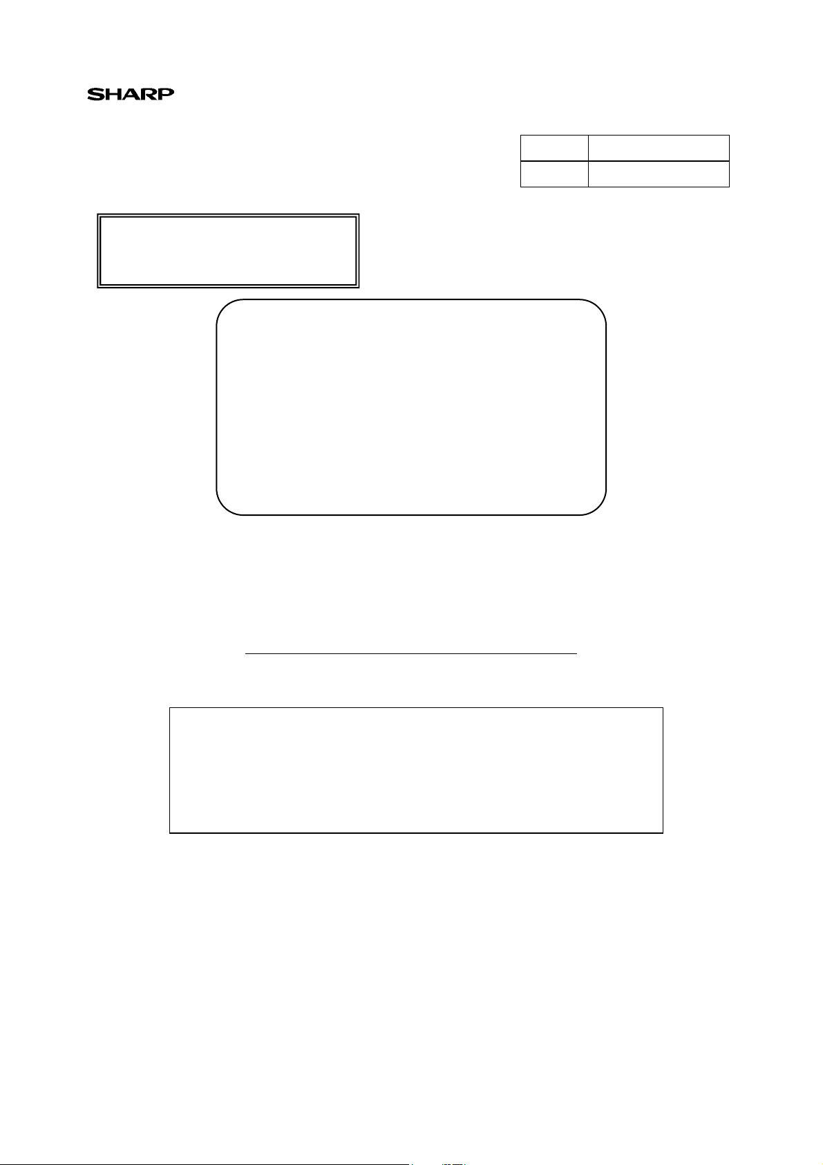
TENTATIVE
TECHNICAL LITERATURE
TFT - LCD module
FOR
No.
DATE Feb. 1, 2010
LD-K22152
MODEL No.
The technical literature is subject to change without notice.
So, please contact SHARP or its representative before designing
your product based on this literature.
LK816D3LA19
MODULE DEVELOPMENT CENTER
AVC LIQUID CRYSTAL DISPLAY GROUP
SHARP CORPORATION
Page 2
LK816D3LA19
RECORDS OF REVISION
SPEC No. DATE
No. PAGE
LD-K22152 Feb. 1, 2010 - - - 1st. Issue
REVISED
SUMMARY NOTE
Page 3
LD-K22152-1
r
1. Application
This technical literature applies to the color 81.6” TFT-LCD module LK816D3LA19.
* These technical literature sheets are proprietary products of SHARP CORPORATION (“SHARP”) and include
materials protected under copyright of SHARP. Do not reproduce or cause any third party to reproduce them in any
form or by any means, electronic or mechanical, for any purpose, in whole or in part, without the express written
permission of SHARP.
* In case of using the device for applications such as control and safety equipment for transportation (aircraft, trains,
automobiles, etc.), rescue and security equipment and various safety related equipment which require higher
reliability and safety, take into consideration that appropriate measures such as fail-safe functions and redundant
system design should be taken.
* Do not use the device for equipment that requires an extreme level of reliability, such as aerospace applications,
telecommunication equipment (trunk lines), nuclear power control equipment and medical or other equipment for
life support.
* SHARP assumes no responsibility for any damage resulting from the use of the device that does not comply with
the instructions and the precautions specified in these technical literature sheets.
* Contact and consult with a SHARP sales representative for any questions about this device.
2. Overview
This module is a color active matrix LCD module incorporating amorphous silicon TFT (T
composed of a color TFT-LCD panel, driver ICs, control circuit, power supply circuit, inverter circuit and back light
system etc. Graphics and texts can be displayed on a 1080×RGB×1920 dots panel with one billion colors by
using LVDS (Low Voltage Differential Signaling) to interface, +12V of DC supply voltages.
This module also includes the DC/AC inverter to drive the CCFT. (+24V of DC supply voltage)
And in order to improve the response time of LCD, this module applies the Over Shoot driving (O/S driving)
technology for the control circuit. In the O/S driving technology, signals are being applied to the liquid crystal
according to a pre-fixed process as an image signal of the present frame when a difference is found between image
signal of the previous frame and that of the current frame after comparing them.
By using the captioned process, the image signals of this LCD module are being set so that image response can be
completed within one frame, as a result, image blur can be improved and clear image performance can be realized.
3. Mechanical Specifications
Paramete
Display size(Diagonal)
Active area 1015.74 (H) x 1805.76 (V) mm
Pixel Format
Pixel pitch 0.9405(H) x 0.9405 (V) mm
Pixel configuration R, G, B horizontal stripe
Display mode Normally black
Unit Outline Dimensions (*1) 1094 (W) x 1879 (H) x 81.9 (D) mm
Mass
Surface treatment
(*1) Outline dimensions are shown in Fig.1.
2071.83 mm
81.5683 inch
1080 (H) x 1920 (V)
(1pixel = R + G + B dot)
64.8±1.0
Anti glare, low reflection coating
Hard coating: 2H
Specifications Unit
hin Film Transistor). It is
pixel
kg
Page 4
4. Input Terminals
4-1. TFT panel driving
CN1 (Interface signals) on CPWB
Using connector : FI-RE51S-VF (Japan Aviation Electronics Industry, Ltd.)
Mating connector : FI-RE51HL (Japan Aviation Electronics Industry, Ltd.)
Mating LVDS transmitter : THC63LVD1023B (THine) or equivalent device
Pin No. Symbol Function Remark
1
2
3
4
5
6
7
8 O/S_SET
9
10
11
12
13
14
15
16
17
18
19
20
21
22
23
24
25
26
27
28
29
30
31
32
33
34
35
36
37
38
39
40
FRAME
Reserved It is required to set non-connection (OPEN).
Reserved It is required to set non-connection (OPEN).
Reserved It is required to set non-connection (OPEN).
TEMP_Error Error output at the ultra high temperature [Note 5]
SELLVDS
INV_duty Inverter Brightness Control [Note 4]
INV_ON/OFF
Frame frequency setting
L: Normal operation
U/D Vertical shift direction [Note 3]
GND
AIN0-
AIN0+
AIN1-
AIN1+
AIN2-
AIN2+
GND
ACK-
ACK+
GND
AIN3-
AIN3+
AIN4-
AIN4+
GND
GND
BIN0-
BIN0+
BIN1-
BIN1+
BIN2-
BIN2+
GND
BCK-
BCK+
GND
BIN3-
BIN3+
BIN4-
H:60Hz, L:50Hz
H: Protection function operates
Select LVDS data order [Note 2]
O/S operation setting
H: O/S driving ON, L: O/S driving OFF
Inverter ON/OFF setting
H:ON, L:OFF
A port (-)LVDS CH0 differential data input
A port (+)LVDS CH0 differential data input
A port (-)LVDS CH1 differential data input
A port (+)LVDS CH1 differential data input
A port (-)LVDS CH2 differential data input
A port (+)LVDS CH2 differential data input
A port LVDS Clock signal(-)
A port LVDS Clock signal(+)
A port (-)LVDS CH3 differential data input
A port (+)LVDS CH3 differential data input
A port (-)LVDS CH4 differential data input
A port (+)LVDS CH4 differential data input
B port (-)LVDS CH0 differential data input
B port (+)LVDS CH0 differential data input
B port (-)LVDS CH1 differential data input
B port (+)LVDS CH1 differential data input
B port (-)LVDS CH2 differential data input
B port (+)LVDS CH2 differential data input
B port LVDS Clock signal(-)
B port LVDS Clock signal(+)
B port (-)LVDS CH3 differential data input
B port (+)LVDS CH3 differential data input
B port (-)LVDS CH4 differential data input
Pull up 3.3V(by 2.0kΩ)
[Note 1]
Pull down GND(by2.0kΩ)
[Note 1]
Pull up 3.3V(by 2.0kΩ)
[Note 1]
Pull up 3.3V(by 2.0kΩ)
[Note 1]
LD-K22152-2
Page 5
41
42
43
44
45
46
47
48
49
50
51
BIN4+ B port (+)LVDS CH4 differential data input
GND
GND
GND
GND
GND
NC
NC
NC
NC
NC
It is required to set non-connection (OPEN).
It is required to set non-connection (OPEN).
It is required to set non-connection (OPEN).
It is required to set non-connection (OPEN).
It is required to set non-connection (OPEN).
* L: Low level voltage (GND). H: High level voltage (3.3V)
*Connect the GND of the liquid crystal panel drive part to the chassis of the module.
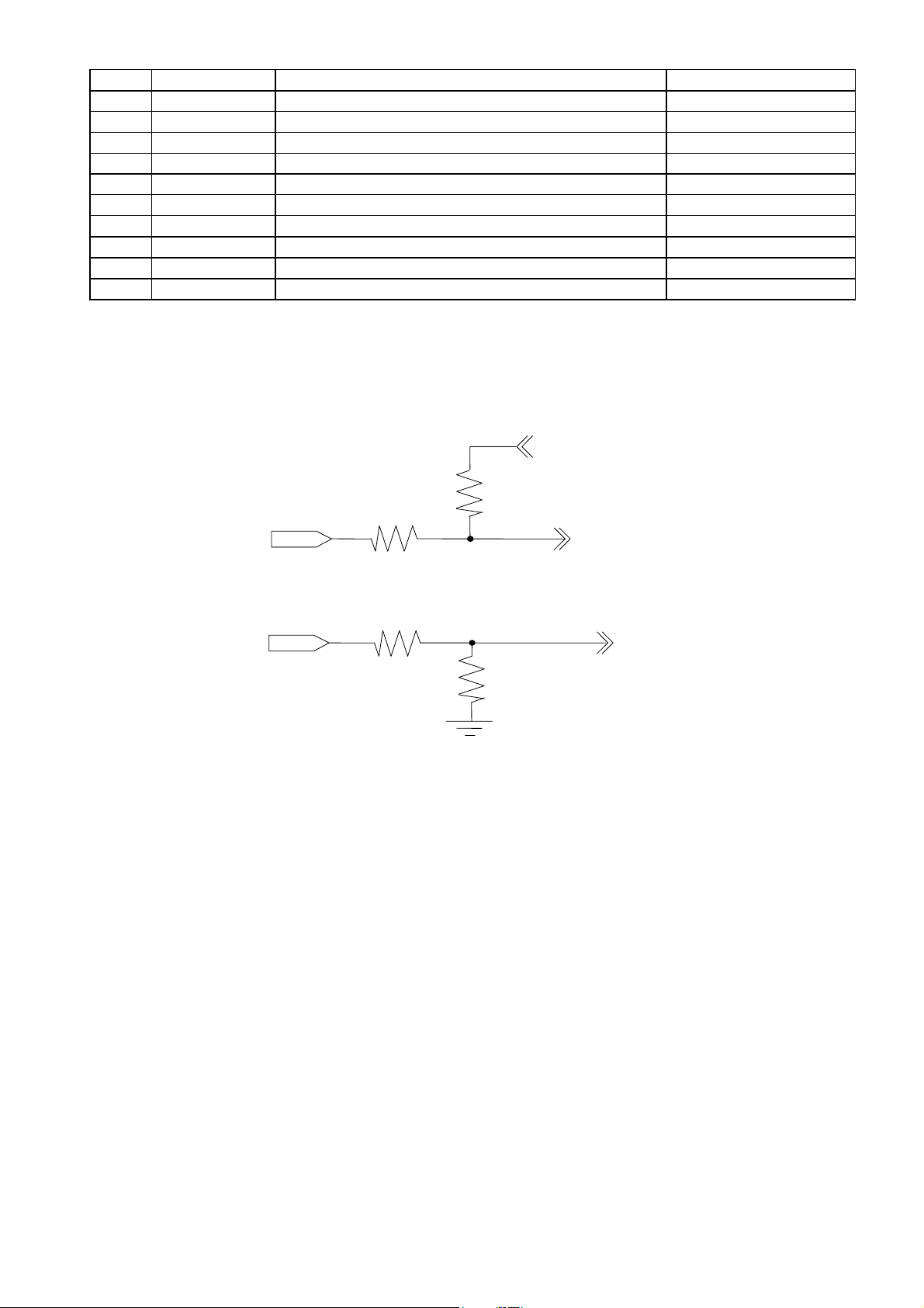
[Note1] The equivalent circuit figure of the terminal
3.3V
FRAME,SELLVDS, O/S_SET
Te rm in al
100Ω
(2.0KΩ)
U/D
Te rm in al
100Ω
(2.0KΩ)
LD-K22152-3
Page 6
[Note2] LVDS data order (SELLVDS=H:JEIDA Mode, L:VESA Mode)
Transmitter
Data
SELLVDS = “L”(GND)
LVDS data
SELLVDS = “H”(3.3V) or Open
LVDS data
TA0 R0(LSB) R4
TA1 R1 R5
TA2 R2 R6
TA3 R3 R7
TA4 R4 R8
TA5 R5 R9(MSB)
TA6 G0(LSB) G4
TB0 G1 G5
TB1 G2 G6
TB2 G3 G7
TB3 G4 G8
TB4 G5 G9(MSB)
TB5 B0(LSB) B4
TB6 B1 B5
TC0 B2 B6
TC1 B3 B7
TC2 B4 B8
TC3 B5 B9(MSB)
TC4 HSYNC HSYNC
TC5 VSYNC VSYNC
TC6 DE DE
TD0 R6 R2
TD1 R7 R3
TD2 G6 G2
TD3 G7 G3
TD4 B6 B2
TD5 B7 B3
TD6 N/A N/A
TE0 R8 R0(LSB)
TE1 R9(MSB) R1
TE2 G8 G0(LSB)
TE3 G9(MSB) G1
TE4 B8 B0(LSB)
TE5 B9(MSB) B1
TE6 N/A N/A
NA: Not Available
*Since the display position is prescribed by the rise of DE (Display Enable) signal,
please do not fix DE signal during operation at “High”.
*HSYNC and VSYNC are not necessary
LD-K22152-4
Page 7
・LVDS da ta order (SELLVDS = “L”)
ACK+, BCK+
ACK-, BCK-
AIN0+, BIN0+
AIN0-, BIN0-
AIN1+,BIN1+
AIN1-,BIN1-
AIN2+,BIN2+
AIN2-,BIN2-
G0 R5 R4 R3 R2 R1 R0 R0 R1 G0
B1 B0 G5 G4 G3 G2 G1 G1 G2 B1
DE
NA
AIN3+,BIN3+
AIN3-,BIN3-
B7 B6 G7 G6 R7 R6 R6 R7 NA NA
AIN4+,BIN4+
AIN4-,BIN4-
B9 B8 G9 G8 R9 R8 R8 R9 NA NA
・LVDS da ta order (SELLVDS = “H”)
ACK+,BCK+
ACK-,BCK-
AIN0+,BIN0+
AIN0-,BIN0-
G4 R9 R8 R7 R6 R5 R4 R4 R5 G4
AIN1+,BIN1+
AIN1-,BIN1-
B5 B4 G9 G8 G7 G6 G5 G5 G6 B5
AIN2+,BIN2+
AIN2-,BIN2-
AIN3+,BIN3+
AIN3-,BIN3-
DE
NA NA
B3 B2 G3 G2 R3 R2 R2 R3 NA NA
AIN4+,BIN4+
AIN4-,BIN4-
B1 B0 G1 G0 R1 R0 R0 R1 NA NA
DE: Display Enable, NA: Not Available (Fixed Low)
NA
1 cycle
B5 B4 B3 B2 B2 B3
1 cycle
B9 B8 B7 B6 B6 B7
LD-K22152-5
DE
DE
Page 8
LD-K22152-6
[Note 3]Display reversal function
Normal (Default)
Vertical reverse image
U/D:L (GND) U/D:H (3.3V)
CONTROL PWB
CONTROL PWB
[Note 4]Brightness Control (Pulse PWM dimming)
Pin No. 9 is used for the control of the PWM duty with input pulse.
T
T
t
t
OFL1/2
duty
Ta = 25°C
MIN TYP MAX Remark
Pulse signal [Hz] 155 165 175
DUTY (t/T) [%] 20
-
100
*There is a case that lamp mura may happen, depending on ambient temperature, in
dimming. Minimum dimming level should be set according to your evaluation of actual
display performance. (Minimum duty 60% at below 15℃)
[Note 5] Error output at the ultra high temperature
For the protection of the module C_PWB decreases DUTY of PWM of the inverter to 30% forcibly when the
temperature of the module is more than (85) ℃. Duty of PWM of the inverter returns to a normal state
afterwards when the temperature of the module is less than (55) ℃.
Error output is Low (0V) at normal state. Error output becomes High (3.3V) when protection function operates.
Page 9

LD-K22152-7
R
R
R
CN2 (+12V DC power supply) on CONTROL PWB
Using connector : SM04B-PASS-TBT (J.S.T. Mfg Co., Ltd.)
Mating connector : PAP-04V-S (J.S.T. Mfg Co., Ltd.)
Pin No.
1 VCC
2 VCC
3 GND
4 GND
Symbol Function Remark
+12V Power Supply
+12V Power Supply
GND
GND
*Current rating:3A (AWG#22)
Block Diagram (LCD Module)
INPUT SIGNALS
INV_duty, INV_ON/OFF, O/S_SET, SELLVDS,
・
FRAME,
AIN0-, AIN0+, AIN1-, AIN1+, AIN2-, AIN2+
AIN3-, AIN3+, AIN4-, AIN4+, ACK-, ACK+、
BIN0-, BIN0+, BIN1-, BIN1+, BIN2-, BIN2+
BIN3-, BIN3+, BIN4-, BIN4+, BCK-, BCK+
OUTPUT SIGNALS
TEMP_Error
CN1
GATE DRIVE
BACK LIGHT(120 CCFTs )
LCD PANEL
1080X1920
POWER SUPPLY
+24V DC
GND
POWER SUPPLY
CONTROL PWB
+12V DC
GND
CN2
SOURCE DRIVE
GATE DRIVE
INVERTER PWB
CN3 ,4 ,5 ,6 ,7 ,8 CN,9,10,11,12,13,14
Page 10

0
0
A
0
0
0
L
L
0
0
9 AB0AB
9
LCD
I
l
Ci
i
A
A
A
A
A
A
A
A
A
BB9
0
0
0
0
LPLL
0
0
0
BG0 BG9 CLK
B
A
B AIN4+(25
BIN4–(
B
Interface block diagram
AG
AB
AR
AR9
AG9
AB9
Con t r o l l e r
ENAB_
Hsy n c _ A
Vsync_ A
CLKA
BR
BR9
BG0 BG9
BB0
ENAB_ B
Hs yn c_
Vs yn c_ B
CLKB
Corresponding Transmitter:
LD-K22152-8
(TV Side)
Port A
1
10
1
LVDS
TTL
PL
Port B
1
1
1
LVDS
TTL
PLL
IN0+(13)
IN0– (12)
IN1+(15)
IN1– (14)
IN2+(17)
IN2– (16)
IN3+(23)
IN3– (22)
AIN4– (24)
ACK+( 2 0)
CK– (19)
BIN0+(29)
BIN0– (28)
BIN1+(31)
BIN1– (30)
BIN2+(33)
BIN2– (32)
BIN3+(39)
BIN3– (38)
BIN4+(41)
BCK+( 36 )
BCK–(3 5)
(TFT-LCD side)
Port
TT
LVDS
)
PLL
Por t
TT
LVDS
40)
1
AR0AR
1
AG0AG9
10
1
BR0 BR9
1
1
BB0 BB9
DE_ A
Hsy nc _ A
Vsync_ A
CLKA
DE_B
Hsync_ B
Vs yn c_ B
t
rcu
nterna
THC63LVD1023B (THine) or equivalent device
Page 11

LD-K22152-9
4-2. Backlight driving
Inverter connecter1 (+24V DC power supply and inverter control)
CN3, CN4, CN5, CN6, CN7, CN8 (Inverter Power input Pin layout) on INVERTER PWB
Using connector: S14B-PH-K-S (LF) (J.S.T. Mfg Co.,Ltd.)
Mating connector: PHR-14 (J.S.T. Mfg Co.,Ltd.)
Pin No. Symbol Function Remark
1 VINV +24V
2 VINV +24V
3 VINV +24V
4 VINV +24V
5 VINV +24V
6 GND GND
7 GND GND
8 GND GND
9 GND GND
10 GND GND
11 Reserved It is required to set non-connection (OPEN).
12 Reserved It is required to set non-connection (OPEN).
13 Reserved It is required to set non-connection (OPEN).
14 Reserved It is required to set non-connection (OPEN).
*Current rating:2A (AWG#24)
Inverter connecter2 (+24V DC power supply)
CN9, CN10, CN11, CN12, CN13, CN14 (Inverter Power input Pin layout) on INVERTER PWB
Using connector : S12B-PH-K-S(LF) (J.S.T. Mfg Co.,Ltd.)
Mating connector : PHR-12 (J.S.T. Mfg Co.,Ltd.)
Pin No. Symbol Function
1 VINV +24V
2 VINV +24V
3 VINV +24V
4 VINV +24V
5 VINV +24V
6 GND GND
7 GND GND
8 GND GND
9 GND GND
10 GND GND
11 Reserved It is required to set non-connection (OPEN)
12 Reserved It is required to set non-connection (OPEN)
*Current rating:2A (AWG#24)
4-3. the back light system characteristics
The back light system is direct type with 120 CCFTs (Cold Cathode Fluorescent Tube).
The characteristics of the lamp are shown in the following table.
The value mentioned below is at the case of one CCFT.
Item Symbol Min. Typ. Max. Unit Remarks
Life time TL - (60000) - Hour
[Note]・Lamp life time is defined as the time when brightness becomes 50% of the original value
in the continuous operation under the condition the Ta=25 ℃ and brightness control(duty=100%).
・Above value is applicable when the long side of LCD module is placed vertically (Portrait position).
Page 12

5. Absolute Maximum Ratings
Parameter Symbol Condition Ratings Unit Remark
Input voltage
(for Control)
12V supply voltage
(for Control)
24V supply voltage
(for Inverter)
LD-K22152-10
I
V
Ta=25 ℃
-0.3 ~ 3.6 V [Note 1]
VCC Ta=25 ℃ 0 ~ + 14 V
V
INV
Ta=25 ℃
0 ~ +27 V
Storage temperature Tstg - -25~ +60
Operation temperature
(Ambient) Topa - 0 ~ +35
℃
℃
[Note 2]
[Note 3]
[Note 4]
[Note 5]
[Note 1] FRAME, SELLVDS, O/S_SET, U/D,INV_duty,INV_ON/OFF
[Note 2] Humidity 95%RH Max.(Ta≦40℃)
Maximum wet-bulb temperature at 39 ℃ or less.(Ta>40 ℃) / No condensation.
[Note 3] Temperature Uniformity :10 ℃ Max.
[Note 4] Glass surface temperature : 55 ℃ Max,
[Note 5] To put out high brightness a lot of lamps are built into this module. Therefore, when this module is
operated, cooling this module is required. There is a possibility of damaging the module when a
surrounding operating temperature is exceeded.
Page 13

LD-K22152-11
,
V
6. Electrical Characteristics
6-1. Control circuit driving Ta=25 ℃
Parameter Symbol Min. Typ. Max. Unit Remark
Supply voltage Vcc 11.4 12.0 12.6
V
[Note1]
+12V supply
voltage
Current dissipation Icc - (0.9) (1.5) A [Note2]
1 -
I
RUSH
(TBD)
- A
Inrush current
I
2 -
RUSH
(TBD)
- A t1>5ms
Permissible input ripple voltage VRP - - 100 mVP-P Vcc = +12.0V
Input Low voltage VIL 0 - 0.8 V
Input High voltage VIH 2.3 - 3.6 V
Input leak current (Low) IIL - - 400 µA VI = 0V
Input leak current (High) IIH 100 µA VI=3.3V
Termin al resistor RT - 100 -
Ω
Input Differential Voltage |VID| 200 400 600 mV [Note3]
Differential Input common mode
voltage
VCM |VID|/2 1.2 2.4-|VID|/2 V
[Note]VCM: Common mode voltage of LVDS driver.
[Note 1]
Input voltage sequences Dip conditions for supply voltage
0.1 ms < t1 ≦ 20 ms a) 6.5V ≦ Vcc < 10.8V
10 ms < t2 ≦ 50 ms td ≦ 10 ms
10 ms < t3 ≦ 50 ms b) Vcc < 6.5 V
0 ms < t4 ≦ 1 s Dip conditions for supply voltage is
t5 ≧ 1 s based on input voltage sequence.
t6 ≧ 0
t7 ≧ 1 s
t8 ≧ 500 ms
t9 ≧ 1 s
t1=500us
[Note4]
Differential input
[Note3]
Data1
Data2
Back light:
INV
Back light:
V
cc
INV
on/off
0.1Vcc
INVduty
0.9 Vcc
t1
t2
t3
t8
0.9 Vcc
0.1Vcc
t4
ON
t3
t5
OFF
t6
OFF
0.1Vcc
0.1Vcc
t7
td
0.1Vcc
t9
Data1:ACK±,AIN0±,AIN1±, AIN2±, AIN3±, AIN4±, BCK±,BIN0±,BIN1±, BIN2±, BIN3±, BIN4±
Data2:SELLVDS, FRAME, O/S_SET,
V2
Vcc
V1
V1: 10.8V
V2: 6.5V
Page 14

LD-K22152-12
*About the relation between data input and back light lighting, please base on the above-mentioned input
sequence. When back light is switched on before panel operation or after a panel operation stop, it may not
display normally. But this phenomenon is not based on change of an incoming signal, and does not give
damage to a liquid crystal display.
[Note 2] Typical current situation: 1024 gray-bar patterns. (Vcc = +12.0V)
The explanation of RGB gray scale is seen in section 8.
RGB
GS1023
RGB
GS1022
....
Vcc=12.0V
CK=74.25MHz
TT=14.8μs
RGB
GS2
RGB
GS1
RGB
GS0
[Note3] ACK±,BCK±,AIN0±,AIN1±,AIN2±,AIN3±, AIN4±,BIN0±,BIN1±,BIN2±,BIN3±, BIN4±
*CK-,*IN-
*CK+,*IN+
GND
|VID|
|VID|
VCM
[Note4] SELLVDS, FRAME, O/S_SET, U/D, INV_duty,INV_ON/OFF
Page 15

LD-K22152-13
V
V
3
1
V
V
6-2. Inverter driving for back light
The back light system is
direct type with 120CCFTs (Cold Cathode Fluorescent Tube). Ta=25℃
Parameter Symbol Min. Typ. Max. Unit Remark
INV_ON/OFF=3.3V
Supply voltage VINV 23.0 24.0 25.0 V
Current dissipation1 IINV1
+24V
Current dissipation2 IINV 2
Permissible input ripple
voltage
Input voltage (Low) V
Input voltage (High) V
- (62) (70) A
- (TBD) (TBD) A
- (50) (58) A
- (65) (75) A
RF - - 300 mV
V
0 - 0.8 V
ONL
2.3 3.3 3.6 V
ONH
INV_duty = 100%
【Note1】【Note2】
VINV = 24V
INV_ON/OFF=3.3V
INV_duty = 100%
【Note1】【Note2】
VINV = 24V
INV_ON/OFF=3.3V
INV_duty = 100%
※with cooling module
【Note1】【Note2】
VINV = 24V
INV_ON/OFF=3.3V
INV_duty = 100%
【Note1】【Note2】
VINV = 24V
INV_ON/OFF=3.3V
INV_duty = 100%
※with cooling module
【Note1】【Note2】
VINV = 24V
p-p
INV_ON/OFF, INV_duty
【Note1】
【Note 1】1)VINV-turn-on condition
CC( CONTROL PWB)
0.9VCC
T1
T2
0.9VINV
T1≧500ms
T2>100s
≧1ms
T
INV
0V
0.1VINV
T3
_ON/OFF,
_on/off,
INV_duty
INV_duty
t1
0.
INVON/O FF
t1≧1ms
t2≧1ms
INV
2) V
INV-turn-off condition
INV
INV
CC(CONTROL
0.8V
PWB)
t2
0.9V
0.9V
0V
INV
0V
INV
0V
【Note 2】Current dissipation1 : Definition within 120 minutes after turn on.( Rush current Is excluded)
Current dissipation2 : Definition more than 120 minutes after turn on.
【Note】 The inverter unit is driving at the following drive frequency.
*The lamp drive frequency : 31.4 ±2.0 kHz
*The burst Brightness control drive frequency : 165 ± 10 Hz
Page 16

LD-K22152-14
r
7. Timing characteristics of input signals
7-1. Timing characteristics
This LCD module is designed to be used in portrait position other than input signal.
The definition of input signal is based on landscape position. Therefore, please ensure to take it into account in
designing your set.
Timing diagrams of input signal are shown in Fig.2.
Paramete
Symbol Min. Typ. Max. Unit Remark
Clock Frequency 1/Tc 69 74.25 76 MHz
1084 1100 1200 clock
14.6 14.8 16.1 µs
1109 1125 (1400) line
47 60 63 Hz
Data enable
signal
Horizontal period TH
Horizontal period (High) THd 960 960 960 clock
Vertical period
TV
Vertical period (High) TVd 1080 1080 1080 line
【Note】*When vertical period is very long, flicker and others may occur.
*Please turn off the module after it shows the black screen.
*Please make sure that length of vertical period should become of an integral multiple
of horizontal length of period. Otherwise, the screen may not display properly.
*As for your final setting of driving timing, we will conduct operation check test at our side,
please inform your final setting.
TH
THd
DE
A port data
1919
1
3
1919
(R, G, B)
B port data
2
4 1920 1920
(R, G, B)
Tc
1 2
1079
1080
DE
TV
TVd
Fig.2 Timing characteristics of input signals
Page 17

7-2. Input data signal and display position on the screen
G
LD-K22152-15
1・1920
CONTROL PWB
Direction of H
B2
G2
R2
B1
G1
R1
( 1,2 )
B port
( 1,1 )
A port
1・3
1・2
1・1
2・2
2・1
Dire ction of V
1080・1920
B
R
1080・1
3・1
Display position of data (V,H)
Page 18

LD-K22152-16
8. Input Signal, Basic Display Colors and Gray Scale of Each Color
Colors &
Gray
scale
Black – 0 0 0 0 0 0 0 0 0 0 0 0 0 0 0 0 0 0 0 0 0 0 0 0 0 0 0 0 0 0
Blue – 0 0 0 0 0 0 0 0 0 0 0 0 0 0 0 0 0 0 0 0 1 1 1 1 1 1 1 1 1 1
Green – 0 0 0 0 0 0 0 0 0 0 1 1 1 1 1 1 1 1 1 1 0 0 0 0 0 0 0 0 0 0
Cyan – 0 0 0 0 0 0 0 0 0 0 1 1 1 1 1 1 1 1 1 1 1 1 1 1 1 1 1 1 1 1
Red – 1 1 1 1 1 1 1 1 1 1 0 0 0 0 0 0 0 0 0 0 0 0 0 0 0 0 0 0 0 0
Basic Color
Magenta – 1 1 1 1 1 1 1 1 1 1 0 0 0 0 0 0 0 0 0 0 1 1 1 1 1 1 1 1 1 1
Yellow – 1 1 1 1 1 1 1 1 1 1 1 1 1 1 1 1 1 1 1 1 0 0 0 0 0 0 0 0 0 0
White – 1 1 1 1 1 1 1 1 1 1 1 1 1 1 1 1 1 1 1 1 1 1 1 1 1 1 1 1 1 1
Black GS0 0 0 0 0 0 0 0 0 0 0 0 0 0 0 0 0 0 0 0 0 0 0 0 0 0 0 0 0 0 0
Gray
R0 R1 R2 R3 R4 R5 R6 R7 R8 R9 G0 G1 G2 G3 G4 G5 G6 G7 G8 G9 B0 B1 B2 B3 B4 B5 B6 B7 B8 B9
Scale
GS1 1 0 0 0 0 0 0 0 0 0 0 0 0 0 0 0 0 0 0 0 0 0 0 0 0 0 0 0 0 0
Darker GS2 0 1 0 0 0 0 0 0 0 0 0 0 0 0 0 0 0 0 0 0 0 0 0 0 0 0 0 0 0 0
Brighter GS1021 1 0 1 1 1 1 1 1 1 1 0 0 0 0 0 0 0 0 0 0 0 0 0 0 0 0 0 0 0 0
Data signal
Gray Scale of Red
GS1022 0 1 1 1 1 1 1 1 1 1 0 0 0 0 0 0 0 0 0 0 0 0 0 0 0 0 0 0 0 0
Red GS1023 1 1 1 1 1 1 1 1 1 1 0 0 0 0 0 0 0 0 0 0 0 0 0 0 0 0 0 0 0 0
Black GS0 0 0 0 0 0 0 0 0 0 0 0 0 0 0 0 0 0 0 0 0 0 0 0 0 0 0 0 0 0 0
GS1 0 0 0 0 0 0 0 0 0 0 1 0 0 0 0 0 0 0 0 0 0 0 0 0 0 0 0 0 0 0
Darker GS2 0 0 0 0 0 0 0 0 0 0 0 1 0 0 0 0 0 0 0 0 0 0 0 0 0 0 0 0 0 0
Brighter GS1021 0 0 0 0 0 0 0 0 0 0 1 0 1 1 1 1 1 1 1 1 0 0 0 0 0 0 0 0 0 0
Gray Scale of Green
GS1022 0 0 0 0 0 0 0 0 0 0 0 1 1 1 1 1 1 0 0 1 0 0 0 0 0 0 0 0 0 0
Green GS1023 0 0 0 0 0 0 0 0 0 0 1 1 1 1 1 1 1 1 1 1 0 0 0 0 0 0 0 0 0
Black GS0 0 0 0 0 0 0 0 0 0 0 0 0 0 0 0 0 0 0 0 0 0 0 0 0 0 0 0 0 0 0
GS1 0 0 0 0 0 0 0 0 0 0 0 0 0 0 0 0 0 0 0 0 1 0 0 0 0 0 0 0 0 0
Darker GS2 0 0 0 0 0 0 0 0 0 0 0 0 0 0 0 0 0 0 0 0 0 1 0 0 0 0 0 0 0 0
Brighter GS1021 0 0 0 0 0 0 0 0 0 0 0 0 0 0 0 0 0 0 0 0 1 0 1 1 1 1 1 1 1 1
Gray Scale of Blue
GS1022 0 0 0 0 0 0 0 0 0 0 0 0 0 0 0 0 0 0 0 0 0 1 1 1 1 1 1 1 1 1
Blue GS1023 0 0 0 0 0 0 0 0 0 0 0 0 0 0 0 0 0 0 0 0 1 1 1 1 1 1 1 1 1 1
0: Low level voltage, 1: High level voltage.
Each basic color can be displayed in 1021 gray scales from 10 bit data signals. According to the combination of
total 30 bit data signals, the one billion-color display can be achieved on the screen.
Page 19

LD-K22152-17
p
9. Optical characteristics
Vcc = 12.0V, V
INV = 24.0V, Timing:60Hz, Ta=25℃(typ. Value)
Parameter Symbol Condition Min. Typ. Max. Unit Remark
Viewing angle
Horizontal
range
Vertical
Contrast ratio CRn
Response time
θ21
θ22
θ11
θ12
τDRV
CR≧10
70 88 - Deg.
[Note1][Note4]
70 88 - Deg.
(950) (1500) -
INV
[Note2][Note4]
INV
- (6) - ms
[Note3][Note4]
_duty
_duty
=100%
=100%
[Note5]
Chromaticity of white
Chromaticity of red
Chromaticity of green
Chromaticity of blue
Luminance of white YL1
x
y
x
y
x
θ=0 deg
y
x
y
0.257 0.287 0.317
0.265 0.295 0.325
0.564 0.594 0.624
0.302 0.332 0.362
0.259 0.289 0.319
0.531 0.561 0.591
0.117 0.147 0.177
0.066 0.096 0.126
(800) (1200) -
1200 1500 -
-
-
-
-
-
-
-
-
cd/m2
INV_
=100%
duty
[Note 4]
INV
=100%
_duty
[Note 4]
INV
_duty
=100%
with cooling module
[Note 4][Note7]
Luminance uniformity δW - - (1.25) [Note 6]
Measurement condition: Set the value of duty to maximum luminance of white.
*The measurement shall be executed 120 minutes after lighting at rating.
【Note】The optical characteristics are measured using the following equipment.
Detector(EZ-CONTRAST/Photo Diode)
2500 mm
Detector(SR-3)
Field=1°
Middle of the screen (θ=0°)
Middle of the screen (θ=0°)
TFT-LCD Module
TFT-LCD Module
Fig.3-1 Measurement of viewing angle range
and response time.
Fig.3-2 Measurement of Contrast, Luminance,Chromaticity .
Viewing angle range : EZ-CONTRAST
onse time : Photo Diode
Res
Page 20

LD-K22152-18
[Note 1]Definitions of viewing angle range:
Normal
θ11
θ22
θ21
θ12
6 o’clock direction
[Note 2]Definition of contrast ratio:
The contrast ratio is defined as the following.
Luminance (brightness) with all pixels white
Contrast Ratio
=
Luminance (brightness) with all pixels black
[Note 3]Definition of response time
The response time (
) is defined as the following figure and shall be measured by switching the input
Drv
signal for “five luminance ratio (0%, 25%, 50%, 75%, and 100%)” and “five luminance ratio (0%, 25%, 50%,
75%, and 100%)”.
0% 25% 50% 75% 100%
0% tr: 0%-25% tr: 0%-50% tr: 0%-75% tr: 0%-100%
25% td: 25%-0% tr: 25%-50% tr: 25%-75% tr: 25%-100%
50% td: 50%-0% td: 50%-25% tr: 50%-75% tr: 50%-100%
75% td: 75%-0% td: 75%-25% td: 75%-50% tr: 75%-100%
100% td: 100%-0% td: 100%-25% td: 100%-50% td: 100%-75%
t*: x-y...response time from level of gray(x) to level of gray(y)
= (t*: x-y)/20
Drv
[Note 4]This shall be measured at center of the screen.
[Note 5] Response time is the value when O/S driving is used at typical input time value.
[Note 6]Definition of white uniformity;
White uniformity is defined as the following with five measurements. (A~E)
E
Pixel
1440
960
Maximum luminance of five points (brightness)
W=
δ
Minimum luminance of five points (brightness)
270 540 810
D
C
A B
480
Pixel
Page 21

LD-K22152-19
[Note 7] Fig.4 shows relation between the temperature of blowing air in the thermostatic chamber and luminance of
white and relation between the temperature of blowing air in the thermostatic chamber and power.
㏅/㎡
Luminance of white
1800
1600
1400
1200
1000
0 10203035
Environmental temperature
℃
Fig.4 the temperature of blowing air in thermostatic chamber
(TBD)
10. Handling Precautions of the module
a) Be sure to turn off the power supply when inserting or disconnecting the cable.
b) This product is using the parts (inverter, CCFT etc), which generate the high voltage.
Therefore, during operating, please don't touch these parts.
c) Brightness control voltage is switched for “ON” and “OFF”, as shown in Fig.5. Voltage difference generated
by this switching, ΔV
INV, may affect a sound output, etc. When the power supply is shared between the
inverter and its surrounding circuit. So, separate the power supply of the inverter circuit with the one of its
surrounding circuit.
ΔVINV
VINV
IINV
PWM control
signal
0V
0A
ON ON OFF
0V
Fig.5 Brightness control voltage.
d) Be sure to design the cabinet so that the module can be installed without any extra stress such as warp or
twist.
e) Since the front polarizer is easily damaged, pay attention not to scratch it.
f) Since long contact with water may cause discoloration or spots, wipe off water drop immediately.
g) When the panel surface is soiled, wipe it with absorbent cotton or other soft cloth.
Page 22

LD-K22152-20
h) Since the panel is made of glass, it may break or crack if dropped or bumped on hard surface. Handle with
care.
i) Since CMOS LSI is used in this module, take care of static electricity and take the human earth into
consideration when handling.
j) The module has some printed circuit boards (PCBs) on the back side, take care to keep them from any stress
or pressure when handling or installing the module; otherwise some of electronic parts on the PCBs may be
damaged.
k) Observe all other precautionary requirements in handling components.
l) When some pressure is added onto the module from rear side constantly, it causes display non-uniformity
issue, functional defect, etc... So, please avoid such design.
m) When giving a touch to the panel at power on supply, it may cause some kinds of degradation. In that case,
once turn off the power supply, and turn on after several seconds again, and that is disappear.
n) When handling LCD modules and assembling them into cabinets, please be noted that long-term storage in
the environment of oxidization or deoxidization gas and the use of such materials as reagent, solvent,
adhesive, resin, etc. which generate these gasses, may cause corrosion and discoloration of the LCD
modules.
o) Lamps of the backlight are placed horizontally to the short side of LCD module. The lifetime of the backlight
shortens if the module is used in landscape position.
p) Make sure that the LCD module is operated within specified temperature and humidity.
Measures against dust, water, vibration, and heat radiation, etc. are required at the cabinet or equipment side.
And image retention may occur if same fixed pattern is displayed for a long time.
In some cases, it may not disappear. It is recommended to use moving picture periodically.
After long-term static display, periodical power-off or screen saver is needed. For screen saver,
moving picture or black pattern is strongly recommended.
Avoid combination of background and image with large different luminance.
Please consider the design and operating environment.
q) Ultra-violet ray filter is necessary in outdoor environment.
r) Operation for 24 hours a day is NOT recommended.
s) Well-ventilated place is recommended to set up Information Display system.
t) Execute it at 0℃ or above when you light the module. There is a possibility of don't lighting when begin
lighting at a temperature that is lower than 0℃
u) If you control the temperature of the ambient air or the module, please equalize the temperature
of the module.
Page 23

11. Packing form
2
a) Piling number of cartons: 1 maximum. (Do not pile up.)
b) Packing quantity in one carton: 4 pcs.
c) Carton size: (1230) (W) × (1090) (D) × (2134) (H)
d) Total mass of one carton filled with full modules: (TBD)kg
e) Packing Form is shown in Fig 5. (TBD)
12. Reliability test item *only as for the module.
No. Test item Condition
High temperature storage test
1
Low temperature storage test
2
High temperature and high humidity
3
operation test
High temperature operation test
4
Low temperature operation test
5
Vibration test*
(non-operation)
6
Ta=60℃ 240h
Ta=-20℃ 240h
Ta=40℃ ; 95%RH 240h
(No condensation)
Ta=40℃ 240h
Ta= 0℃ 240h
Frequency: 10~57Hz/Vibration width (one side): 0.075mm
: 58~500Hz/Acceleration: 9.8 m/s
Sweep time: 11 minutes
Test period: 1.5 hours (0.5h for each direction of X, Y, Z)
Shock test*
7
(non-operation)
Maximum acceleration: 294m/s
Pulse width: 11ms, sinusoidal half wave
Direction: (+/-Y), once for each direction.
At the following conditions, it is a thing without incorrect
operation and destruction.
(1)Non-operation: Contact electric discharge +/-10kV
ESD
8
Non-contact electric discharge+/-20kV
(2)Operation Contact electric discharge +/-8kV
Non-contact electric discharge +/-15kV
Conditions: 150Pf,330ohm
【Note】these items apply to the single module.
【Result evaluation criteria】
Under the display quality test condition with normal operation state, there shall be no change, which may
affect practical display function.
LD-K22152-21
2
Page 24

LD-K22152-22
(
)
13. Others
1) Lot No. Label
The label that displays SHARP, product model (LK816D3LA19), a product number is stuck on the
back of the module.
LK816D3LA19
01 L50 001
MADE IN JAPAN
Module No.
Barcode
ot No.
A production year (the last figures of the Christian era)
A production month (1-9, X,Y, Z)
Identification Code
L:Kameyama Tec. Kameyama Fab.
How to express Lot No.
○ L ○ ○ ○ ○ ○ ○○
○
Serial number
Management number
2) Packing Label
社内品番:
Bar code(①)
LotNO.
Bar code(②)
Quantity:
Bar code(③)
ユーザ品番
シャープ物流用ラベルです。
4S
LK816D3LA19
(1T)201*. *.**
(Q)
pcs
4
① Management No. (LK816D3LA19)
② Lot No. (Date)
③ Quantity
3) Adjusting volume has been set optimally before shipment, so do not change any adjusted value.
If adjusted value is changed, the specification may not be satisfied.
4) Disassembling the module can cause permanent damage and should be strictly avoided.
5) Please be careful since image retention may occur when a fixed pattern is displayed for a long time.
6) The chemical compound, which causes the destruction of ozone layer, is not being used.
7) Cold cathode fluorescent lamp in LCD PANEL contains a small amount of mercury. Please follow local
ordinances or regulations for disposal. It is displaying the label in the module back.
Page 25

LD-K22152-23
8) This LCD is appropriate to UL. Below figure shows the UL label.
9) This module is corresponded to RoHS
10) The chemical compound, which causes the destruction of ozone layer, is not being used.
11) Rust on the module is not taken up a problem.
12) Appearance quality and standard are referred to the outgoing incoming inspections.
13) Rust on the module is not taken up a problem.
14. Carton storage condition
Temperature 0℃ to 40℃
Humidity 95%RH or less
Reference condition : 20℃ to 35℃ , 85%RH or less (summer)
: 5℃ to 15℃ , 85%RH or less (winter)
・the total storage time (40℃,95%RH) : 240h or less
Sunlight Be sure to shelter a product from the direct sunlight.
Atmosphere Harmful gas, such as acid and alkali which bites electronic components and/or
wires must not be detected.
Notes Be sure to put cartons on palette or base, don’t put it on floor, and store them with
removing from wall
Please take care of ventilation in storehouse and around cartons, and control
changing temperature is within limits of natural environment
Please keep LCD module in Portrait position.
(The long side of LCD module is placed vertically)
Storage life 1 year
Factory code
Page 26

ᾛᾓὼᾚᾁᾁᾀᾄᾁὼᾁᾃ
ᾕᶇᶅᵋᵏ
 Loading...