

Page 1
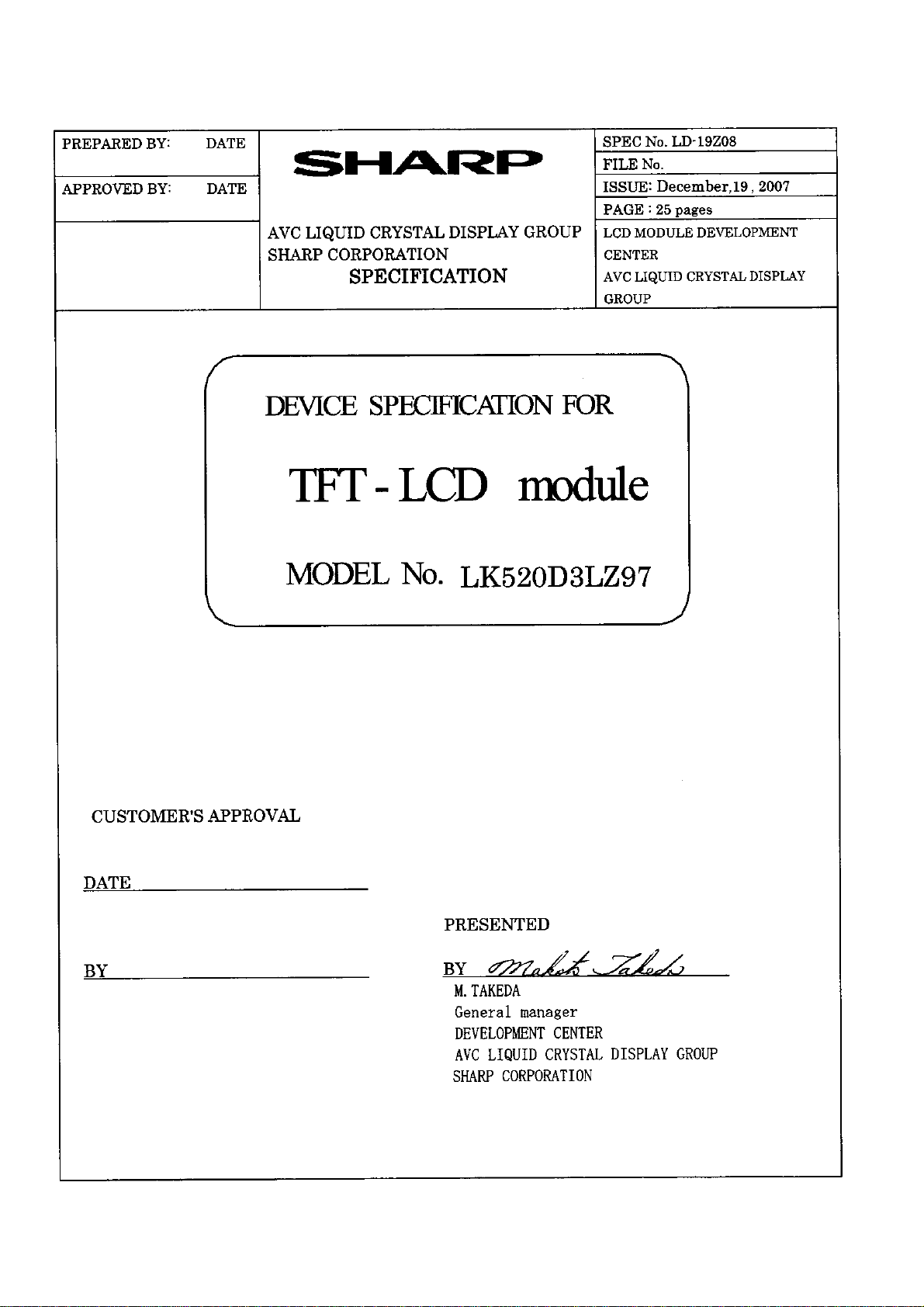
26
Page 2
Page 3
LD- 19Z08-1
1. Application
This specification applies to the color 52.0” TFT-LCD module LK520D3LZ97.
* These specification are proprietary products of SHARP CORPORATION (“SHARP”) and include materials
protected under copyright of SHARP. Do not reproduce or cause any third party to reproduce them in any form or by
any means, electronic or mechanical, for any purpose, in whole or in part, without the express written permission of
SHARP.
* In case of using the device for applications such as control and safety equipment for transportation (aircraft, trains,
automobiles, etc.), rescue and security equipment and various safety related equipment which require higher
reliability and safety, take into consideration that appropriate measures such as fail-safe functions and redundant
system design should be taken.
* Do not use the device for equipment that requires an extreme level of reliability, such as aerospace applications,
telecommunication equipment (trunk lines), nuclear power control equipment and medical or other equipment for
life support.
* SHARP assumes no responsibility for any damage resulting from the use of the device that does not comply with
the instructions and the precautions specified in these specification.
* Contact and consult with a SHARP sales representative for any questions about this device.
2. Overview
This module is a color active matrix LCD module incorporating amorphous silicon TFT (Thin Film Transistor). It is
composed of a color TFT-LCD panel, driver ICs, control circuit, power supply circuit, inverter circuit and back light
system etc. Graphics and texts can be displayed on a 1920×RGB×1080 dots panel with
using LVDS (L
This module also includes the DC/AC inverter to drive the CCFT. (+24V of DC supply voltage)
And in order to improve the response time of LCD, this module applies the Over Shoot driving (O/S driving)
technology for the control circuit .In the O/S driving technology, signals are being applied to the Liquid Crystal
according to a pre-fixed process as an image signal of the present frame when a difference is found between image
signal of the previous frame and that of the current frame after comparing them.
With this technology, image signals can be set so that liquid crystal response completes within one frame. As a
result, motion blur reduces and clearer display performance can be realized.
This LCD module also adopts Double Frame Rate driving method.
With combination of these technologies, motion blur can be reduced and clearer display performance can be
realized.
ow Voltage Differential Signaling) to interface, +12V of DC supply voltages.
one billion
colors by
3. Mechanical Specifications
Parameter Specifications Unit
Display size
Active area 1152.0(H) x 648.0 (V) mm
Pixel Format
Pixel pitch 0.600(H) x 0.600 (V) mm
Pixel configuration R, G, B vertical stripe
Display mode Normally black
Unit Outline Dimensions (*1) 1219.0(W) x 706.7(H) x 64.6(D) mm
Mass
Surface treatment
(*1) Outline dimensions are shown in Fig.1 (excluding protruding portion)
132.174 (Diagonal)
52.0 (Diagonal)
1920(H) x 1080(V)
(1pixel = R + G + B dot)
21.0 ±1.0
Anti glare
Hard coating: 2H
cm
inch
pixel
kg
Page 4
4. Input Terminals
4.1. TFT panel driving
CN1 (Interface signals and +12V DC power supply) (Shown in Fig.1)
Using connector : FI-RE51S-HF (Japan Aviation Electronics Ind., Ltd.)
Mating connector : FI-RE51HL, FI-RE51CL (Japan Aviation Electronics Ind., Ltd.)
Mating LVDS transmitter : THC63LVD1023 or equivalent device
Pin No. Symbol Function Remark
1
2
3
4
5
6
7
8
9
10
11
12
13
14
15
16
17
18
19
20
21
22
23
24
25
26
27
28
29
30
31
32
33
34
35
36
37
38
39
40
41
42
43
44
GND
Reserved It is required to set non-connection(OPEN)
Reserved It is required to set non-connection(OPEN)
Reserved It is required to set non-connection(OPEN)
FRAME
O/S set O/S operation setting H:O/S_ON, L:O/S_OFF [Note 3] Pull up 3.3V
SELLVDS
Reserved
Reserved
Reserved
GND
AIN0- Aport (-)LVDS CH0 differential data input
AIN0+ Aport (+)LVDS CH0 differential data input
AIN1- Aport (-)LVDS CH1 differential data input
AIN1+ Aport (+)LVDS CH1 differential data input
AIN2- Aport (-)LVDS CH2 differential data input
AIN2+ Aport (+)LVDS CH2 differential data input
GND
ACK- Aport LVDS Clock signal(-)
ACK+ Aport LVDS Clock signal(+)
GND
AIN3- Aport (-)LVDS CH3 differential data input
AIN3+ Aport (+)LVDS CH3 differential data input
AIN4- Aport (-)LVDS CH4 differential data input
AIN4+ Aport (+)LVDS CH4 differential data input
GND
GND
BIN0- Bport (-)LVDS CH0 differential data input
BIN0+ Bport (+)LVDS CH0 differential data input
BIN1- Bport (-)LVDS CH1 differential data input
BIN1+ Bport (+)LVDS CH1 differential data input
BIN2- Bport (-)LVDS CH2 differential data input
BIN2+ Bport (+)LVDS CH2 differential data input
GND
BCK- Bport LVDS Clock signal(-)
BCK+ Bport LVDS Clock signal(+)
GND
BIN3- Bport (-)LVDS CH3 differential data input
BIN3+ Bport (+)LVDS CH3 differential data input
BIN4- Bport (-)LVDS CH4 differential data input
BIN4+ Bport (+)LVDS CH4 differential data input
GND
GND
GND
Frame frequency setting 1:60Hz 0:50Hz
Select LVDS data order [Note1,2]
It is required to set non-connection(OPEN)
It is required to set non-connection(OPEN)
It is required to set non-connection(OPEN)
[Note1]
Pull up 3.3V
Pull up 3.3V
Pull up 3.3V
Pull down : (GND)
Pull down : (GND)
Pull down : (GND)
Pull down : (GND)
Pull down : (GND)
LD- 19Z08-2
45
46
47
48
49
50
51
Page 5
GND
GND
VCC +12V Power Supply
VCC +12V Power Supply
VCC +12V Power Supply
VCC +12V Power Supply
VCC +12V Power Supply
CN2 (Interface signals) (Shown in Fig1)
Using connector : FI-RE41S-HF (Japan Aviation Electronics Ind., Ltd.)
Mating connector : FI-RE41HL, FI-RE41CL (Japan Aviation Electronics Ind., Ltd.)
Pin No. Symbol Function Remark
1
2
3
4
5
6 Reserved
7 Reserved
8 Reserved
9 GND
10
11
12
13
14
15
16
17
18
19
20
21
22
23
24
25
26
27
28
29
30
31
32
33
34
35
36
37
38
39
40
41
Reserved (VCC) (+12V Power Supply)
Reserved (VCC) (+12V Power Supply)
Reserved (VCC) (+12V Power Supply)
Reserved (VCC) (+12V Power Supply)
Reserved
CIN0- Cport (-)LVDS CH0 differential data input
CIN0+ Cport (+)LVDS CH0 differential data input
CIN1- Cport (-)LVDS CH1 differential data input
CIN1+ Cport (+)LVDS CH1 differential data input
CIN2- Cport (-)LVDS CH2 differential data input
CIN2+ Cport (+)LVDS CH2 differential data input
GND
CCK- Cport LVDS Clock signal(-)
CCK+ Cport LVDS Clock signal(+)
GND
CIN3- Cport (-)LVDS CH3 differential data input
CIN3+ Cport (+)LVDS CH3 differential data input
CIN4- Cport (-)LVDS CH4 differential data input
CIN4+ Cport (+)LVDS CH4 differential data input
GND
GND
DIN0- Dport (-)LVDS CH0 differential data input
DIN0+ Dport (+)LVDS CH0 differential data input
DIN1- Dport (-)LVDS CH1 differential data input
DIN1+ Dport (+)LVDS CH1 differential data input
DIN2- Dport (-)LVDS CH2 differential data input
DIN2+ Dport (+)LVDS CH2 differential data input
GND
DCK- Dport LVDS Clock signal(-)
DCK+ Dport LVDS Clock signal(+)
GND
DIN3- Dport (-)LVDS CH3 differential data input
DIN3+ Dport (+)LVDS CH3 differential data input
DIN4- Dport (-)LVDS CH4 differential data input
DIN4+ Dport (+)LVDS CH4 differential data input
GND
GND
[Note] GND of a liquid crystal panel drive part has connected with a module chassis.
LD- 19Z08-3
Page 6
[Note 1]The equivalent circuit figure of the terminal
LD- 19Z08-4
Te rm in al
[Note 2] LVDS Data order
Data L(GND) or Open
TA0
TA1
TA2
TA3
TA4
TA5
TA6
TB0
TB1
TB2
TB3
TB4
TB5
TB6
TC0
TC1
TC2
TC3
TC4 NA NA
TC5 NA NA
TC6 DE(*) DE(*)
TD0
TD1
TD2
TD3
TD4
TD5
TD6
TE0
TE1
TE2
TE3
TE4
TE5
TE6
NA: Not Available
(*)Since the display position is prescribed by the rise of DE(Display Enable)signal, please do not fix DE
signal during operation at ”High”.
100Ω
SELLVDS
[VESA]
R0(LSB)
R1
R2
R3
R4
R5
G0(LSB)
G1
G2
G3
G4
G5
B0(LSB)
B1
B2
B3
B4
B5
R6
R7
G6
G7
B6
B7
N/A
R8
R9(MSB)
G8
G9(MSB)
B8
B9(MSB)
N/A
2.0KΩ
H(3.3V)
[JEIDA]
R4
R5
R6
R7
R8
R9(MSB)
G4
G5
G6
G7
G8
G9(MSB)
B4
B5
B6
B7
B8
B9(MSB)
R2
R3
G2
G3
B2
B3
N/A
R0(LSB)
R1
G0(LSB)
G1
B0(LSB)
B1
N/A
Page 7
–
,
–
–
,
–
SELLVDS= Low (GND) or OPEN
ACK+,BCK+
CCK+,DCK+
ACK– ,BCK–
CCK– ,DCK–
AIN0+,BIN0+
CIN0+,DIN0+
AIN0
–,BIN0–
CIN0–,DIN0–
AIN1+,BIN1+
CIN1+,DIN1+
AIN1
–,BIN1–
CIN1–,DIN1–
AIN2+,BIN2+
CIN2+,DIN2+
–,BIN2–
AIN2
CIN2–,DIN2–
AIN3+,BIN3+
CIN3+,DIN3+
AIN3
–,BIN3–
CIN3–,DIN3–
AIN4+,BIN4+
CIN4+,DIN4+
–,BIN4–
AIN4
CIN4
DIN4
SELLVDS= High (3.3V)
ACK+,BCK+
CCK+,DCK+
ACK– ,BCK–
CCK– ,DCK–
AIN0+,BIN0+
CIN0+,DIN0+
AIN0
CIN0–,DIN0–
AIN1+,BIN1+
CIN1+,DIN1+
AIN1
CIN1–,DIN1–
AIN2+,BIN2+
CIN2+,DIN2+
AIN2–,BIN2–
CIN2–,DIN2–
AIN3+,BIN3+
CIN3+,DIN3+
AIN3–,BIN3–
CIN3–,DIN3–
AIN4+,BIN4+
CIN4+,DIN4+
AIN4
CIN4
–,BIN0–
–,BIN1–
–,BIN4–
DIN4
DE: Display Enable, NA: Not Available (Fixed Low)
LD- 19Z08-5
1 cycle
G0 R5 R4 R3 R2 R1 R0 R0 R1 G0
B1 B0 G5 G4 G3 G2 G1 G1 G2 B1
DE
NA NA
B7 B6 G7 G6 R7 R6 R6 R7 NA NA
B9 B8 G9 G8 R9 R8 R8 R9 NA NA
B5 B4 B3 B2 B2 B3
DE
1 cycle
G4 R9 R8 R7 R6 R5 R4 R4 R5 G4
B5 B4 G9 G8 G7 G6 G5 G5 G6 B5
DE
NA NA
B3 B2 G3 G2 R3 R2 R2 R3 NA NA
B1 B0 G1 G0 R1 R0 R0 R1 NA NA
B9 B8 B7 B6 B6 B7
DE
Page 8
V
[Note 3] The equivalent circuit figure of the terminal
Te rm in al
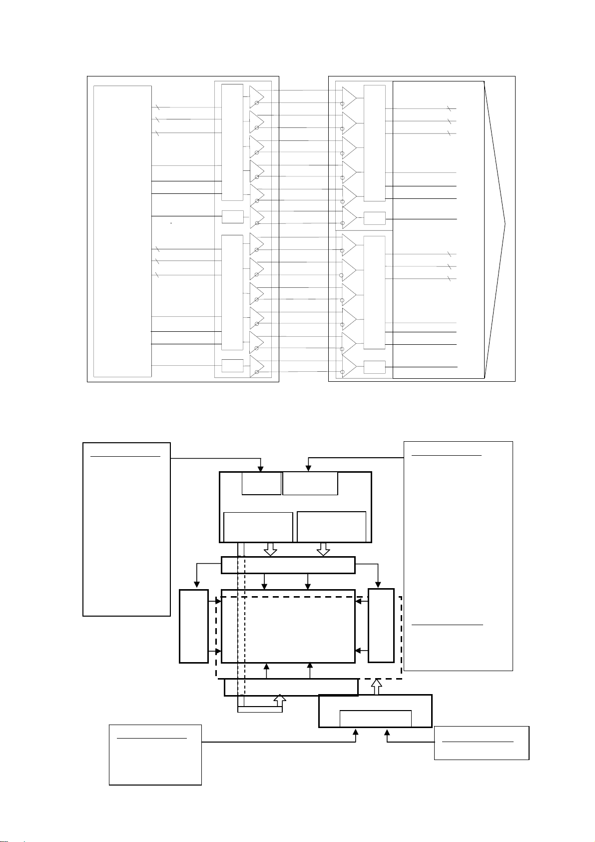
4.2. Interface block diagram
CN1 side:
Contr oller
AR0 AR 9
∼
AG0 AG9
∼
AB0 AB9
∼
ENAB_A
Hsync _A
Vsync _A
CLKA
BR0 ∼ BR9
BG0 ∼ BG9
BB0 ∼ BB9
ENAB_B
Hsync _B
Vsync _B
CLKB
(TV Side)
Port A
10
10
10
LVDS
↑
TTL
PLL
Port B
10
10
10
LVDS
↑
TTL
PLL
2.0KΩ
AIN0+( 13)
AIN0– (12)
AIN1+( 15)
AIN1– (14)
AIN2+( 17)
AIN2– (16)
AIN3+( 23)
AIN3– (22)
AIN4+( 25)
AIN4– (24)
ACK+(20)
ACK– (19)
BIN0+(29)
BIN0– (28)
BIN1+(31)
BIN1– (30)
BIN2+(33)
BIN2– (32)
BIN3+(39)
BIN3– (38)
BIN4+(41)
BIN4– (40)
BCK+(36)
BCK–(35)
3.3
LD- 19Z08-6
(TFT-LCD side)
TTL
↑
LVDS
PLL
TTL
↑
LVDS
PLL
Port A
Port B
10
AR0 AR9
10
AG0
10
AB0 AB9
10
BR0 BR9
10
BG0 BG9
10
BB0 BB9
∼
∼
∼
DE_A
Hsync _A
Vsync _A
CLKA
∼
∼
∼
DE_B
Hsync _B
Vsync _B
CLKB
AG9
LCD Internal Circuit
Corresponding Transmitter: THC63LVD1023 (THine) or equivalent device.
Page 9
CN2 side:
g
Controller
CR0 CR9
∼
CG0 CG9
∼
CB0 CB9
∼
ENAB_C
Hsync _C
Vsync _C
CLKC
DR0 ∼ DR9
DG0 ∼ DG9
DB0 ∼ DB9
ENAB_D
Hsync_ D
Vsync _D
CLKD
LD- 19Z08-7
(TV Side)
Port C
10
10
10
Port D
10
10
10
LVD S
↑
TTL
PLL
LVDS
↑
TTL
PLL
CIN0+(11)
CIN0– (10)
CIN1+(13)
CIN1– (12)
CIN2+(15)
CIN2– (14)
CIN3+(21)
CIN3– (20)
CIN4+(23)
CIN4– (22)
CCK+(18)
CCK– (17)
DIN0+(27)
DIN0– (26)
DIN1+(29)
DIN1– (28)
DIN2+(31)
DIN2– (30)
DIN3+(37)
DIN3– (36)
DIN4+(39)
DIN4– (38)
DCK+(3 4)
DCK–(3 3)
TTL
LVDS
PLL
TTL
LVD S
PLL
(TFT-LCD side)
Port C
↑
Port D
↑
10
CR0 CR9
10
CG0
10
CB0 CB9
DE_C
Hsync _C
Vsync _C
10
DR0 DR9
10
DG0 DG9
10
DB0 DB9
DE_D
Hsync _D
Vsync _D
CLKC
CLKD
∼
∼
CG9
∼
LCD Internal Circuit
∼
∼
∼
Corresponding Transmitter: THC63LVD1023 (THine) or equivalent device.
4.3. Block diagram(LCD Module)
INPUT SIGNALS
CIN0- CIN0+
CIN1- CIN1+
CIN2- CIN2+
CIN3- CIN3+
CIN4- CIN4+
CCK- CCK+
DIN0- DIN0+
DIN1- DIN1+
DIN2- DIN2+
DIN3- DIN3+
DIN4- DIN4+
DCK- DCK+
GATE DRIVER
INPUT SIGNALS
Von,
V
,
BRT
BRT _sel
V
CN2
CONTROL PWB
Control
nals
Si
SOURCE DRIVER
LCD PANEL
1920×3(RGB)×1080
SOURCE DRIVER
CN1
Power Supply
Circuit
GATE DRIVER
INVERTER
CN103, 104
INPUT SIGNALS
Frame
O/S_set
SELLVDS
AIN0- AIN0+
AIN1- AIN1+
AIN2- AIN2+
AIN3- AIN3+
AIN4- AIN4+
ACK- ACK+
BIN0- BIN0+
BIN1- BIN1+
BIN2- BIN2+
BIN3- BIN3+
BIN4- BIN4+
BCK- BCK+
POWER SUPPLY
+12V DC
BACK LIGHT(CCFT×24)
POWER SUPPLY
+24V DC
Page 10
LD- 19Z08-8
4.4. Backlight driving
CN103 (+24V DC power supply and inverter control)
Using connector: S14B-PH-K-S (LF) (JST)
Mating connector: PHR-14 (JST)
Pin No. Symbol Function Default(OPEN) Input Impedance Remark
1 VINV +24V -
2 VINV +24V -
3 VINV +24V -
4 VINV +24V -
5 VINV +24V -
6 GND -
7 GND -
8 GND -
9 GND -
10 GND -
11 Reserved For LCD module internal
usage, should be open
12 VON Inverter ON/OFF GND : pull down
Inverter OFF
13 VBRT Brightness Control 3.3V : pull up
Brightness 100%
14 VBRT_sel Brightness Control
selection
*GND of an inverter board is not connected to GND of a module chassis and a liquid crystal panel drive part.
CN104(+24V DC power supply)
Using connector: S14B-PH-K-S(LF) (JST)
Mating connector: PHR-14 (JST)
Pin No. Symbol Function Default(OPEN) Input Impedance Remark
1 VINV +24V -
2 VINV +24V -
3 VINV +24V -
4 VINV +24V -
5 VINV +24V -
6 GND -
7 GND -
8 GND -
9 GND -
10 GND -
11 Reserved For LCD module internal
usage, should be open
12 Reserved For LCD module internal
usage, should be open
13 Reserved For LCD module internal
usage, should be open
14 Reserved For LCD module internal
usage, should be open
[Note 1] Inverter ON/OFF
Input voltage Function
0V Inverter : OFF
3.3V Inverter : ON
3.3V : pull up
Selected Analog PWM
22K ohm [Note 1]
100K ohm [Note 3]
100K ohm [Note 2]
-
-
Page 11
[Note 2] Brightness Control selection
Pin No.14 is used for the selection of dimming control for V
Input voltage V
BRT
BRT pin (Pin No.13).
0V Pulse dimming
3.3V Analog dimming
[Note 3]Brightness Control
1. Analog Dimming
Brightness control is regulated by analog input voltage (0V to 3.3V).
Input voltage [V
BRT
[Reference]
Brightness ratio[%]
]
MIN TYP MAX Function
0V <-> 3.3V
0V: Dark - 3.3V: Bright
20 <-> 100
[Note] PWM frequency : 275±10Hz
[Note]There is a case that lamp mura may happen, depending on ambient temperature and dimming.
Dimming level should be set according to your evaluation of actual display performance.
(Minimum input voltage 1.5V at below 15℃)
2.Pulse Dimming
Pin No.13 is used for the control of the PWM duty with input pulse from 150Hz to 350Hz.
LD- 19Z08-9
Ta=25℃
Input PWM waveform
High voltage
Low voltage
Ton
ON ON OFF
T
Duty=TON/T
Pulse signal [Hz]
MIN TYP MAX
150 275 350
DUTY(TON/T) [%] 35 <-> 100
Dimming level
[%] 20 <-> 100
(Brightness ratio)
Pulse signal=275Hz
Remark
Ta=25℃
Ta=25℃
[Note]There is a case that lamp mura may happen, depending on ambient temperature,
in dimming. Minimum dimming level should be set according to your evaluation of
actual display performance. (Minimum duty 60% at below 15℃)
[Note]In case of using Pulse Dimming, be careful so that the V
signal (Pin 13) doesn’t have glitch.
BRT
Page 12
LD- 19Z08-10
4.5. The back light system characteristics
The back light system is direct type with 24 CCFTs (Cold Cathode Fluorescent Tube).
The characteristics of the lamp are shown in the following table. The value mentioned below is at the case of one
CCFT.
Item Symbol Min. Typ. Max. Unit Remarks
Life time TL - 60000 - Hour [Note]
[Note]
• Lamp life time is defined as the time when brightness becomes 50% of the original value in the continuous
operation under the condition of Ta=25°C and brightness control(V
=100%).
BRT
• Above value is applicable when the long side of LCD module is placed horizontally (Landscape position).
(Lamp lifetime may vary if LCD module is in portrait position due to the change of mercury density inside
the lamp.)
5. Absolute Maximum Ratings
Parameter Symbol Condition Ratings Unit Remark
Input voltage
(for Control)
12V supply voltage
(for Control)
Input voltage
(for Inverter)
24V supply voltage
(for Inverter)
I
V
VCC
V
ON
V
BRT
VBRT _sel
V
INV
Ta=25 °C
Ta=25 °C
Ta=25 °C
Ta=25 °C
-0.3 ~ 3.6 V [Note 1]
0 ~ + 14 V
0 ~ + 6 V
0 ~ +29 V
Storage temperature Tstg - -25 ~ +60
Operation temperature
(Ambient)
Topa - 0 ~ +50
[Note 1] SELLVDS, FRAME, O/S_set,
[Note 2] Humidity 95%RH Max.(Ta≦40°C)
Maximum wet-bulb temperature at 39 °C or less.(Ta>40°C)
No condensation.
°C
[Note 2]
°C
Page 13

LD- 19Z08-11
6. Electrical Characteristics
6.1. Control circuit driving Ta=25 °C
Parameter Symbol Min. Typ. Max. Uniit Remark
Supply voltage Vcc 11.4 12 12.6 V [Note 1]
+12V supply
voltage
Permissible input ripple voltage VRP - - 100 mVP-P Vcc = +12.0V
threshold voltage
Input leak current (Low)
Input leak current (High)
[Note]VCM: Common mode voltage of LVDS driver.
[Note 1]
Input voltage sequences Dip conditions for supply voltage
0 < t1 ≦ 20ms a) 6.5V ≦ Vcc < 10.8V
10 < t2 ≦ 20ms td ≦ 10ms
10 < t3 ≦ 50ms b) Vcc < 6.5V
0 < t4 ≦ 1s Dip conditions for supply voltage is
t5 ≧ 200ms based on input voltage sequence.
t6 ≧ 0
t7 ≧ 300ms
Current dissipation Icc - 1.1 3.0 A [Note 2]
I
- 13 - A
Inrush current
High VTH - - 100 mV Differential input
Low V
RUSH
- 100 - us
T
RUSH
TL -100 - - mV
V
Input Low voltage VIL 0 - 1.0 V
Input High voltage VIH 2.3 - 3.3 V
IIL1 - - 400 µA
IL2 - - 40 µA
I
IIH1 - - 40 µA
I
IH2 - - 400 µA
Terminal resistor RT - 100 -
Ω
[Note 7]
CM = +1.2V
[Note 6]
[Note 3]
I = 0V
V
[Note 4]
I = 0V
V
[Note 5]
I = 3.3V
V
[Note 4]
I = 3.3V
V
[Note 5]
Differential
input
0.9VCC
0.1Vcc
Vcc
Data1
Data2
Back light:V
t1
t2
ON
t3
INV
t5
OFF
t6
t4
t3
0.9Vcc
0.1Vcc
OFF
Vcc
0.1Vcc
t7
td
V1
V2
※ Data1: ACK±, AIN0±, AIN1±, AIN2±, AIN3±, AIN4±,BCK±, BIN0±, BIN1±, BIN2±, BIN3±, BIN4±
*V
voltage pursues the sequence mentioned above
CM
※ Data2: SELLVDS, FRAME, O/S_SET
V1:10.8V
V2:6.5V
Page 14

LD- 19Z08-12
[Note]About the relation between data input and back light lighting, please base on the above-mentioned input
sequence. When back light is switched on before panel operation or after a panel operation stop, it may not
display normally. But this phenomenon is not based on change of an incoming signal, and does not give
damage to a liquid crystal display.
[Note 2] Typical current situation: 1024 gray-bar patterns. (Vcc = +12.0V)
The explanation of RGB gray scale is seen in section 8.
RGB
GS0
RGB
GS1
RGB
GS2
....
RGB
GS1022
RGB
GS1023
Vcc=+12.0V
CK=74.25MHz
Th=7.41μs
[Note 3] SELLVDS, FRAME, O/S_SET
[Note 4] O/S_SET
[Note 5] FRAME, SELLVDS
[Note 6] ACK±, AIN0±, AIN1±, AIN2±, AIN3±, AIN4±,BCK±, BIN0±, BIN1±, BIN2±, BIN3±, BIN4±
[Note 7] Vcc12V inrush current waveform
t1 = 50us
Vcc
Irush = 13A
Icc
Trush = 100us
Page 15

V
V
V
V
6.2. Inverter driving for back light
The back light system is
direct type with 24 CCFTs (Cold Cathode Fluorescent Tube).
Parameter Symbol Min. Typ. Max. Unit Remark
LD- 19Z08-13
Current dissipation 1 IINV 1 - 11.8 13.0 A
+24V
Current dissipation 2 IINV 2 - 10.3 11.5 A
Supply voltage VINV 22.8 24.0 25.2 V
Permissible input ripple voltage VRF - - 300 mV
Input voltage (Low) V
Input voltage (High) V
0 - 1.0 V
ONL
2.3 - 3.6 V
ONH
[Note 1] 1) VINV-turn-on condition
INV
ON,VBRT
INV-turn-off condition
2) V
, V
ON
BRT
1.0V
21.6V
0V
T1
T2
2.0V
p-p
T1>100μs
≧1ms
T2
t1≧1ms
VINV = 24V, Ta=25°C
= 3.3V
V
BRT
[Note 1,2]
VINV = +24.0V
V
ON,VBRT
VBRT _sel
,
t1
INV
1.0V
0V
21.6V
0V
[Note 2] Current dissipation 1 : Definition within 60 minutes after turn on. (Rush current is excluded.)
Current dissipation 2 : Definition more than 60minutes after turn on.
Page 16

7. Timing characteristics of input signals
7.1. Timing characteristics
Timing diagrams of input signal are shown in Fig.2.
Parameter Symbol Min. Typ. Max. Unit Remark
Clock Frequency 1/Tc 55 74.25
Horizontal period TH
Data enable
signal
[Note]-When vertical period is very long, flicker and etc. may occur.
-Please turn off the module after it shows the black screen.
-As for your final setting of driving timing, we will conduct operation check test at our side, please
inform your final setting.
DE
Aport DATA
(R,G,B)
Bport DATA 2
(R,G,B)
Cport DATA
(R,G,B)
Dport DATA
(R,G,B)
DE
Horizontal period (High) THd
Vertical period TV
Vertical period (High) TVd 1080 1080 1080 line
TH
1
3
1920 1920
Tc
4
TV
5
6
7 1919 1919
8
Fig.2 Timing characteristics of input signals
80
515
6.94
480
1120
73.052
THd
1 2 1080
550
7.41
480
1125
120
TVd
825
11.1
480
1232
120.54
1917 1917
1918 1918
1079
LD- 19Z08-14
MHz
clock
µs
clock
line
Hz
Page 17

7.2. Input data signal and display position on the screen
R1 G1 B1 R2 G2 B2
(1、1) (1,2)
R1 G1 B1 R2 G2 B2
(1、3) (1,4)
LD- 19Z08-15
1・1 1・2 1・3
2・1 2・2
3・1
1080・1
1・4
R G B
Display position of Dat (V,H)
1・1920
1080・1920
Page 18

LD- 19Z08-16
8. Input Signal, Basic Display Colors and Gray Scale of Each Color
Colors &
Gray scale
Black – 0 0 0 0 0 0 0 0 0 0 0 0 0 0 0 0 0 0 0 0 0 0 0 0 0 0 0 0 0 0
Blue – 0 0 0 0 0 0 0 0 0 0 0 0 0 0 0 0 0 0 0 0 1 1 1 1 1 1 1 1 1 1
Green – 0 0 0 0 0 0 0 0 0 0 1 1 1 1 1 1 1 1 1 1 0 0 0 0 0 0 0 0 0 0
Cyan – 0 0 0 0 0 0 0 0 0 0 1 1 1 1 1 1 1 1 1 1 1 1 1 1 1 1 1 1 1 1
Red – 1 1 1 1 1 1 1 1 1 1 0 0 0 0 0 0 0 0 0 0 0 0 0 0 0 0 0 0 0 0
Basic Color
Magenta – 1 1 1 1 1 1 1 1 1 1 0 0 0 0 0 0 0 0 0 0 1 1 1 1 1 1 1 1 1 1
Yellow – 1 1 1 1 1 1 1 1 1 1 1 1 1 1 1 1 1 1 1 1 0 0 0 0 0 0 0 0 0 0
White – 1 1 1 1 1 1 1 1 1 1 1 1 1 1 1 1 1 1 1 1 1 1 1 1 1 1 1 1 1 1
Black GS0 0 0 0 0 0 0 0 0 0 0 0 0 0 0 0 0 0 0 0 0 0 0 0 0 0 0 0 0 0 0
R0 R1 R2 R3 R4 R5 R6 R7 R8 R9 G0 G1 G2 G3 G4 G5 G6 G7 G8 G9 B0 B1 B2 B3 B4 B5 B6 B7 B8 B9
Gray
Scale
× GS1 1 0 0 0 0 0 0 0 0 0 0 0 0 0 0 0 0 0 0 0 0 0 0 0 0 0 0 0 0 0
Darker GS2 0 1 0 0 0 0 0 0 0 0 0 0 0 0 0 0 0 0 0 0 0 0 0 0 0 0 0 0 0 0
×
Ø
Brighter GS1021 1 0 1 1 1 1 1 1 1 1 0 0 0 0 0 0 0 0 0 0 0 0 0 0 0 0 0 0 0 0
↓
↓
↓
↓
Gray Scale of Red
Ø GS1022 0 1 1 1 1 1 1 1 1 1 0 0 0 0 0 0 0 0 0 0 0 0 0 0 0 0 0 0 0 0
Red GS1023 1 1 1 1 1 1 1 1 1 1 0 0 0 0 0 0 0 0 0 0 0 0 0 0 0 0 0 0 0 0
Data signal
↓
↓
↓
↓
Black GS0 0 0 0 0 0 0 0 0 0 0 0 0 0 0 0 0 0 0 0 0 0 0 0 0 0 0 0 0 0 0
× GS1 0 0 0 0 0 0 0 0 0 0 1 0 0 0 0 0 0 0 0 0 0 0 0 0 0 0 0 0 0 0
Darker GS2 0 0 0 0 0 0 0 0 0 0 0 1 0 0 0 0 0 0 0 0 0 0 0 0 0 0 0 0 0 0
×
Ø
Brighter GS1021 0 0 0 0 0 0 0 0 0 0 1 0 1 1 1 1 1 1 1 1 0 0 0 0 0 0 0 0 0 0
Gray Scale of Green
Ø GS1022 0 0 0 0 0 0 0 0 0 0 0 1 1 1 1 1 1 1 1 1 0 0 0 0 0 0 0 0 0 0
Green GS1023 0 0 0 0 0 0 0 0 0 0 1 1 1 1 1 1 1 1 1 1 0 0 0 0 0 0 0 0 0 0
Black GS0 0 0 0 0 0 0 0 0 0 0 0 0 0 0 0 0 0 0 0 0 0 0 0 0 0 0 0 0 0 0
↓
↓
↓
↓
↓
↓
↓
↓
× GS1 0 0 0 0 0 0 0 0 0 0 0 0 0 0 0 0 0 0 0 0 1 0 0 0 0 0 0 0 0 0
Darker GS2 0 0 0 0 0 0 0 0 0 0 0 0 0 0 0 0 0 0 0 0 0 1 0 0 0 0 0 0 0 0
Ø
Ø
Brighter GS1021 0 0 0 0 0 0 0 0 0 0 0 0 0 0 0 0 0 0 0 0 1 0 1 1 1 1 1 1 1 1
Gray Scale of Blue
Ø GS1022 0 0 0 0 0 0 0 0 0 0 0 0 0 0 0 0 0 0 0 0 0 1 1 1 1 1 1 1 1 1
Blue GS1023 0 0 0 0 0 0 0 0 0 0 0 0 0 0 0 0 0 0 0 0 1 1 1 1 1 1 1 1 1 1
↓
↓
↓
↓
↓
↓
↓
↓
0: Low level voltage, 1: High level voltage.
Each basic color can be displayed in 1024 gray scales from 10 bits data signals. According to the combination of
total 30 bits data signals,
one billion
-color display can be achieved on the screen.
Page 19

9. Optical characteristics
Ta=25°C, Vcc=12.0V, VINV =24.0V, V
Parameter Symbol Condition Min. Typ. Max. Unit Remark
θ
Viewing angle
range
Horizontal
Vertical
θ
θ
θ
21
22
11
12
CR≧10
70 88 - Deg.
70 88 -
Contrast ratio CRn 1200 1800 - [Note2,4]
τ
Response time
White
Red
Chromaticity
Green
Blue
r
τ
d
- 4 - ms [Note3,4,5]
x 0.242 0.272 0.302 y 0.247 0.277 0.307 x 0.610 0.640 0.670 y 0.300 0.330 0.360 -
θ
=0 deg.
x 0.250 0.280 0.310 y 0.570 0.600 0.630 x 0.120 0.150 0.180 y 0.030 0.060 0.090 -
Luminance White YL 360 450 - cd/m2
BRT
LD- 19Z08-17
=100%,Timing:60Hz(typ. value)
[Note1,4]
Deg.
[Note4]
Luminance
uniformity
White
Measurement condition: Set the value of V
δw
to maximum luminance of white.
BRT
- - 1.25 - [Note 6]
*The measurement shall be executed 60 minutes after lighting at rating.
[Note]The optical characteristics are measured using the following equipment.
Detector(EZ-CONTRAST/ Photodiode)
400mm
Middle of the screen (θ=0°)
Middle of the screen (θ=0°)
TFT-LCD Module
TFT-LCD Module
Fig.4-1 Measurement of viewing angle range and
Response time.
Viewing angle range: EZ-CONTRAST
Response time: Photodiode
Fig.4-2 Measurement of Contrast, Luminance,
Chromaticity.
Detector(SR-3)
Field=1°
Page 20

LD- 19Z08-18
[Note 1]Definitions of viewing angle range
Normal line
θ
11
θ
21
θ
12
θ
22
6 o’clock direction
[Note 2]Definition of contrast ratio :
The contrast ratio is defined as the following.
Luminance (brightness) with all pixels white
Contrast Ratio
=
Luminance (brightness) with all pixels black
[Note 3]Definition of response time
The response time (τ
and τr) is defined as the following figure and shall be measured by switching the input
d
signal for “any level of gray (0%, 25%, 50%, 75% and 100%)” and “any level of gray (0%, 25%, 50%, 75%
and 100%)”.
0%
0%
25%
50%
75%
100%
td: 25%-0%
td: 50%-0% td: 50%-25%
td: 75%-0% td: 75%-25% td: 75%-50%
td: 100%-0% td: 100%-25% td: 100%-50% td:100%-75%
25% 50% 75%
tr:0%-25%
tr:0%-50% tr:0%-75% tr:0%-100%
tr: 25%-50% tr25%-75% tr: 25%-100%
tr: 50%-75% tr: 50%-100%
100%
tr: 75%-100%
t*:x-y...response time from level of gray(x) to level of gray(y)
τ
= Σ(tr:x-y)/10 , τd = Σ(td:x-y)/10
r
Bright
100%
90%
Dark
Bright
Photodetector
10%
Output
0%
τd τr
time
[Note 4]This shall be measured at center of the screen.
[Note 5] This value is valid when O/S driving is used at typical input time value.
Page 21

LD- 19Z08-19
[Note 6]Definition of white uniformity ;
White uniformity is defined as the following with five measurements. (A∼E)
Maximum luminance of five points (brightness)
W=
δ
Minimum luminance of five points (brightness)
480
960 1440
A
C
B
pixel
D
E
10. Handling Precautions of the module
a) Be sure to turn off the power supply when inserting or disconnecting the cable.
b) This product is using the parts (inverter, CCFT etc), which generate the high voltage.
Therefore, during operating, please don't touch these parts.
c) Brightness control voltage is switched for “ON” and “OFF”, as shown in Fig.4. Voltage difference generated
by this switching, ΔV
inverter and its surrounding circuit. So, separate the power supply of the inverter circuit with the one of its
surrounding circuit.
INV, may affect a sound output, etc. when the power supply is shared between the
270
540
810
pixel
ΔVINV
VINV
IINV
PWM control
signal
0V
0A
ON ON OFF
0V
Fig.4 Brightness control voltage.
*Since inverter board’s GND is not connected to the frame of the LCD module, please connect it with the
Customer’s GND of inverter power supply.
d) Be sure to design the cabinet so that the module can be installed without any extra stress such as warp or
twist.
e) Since the front polarizer is easily damaged, pay attention not to scratch it.
f) Since long contact with water may cause discoloration or spots, wipe off water drop immediately.
g) When the panel surface is soiled, wipe it with absorbent cotton or other soft cloth.
h) Since the panel is made of glass, it may break or crack if dropped or bumped on hard surface. Handle with
care.
Page 22

LD- 19Z08-20
i) Since CMOS LSI is used in this module, take care of static electricity and take the human earth into
consideration when handling.
j) The module has some printed circuit boards (PCBs) on the back side, take care to keep them form any stress
or pressure when handling or installing the module; otherwise some of electronic parts on the PCBs may be
damaged.
k) Observe all other precautionary requirements in handling components.
l) When some pressure is added onto the module from rear side constantly, it causes display non-uniformity
issue, functional defect, etc. So, please avoid such design.
m) When giving a touch to the panel at power on supply, it may cause some kinds of degradation. In that case,
once turn off the power supply, and turn on after several seconds again, and that is disappear.
n) When handling LCD modules and assembling them into cabinets, please be noted that long-term storage in
the environment of oxidization or deoxidization gas and the use of such materials as reagent, solvent,
adhesive, resin, etc. which generate these gasses, may cause corrosion and discoloration of the LCD
modules.
o) This LCD module is designed to prevent dust from entering into it. However, there would be a possibility to
have a bad effect on display performance in case of having dust inside of LCD module. Therefore,
please ensure to design your TV set to keep dust away around LCD module.
11. Packing form
a) Piling number of cartons:2 maximum
b) Packing quantity in one carton:8pcs
c) Carton size:1320(W) × 1110(D) × 940(H)
d) Total mass of one carton filled with full modules:225kg(Max)
12. Reliability test item
No. Test item Condition
1
2
3
4
5
6
7
8
[Result evaluation criteria]
Under the display quality test condition with normal operation state, there shall be no change, which may
affect practical display function.
High temperature storage test
Low temperature storage test
High temperature and high humidity
operation test
High temperature operation test
Low temperature operation test
Vibration test
(non-operation)
Shock test
(non-operation)
ESD
Ta=60°C 240h
Ta=-25°C 240h
Ta=40°C ; 95%RH 240h
(No condensation)
Ta=50°C 240h
Ta=0°C 240h
Frequency: 10~57Hz/Vibration width (one side): 0.075mm
: 58~500Hz/Acceleration: 9.8 m/s²
Sweep time: 11 minutes
Test period: 3 hours (1h for each direction of X, Y, Z)
Maximum acceleration: 294m/s
Pulse width: 11ms, sinusoidal half wave
Direction: +/-X, +/-Y, +/-Z, once for each direction.
* At the following conditions, it is a thing without incorrect
operation and destruction.
(1)Non-operation: Contact electric discharge ±10kV
Non-contact electric discharge ±20kV
(2)Operation Contact electric discharge ±8kV
Non-contact electric discharge ±15kV
Conditions: 150pF, 330ohm
2
Page 23

LD- 19Z08-21
(
)
(
)
13. Others
1) Lot No. Label ;
The label that displays SHARP, product model (LK520D3LZ97), a product number is stuck on the back of the
module.
【LK520D3LZ97X,T】NSEC PRODUCTION
【LK520D3LZ97Z,V】SEMEX PRODUCTION
2) Packing Labe
【LK520D3LZ97X,T】 【LK520D3LZ97Z,V】
社内品番:
Bar code
LotNO.
Bar code
Quantity:
Bar code
ユーザ品番
シャープ物流用ラベルです。
LK520D3LZ97
7Z S00001 X(orT)
LK520D3LZ97
7Z S00001 Z(orV)
A production year(the last figures of the Christian Era)
4S
LK520D3LZ97X(orT)(①)
(1T)2007. *.** (②)
(Q)
8
① Management No.
② Lot No. (Date)
③ Quantity
3) Adjusting volume has been set optimally before shipment, so do not change any adjusted value.
If adjusted value is changed, the specification may not be satisfied.
4) Disassembling the module can cause permanent damage and should be strictly avoided.
Module No.
Barcode
Lot No.
Module No.
Barcode
Lot No.
A production month (1-9, X,Y, Z)
社内品番:
Bar code
LotNO.
Bar code
pcs (③)
Quantity:
Bar code
ユーザ品番
シャープ物流用ラベルです。
How to express Lot No.
○
○ ○ ○ ○ ○ ○ ○
Serial No.
Management No.
4S
LK520D3LZ97Z(orV)(①)
(1T)2007. *.** (②)
(Q)
8
pcs (③)
Page 24

LD- 19Z08-22
5) Please be careful since image retention may occur when a fixed pattern is displayed for a long time.
6) The chemical compound, which causes the destruction of ozone layer, is not being used.
7) Cold cathode fluorescent lamp in LCD PANEL contains a small amount of mercury. Please follow local
ordinances or regulations for disposal. This sentence is displayed on the backside of the module.
9) Rust on the module is not taken up a problem.
10) C-PWB must be on upper side of LCD module when it is in the TV-set.
*:Please inform SHARP if C-PWB is at bottom side of LCD module when it is in the TV-set
11) This module is corresponded to RoHS.
14. Carton storage condition
Temperature 0°C to 40°C
Humidity 95%RH or less
Reference condition : 20°C to 35°C, 85%RH or less (summer)
: 5°C to 15°C, 85%RH or less (winter)
• the total storage time (40°C,95%RH) : 240H or less
Sunlight Be sure to shelter a product from the direct sunlight.
Atmosphere Harmful gas, such as acid and alkali which bites electronic components and/or
wires must not be detected.
Notes Be sure to put cartons on palette or base, don’t put it on floor, and store them with
removing from wall
Please take care of ventilation in storehouse and around cartons, and control
changing temperature is within limits of natural environment
Storage life 1 year
Page 25

LD-19Z08-23
Page 26

Page 27

Page 28

TO :
File No.
ISSUE
PAGE
LDK-145E
19-Dec-07
10page
Incoming Inspection Standards
Product
Model
□CUSTOMER'S APPROVAL
DATE
BY BY
TFT-LCD Module
LK520D3LZ97
PRESENTED
LDK-145E-1
K.Sogame
DEPARTMENT GENERAL MANAGER
QUALITY ASSURANCE DEPT.
AVC LIQUID CRYSTAL DISPLAY GROUP
SHARP CORPORATION
Page 29

Records of Revision
Standards
No.
LDK-145E 19-Dec-07
Revision
Date
Rev.
Mark
- first Edition Model Addition : LK520D3LZ97
Contents of Revision
LDK-145E-2
Page 30

Applicable Model List
This grade inspection standard applies to the models as below
Applicable Model
LK520D3LZ97
Revision
Mark
LDK-145E-3
Page 31

Incoming Inspection for TFT-LCD Module
1. Scope
- These Incoming Inspection Standards shall apply to TFT-LCD Modules supplied by AVC LCD Group.
Sharp Corporation to LG Electronics INC
2. Inspection Lot
- Quantity per shipment lot is ONE Inspection lot.
3. Incoming Inspection Condition
3.1 Condition of Lot Judgement
- Unless otherwise agreed in writing, the method of incoming inspection shall be in accordance with
a sampling inspection based on ISO 2859-1
- Sampling Table : Table in ISO 2859-1
- Sampling Type : Single Sampling Plan
- Inspection Level : Level Ⅱ, Normal Inspection
- Acceptable quality level (AQL) : Major defects: AQL: 0.4
: Minor defects: AQL: 1.0
- Defects are classified as major defect and minor defect according to Classification on Defects Minor & Majors of item# 6.
a) Major defect: Major defect is a defect that is likely to result in failure, or to reduce materially
the usability of the product for its intended purpose.
b) Minor defect: Minor defect is a defect that is assumed to be little or no obstacle to usability of inspection unit,
effective usage ro operation of the product.
3.2 Operational Inspection Condition
- The inspection shall be conducted in the standard operative condition described in the specification.
- The external illumination on the Module: 300 ~ 700lx (Standard 500lx)
- The viewing distance between center of panel surface on the Module and the eyes of the inspector.
*Refer to Fig.1 and Fig.2 [Inspection :Viewing Angle from Left to Right ± 45 degrees]
[1] Apply to Foreign material, Bright Dot and Black Dot.
[2] Apply to defect concerned with Mura (Display Uniformity)
- Backlight Luminance: Based on value which is desuribed in the specificatio.(Brightness Control : 100%)
- Ambient temperature: 24℃ ± 2℃ in principle
- Ambient humidity: 65 ± 5% RH in principle
Fig.1) Judgment position of Operational Inspection Inspector
Viewing Angle
the inspector shall be within ± 45 degrees from
Left to Right
LCD Module
[1]750±50mm
[2]2,000± 500 mm
: The surface of the Module and the eyes of
Eyes
Illuminance Meter
( 300 ~ 700 lx on this condition)
LDK-145E-4
Page 32

Fig.2) How to use ND Filter
r
r
[1] Apply to Bright Dot and Tiny Bright Dot (Small dots seem to be bright by foreign material)
ND filter is moved to the panel side closer and judged.
ND Filte
LCD Module
750 ± 50 mm
[2] Apply to defect concerned with Mura (Display Uniformity)
ND filter is moved to the eyes closer and judged.
ND Filte
LCD Module
2,000 ± 500 mm
3.3 Appearance Inspection Condition
*1: In the operational inspection condition, the distance between the Module and eyes of the inspector shall be
750mm or MORE. (Condition of lighting B/L and operating Module on White picture)
*2: In the operational inspection condition, the distance between the Module and eyes of the inspector shall be
750mm or MORE. (Condition of lighting B/L and operating Module on Black picture)
*3: The external illuminance of panel surface; 900-1500lx (Standard: 1200lx)
Shall be conducted with fluorescent lamp lighting on working bench. [Refer to Fig.3]
The visual observation shall be conducted with the judgement distance that is 350±100mm between the panel and
the inspector's eyes. (Condition of Non-operating)
Fig.3) Judgement position of Appearance Inspecion Inspector
Fluorescent Lamp
[Note] Applicable range of Appearance inspection is
out side by 3.0 mm from the effective display area.
Eyes
[Note] Scratch/Dent on the rear polarizer is not counted,
Illuminance Meter
(900 ~ 1500lx on this condition)
if it is not found from the front side by B/L lighting
condition.
350±100mm
LCD Module
LDK-145E-5
Page 33

4. Standards for Display Quality Inspection
4.1 Zone
L
H
4.2 Definition
a) Bright dot
Full-time lighting dot in the black display.
- Visible through 5% ND filter : Counted as Bright dot
- Not visible through 5% ND filter : Non count
b) Tiny bright dot
Small dots seem to be bright by foreign material
- Visible through 5% ND filter : Tiny bright dots(Counted as Bright dot)
- Not visible through 5% ND filter : Bright foreign material
c) Black dot
Dot which seems to come out in black on the white display and Red/Green/Blue monochromatic display.
There are full-dot black dot and half-dot one due to the multi-pixel structure.
・H and L are assumed all the effective display area.
Fig.4) Example: Full black dot & Half black dot
Half black dotFull black dot
d) Scratches on color filter
*White dot on the Black display.
- Visible through 5% ND filter : Tiny bright dots(Counted as Bright dot)
- Not visible through 5% ND filter : Bright foreign material
e) Scratches on black mask
*White dot around R/G/B dot (black mask part) on the black display.
- Visible through 5% ND filter : Tiny bright dots(Counted as Bright dot)
- Not visible through 5% ND filter : Bright foreign material
[Target Area]
Target area is from active area to 1.5mm (High density is NG)
Fig.5) Example: Scratch on the
color filter
Fig.6) Example: Scratch on the
black mask
f) Line defect (Vertical / Horizontal / Cross)
*All kinds of line defects such as Vertical, Horizontal or Cross are not allowed.
g) Display Mura (Non-Uniformity)
* Non-Uniformity of display brightness.
LDK-145E-6
Page 34

4.3 Bright dot
Check pattern
Black pattern
(Refer to Item# 4.2)
Acceptable total number of Bright dot
0
4.4 Black dot
Check pattern
Acceptable total number of Black dot
Full Black dot(B)Half Black dot(A)
Joined Black dots(C)
Total=1/2×(A)+(B)+2×(C)
White pattern and at each
pattern of R, G and B
816
4
8
(Refer to Item#4.2)
[ Note ] Flashing dot is counted as a Black dot
[ Note ] Joined Black dots shall be based on “Explanation for Black Dot criterion and Judgement method.”
[ Note ] Joined more than 1.5 Black dots by Vertical shall be judged NG.
4.5 Distance of Black Dot
- Full Black dot,Joined Black dots - Full Black dot,Joined Black dots : Acceptable if it is more than 15mm
- Half Black dot - Half Black dot : Acceptable if it is Max 3 dots within 5mm φ
- Full Black dot,Joined Black dots - Half Black dot : Acceptable if it is more than 15mm
5. Appearance Inspection Criterion
[ Permissible Nnumber: N, Average Diameter(Fig.7): D (mm), Length(Fig.8): L (mm) ]
Item
Foreign material
(in the polarizer /
backlight / cell)
Bright Foreign material
(in the polarizer / cell)
Circular
Linear
Judgment Criterion
0.3≦D≦0.8 , N≦10
L≦3.0 , N≦3
0.1≦D≦0.5 , N≦10
Not visible through 5% ND filter.
Appearance Inspection
Condition
Condition of operation
(Refer to *1 of Item#3.3)
Condition of operation
(Refer to *1 & *2 of Item#3.3)
Condition of operation
(Refer to *2 of Item#3.3)
Scratches on the polarizer/glass
Dents on the polarizer/glass
Fig.7) Average diameter : D
a+b
D =
a
b
L≦10.0 , N≦4
0.3≦D≦0.8 , N≦10
0.3>D:No count
LDK-145E-7
Condition of Non operation
(Refer to *3 of Item#3.3)
Fig.8) Length : L
L = The longest position
L
Page 35

6. Classification on Defects Minor & Majors
Classifica
tion
Inspection item Criterion for defects / Judgment
A power supply voltage shall be a standard value described in the specification.
Defect type
Operating frequency
Current consumption
Contrast ratio
(1) Does not meet the specified range in the specification
(2) Does not meet the specified range in the specification
(3) Does not meet the specified range in the specification
(4)
(5) Vertical line defect
Display Inspection
(6) Horizontal line defect
Characteristic of electricity and mechanical
Scratches and dent
on the polarizer
(7) Cross line defect
(8) Shall be accordance with the Item#
"5.Appearance Inspection Criterion"
(9) Shall be accordance with the Item#
Bubble in the polarizer
"5.Appearance Inspection Criterion"
(10) Shall be accordance with the Item#
Foreign material
"5.Appearance Inspection Criterion"
Appearance of Bezel
(11) Irregular plating / lrregular Coating / Rust on the edge are ignored
(12) a)The lead wire is broken.
Major
Major
Major
MajorCorrect pattern is not displayed when the display pattern is input.
Major
Major
Major
Minor
Minor
Minor
Minor
Major
Criterion for External Quality
Damaged Material
Bright dot
Scratch on the color filter
Scratch on the black mask
Black dot
Display Mura
(Non-uniformity)
Criterion for Display Quality
Remained electric
charge
b)Although the lead wire is not broken (not disconnected) and does not
affect the operation and reliability of LCD module it has scratch.
c)Failure is found concerning function or performance,
or product value is impaired in appearance.
(13) Exceed permissible value
(14) Exceed permissible value
(15) Exceed permissible value
(16) Exceed permissible value (Flashing dot is classified as a black dot)
(17) There should not be Non-uniformity through 5%ND filter.
(18) Electric charge is remained for more than 3seconds in the α-zone
immediately after power-off.
(Illuminance condition around : 300~700lx(standard 500lx))
Within 3
[Inspection condition]
seconds
-Signal power is off
α zone
20mm -B/L power is on
Minor
Major
Minor
Minor
Minor
Minor
Minor
Minor
LDK-145E-8
Page 36

Classificat
ion
Inspection item
Defect typeCriterion for defects /determinations
Criterion for Display QualityOthers
PI Repellent
Long time
afterimage
Short time
afterimage
Shadowing
(19) One dot-shaped black stain is considered as “good product”.(But, if it seems to be
bright dot when changing viewing angle, it’ll be counted as small bright dot)
(20)
Afterimage of the former pattern is not disappeared within 10 seconds when a pattern was
displayed for 30 minutes and switch to another pattern.
(21) After display same pattern for 5 seconds, the afterimage is not disappeared within 10 seconds.
(22)
The brightness difference between A section and B section is visible through
10%ND filter.
B
(700, 475)
A
(1220, 605)
Ambient: V64
Window : V255
Minor
Minor
Minor
Minor
Outline
(23) Does not meet specified range in the specification
dimensions
Weight
Rating label
(24) Does not meet specified range in the specification
(25) A) The one that is forgetting, misprinting or not-readable.
(Readable one should be a good one.)
(Sealing/Display
label)
B) As for the display label, peel-off is more than the degree of 1/10 of total area .
(except for legible one among discoloration of display label.)
[Note]Regarding the items to use limit samples, limit samples should have priority over others
7.Others
In case any doubts arise on the items, both Parties shall cooperate in an effort to settle it down.
Major
Major
Major
Minor
LDK-145E-9
Page 37

Explanation for Black Dot criterion and Judgment method
e
t
p
j
Judgment Method
Example
RGB RGB RGB RGB RGB RGB
A half dot not lit on each color
screen of R, G or B is judged
Half Black dot with one defect.
R half black dot
G half black dot
B half black dot
one dfect one defect one defect
A one dot not lit on each color R G B R G B R G B
screen of R, G or B is judged
Full Black dot with one defect.
R full black dot G full black dot
B full black dot
one dfect one defect one defect
Dots seemed continuous R G B R G B R G B R G B R G B R G B R G B R G B R G B
with Horizontal and Slant
on each color screen of
R, G or B is judged
Joined Black dots with
one defect.
Judgment Method
Dots seemed continuous
with Horizontal and Slant
on each color screen of
R, G or B is judged
Full Black dot with one defect.
Example
Full black dot Full black dot Full black dot
one defect one defect one defect
RGB RGB
Full black dot
one defect
Full black dot
defec
on
A black dot within a pixel on
each color screen of R, G or B
(black mode opened one dot)
is counted one defect.
Distance between the black
dots is not judged.
1 pixel = 1 dot each of R+G+B
Dots seemed joined with
Vertical on each color screen
of R, G or B are NG.
Joined 3 dots on each color
screen is judged
of R, G or B are NG.
Joined Black dots
one defect
Joined Black dots
one defect
Joined Black dots
one defect
Full black dot Full black dot Full black dot
one defect one defect one defect
RGBRGB RGBRGB RGB RGB
Joined Black dots
one dfect
Joined Black dots
one dfect
Full black dot Full black dot
one defect one defect
RGB RGB RGB RGBRGB RGBRGB
NG NG NG
Distance between the
black dots exceeding
one pixel on the white
screen is re
ected.
Distance to
be judged
Distance between the
black dots is NG
Circle diameter
of 5mm
Distance to
be judged
Distance between the
black dots is NG
max 3 dots
RGBRGB RGB RGB
NG NG NG
Distance between black dot
"A" to black dot "B" is
15mm or more in a white
icture
More than15mm
A
Black dot [A]
・Full Dot
・Joined Dot
B
Black dot [B]
・Full Dot
・Joined Dot
・Half Dot
Distance between the
black dots is ok
Distance between the
black dots is ok
RGBRGB RGB RGB
Distance between the
black dots is OK
Distance between the
black dots is NG
LDK-145E-10
 Loading...