

Page 1
Global LCD Panel Exchange Center
www.panelook.com
One step solution for LCD / PDP / OLED panel application: Datasheet, inventory and accessory!
www.panelook.com
Page 2
Global LCD Panel Exchange Center
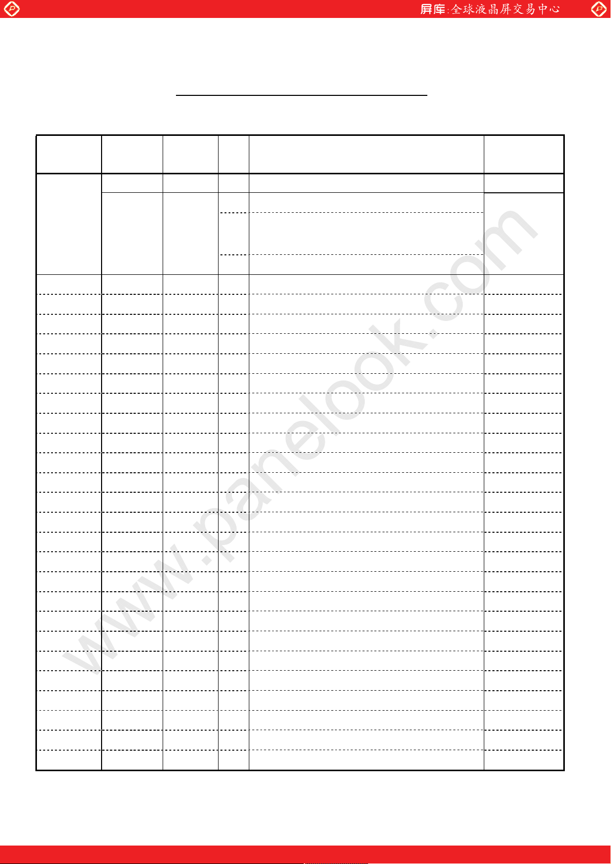
RECORDS OF REVISION
MODEL No. : LK520D3LZ88
SPEC No. : LD-20125A
www.panelook.com
SPEC No. DATE
LD-20125
2008.1.17
2008.2.25
REVISED
A
No.
㧙㧙
PAGE SUMMARY NOTE
2 Changed the Mating LVDS transmitter
20 Changed the Lot No Label
21 Added comment about UL label
㧙
(Identification Code)
1st Issue
2nd Issue
One step solution for LCD / PDP / OLED panel application: Datasheet, inventory and accessory!
www.panelook.com
Page 3
Global LCD Panel Exchange Center
1. Application
This specification applies to the color 52.0” TFT-LCD module LK520D3LZ88.
* These technical literature are proprietary products of SHARP CORPORATION (“SHARP”) and include materials
protected under copyright of SHARP. Do not reproduce or cause any third party to reproduce them in any form or by
any means, electronic or mechanical, for any purpose, in whole or in part, without the express written permission of
SHARP.
* In case of using the device for applications such as control and safety equipment for transportation (aircraft, trains,
automobiles, etc.), rescue and security equipment and various safety related equipment which require higher
reliability and safety, take into consideration that appropriate measures such as fail-safe functions and redundant
system design should be taken.
* Do not use the device for equipment that requires an extreme level of reliability, such as aerospace applications,
telecommunication equipment (trunk lines), nuclear power control equipment and medical or other equipment for
life support.
* SHARP assumes no responsibility for any damage resulting from the use of the device that does not comply with
the instructions and the precautions specified in these specification.
* Contact and consult with a SHARP sales representative for any questions about this device.
2. Overview
This module is a color active matrix LCD module incorporating amorphous silicon TFT (Thin Film Transistor). It is
composed of a color TFT-LCD panel, driver ICs, control circuit, power supply circuit, inverter circuit and back light
system etc. Graphics and texts can be displayed on a 1920RGB1080 dots panel with
using LVDS (L
This module also includes the DC/AC inverter to drive the CCFT. (+24V of DC supply voltage)
And in order to improve the response time of LCD, this module applies the Over Shoot driving (O/S driving)
technology for the control circuit .In the O/S driving technology, signals are being applied to the Liquid Crystal
according to a pre-fixed process as an image signal of the present frame when a difference is found between image
signal of the previous frame and that of the current frame after comparing them.
With this technology, image signals can be set so that liquid crystal response completes within one frame. As a
result, motion blur reduces and clearer display performance can be realized.
ow Voltage Differential Signaling) to interface, +12V of DC supply voltages.
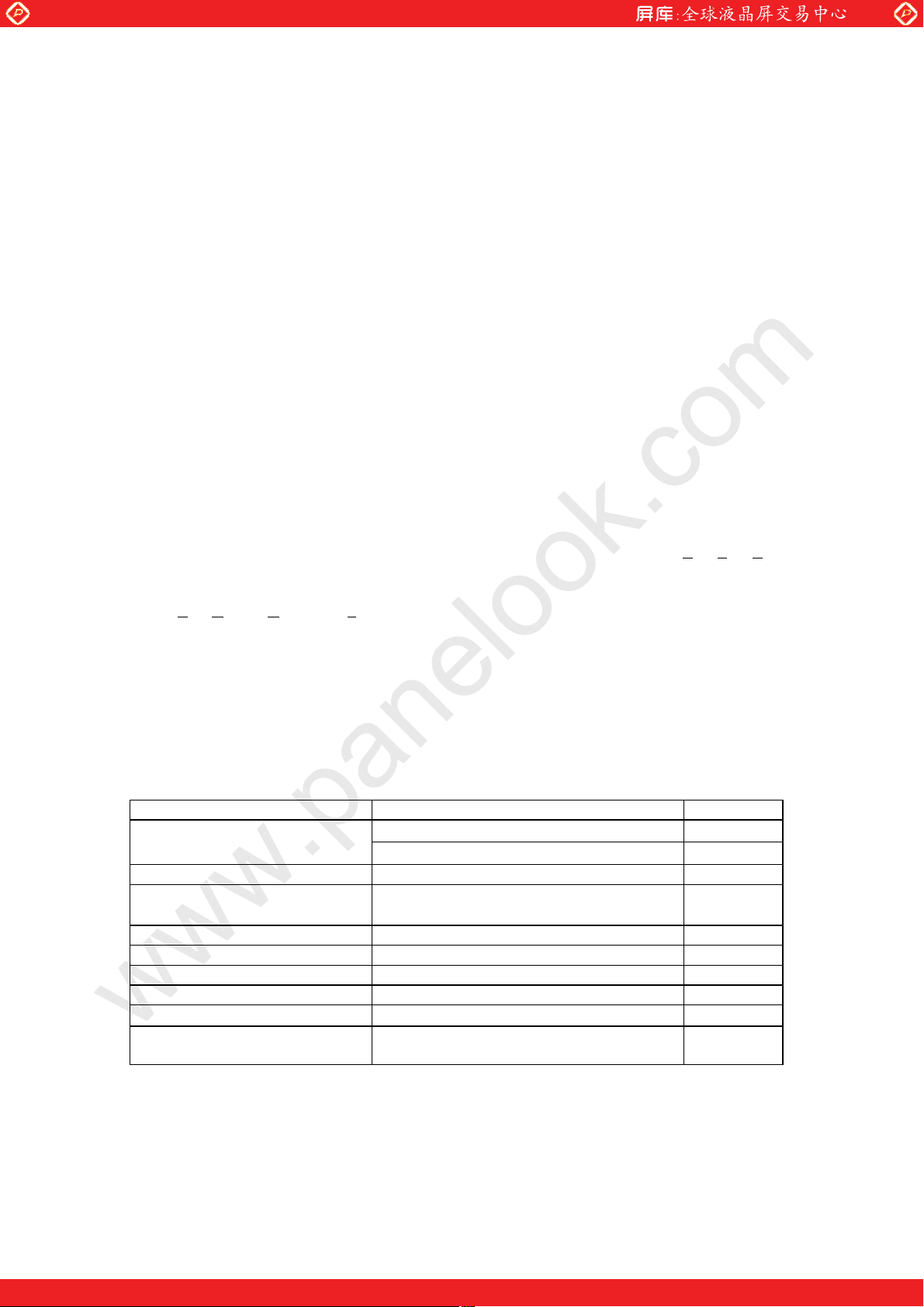
3. Mechanical Specifications
Parameter Specifications Unit
Display size
Active area 1152.0(H) x 648.0 (V) mm
Pixel Format
Pixel pitch 0.600(H) x 0.600 (V) mm
Pixel configuration R, G, B vertical stripe
Display mode Normally black
Unit Outline Dimensions (*1) 1219.0(W) x 706.7(H) x 64.6(D) mm
Mass
Surface treatment
(*1) Outline dimensions are shown in Fig.1 (excluding protruding portion)
www.panelook.com
132.174 㧔Diagonal㧕
52.0 㧔Diagonal㧕
1920(H) x 1080(V)
㧔1pixel = R + G + B dot㧕
21.0 r1.0
Anti glare
Hard coating: 2H
LD- 20125A-1
one billion
cm
inch
pixel
kg
colors by
One step solution for LCD / PDP / OLED panel application: Datasheet, inventory and accessory!
www.panelook.com
Page 4
Global LCD Panel Exchange Center
4. Input Terminals
4.1. TFT panel driving
CN1 (Interface signals and +12V DC power supply)
Using connector : FI-RE51S-HF (Japan Aviation Electronics Ind. , Ltd.)
Mating connector : FI-RE51HL, FI-RE51CL (Japan Aviation Electronics Ind. , Ltd.)
Mating LVDS transmitter : THC63LVD1023 or equivalent device
Pin No. Symbol Function Remark
1
2
3
4
5 Reserved
6 Reserved
7 SELLVDS
8 Reserved
9
10
11 GND
12
13
14
15
16
17
18
19
20
21
22
23
24
25
26
27
28
29
30
31
32
33
34
35
36
37
38
39
40
41
42
43
44
GND
Reserved It is required to set non-connection(OPEN)
Reserved It is required to set non-connection(OPEN)
Reserved It is required to set non-connection(OPEN)
It is required to set non-connection(OPEN)
It is required to set non-connection(OPEN)
Select LVDS data order [Note1,2]
It is required to set non-connection(OPEN)
O/S set O/S operation setting H:O/S_ON, L:O/S_OFF [Note 3]
FRAME
AIN0- Aport (-)LVDS CH0 differential data input
AIN0+ Aport (+)LVDS CH0 differential data input
AIN1- Aport (-)LVDS CH1 differential data input
AIN1+ Aport (+)LVDS CH1 differential data input
AIN2- Aport (-)LVDS CH2 differential data input
AIN2+ Aport (+)LVDS CH2 differential data input
GND
ACK- Aport LVDS Clock signal(-)
ACK+ Aport LVDS Clock signal(+)
GND
AIN3- Aport (-)LVDS CH3 differential data input
AIN3+ Aport (+)LVDS CH3 differential data input
AIN4- Aport (-)LVDS CH4 differential data input
AIN4+ Aport (+)LVDS CH4 differential data input
GND
GND
BIN0- Bport (-)LVDS CH0 differential data input
BIN0+ Bport (+)LVDS CH0 differential data input
BIN1- Bport (-)LVDS CH1 differential data input
BIN1+ Bport (+)LVDS CH1 differential data input
BIN2- Bport (-)LVDS CH2 differential data input
BIN2+ Bport (+)LVDS CH2 differential data input
GND
BCK- Bport LVDS Clock signal(-)
BCK+ Bport LVDS Clock signal(+)
GND
BIN3- Bport (-)LVDS CH3 differential data input
BIN3+ Bport (+)LVDS CH3 differential data input
BIN4- Bport (-)LVDS CH4 differential data input
BIN4+ Bport (+)LVDS CH4 differential data input
GND
GND
GND
Frame frequency setting 1:60Hz 0:50Hz
www.panelook.com
(Shown in Fig.1)
LD- 20125A-2
ًA
Pull up 3.3V
Pull up 3.3V
Pull up 3.3V
Pull down : (GND)
Pull down : (GND)
Pull down : (GND)
Pull down : (GND)
Pull up 3.3V
Pull down :GND
One step solution for LCD / PDP / OLED panel application: Datasheet, inventory and accessory!
www.panelook.com
Page 5
Global LCD Panel Exchange Center
45
46
47
48
49
50
51
[note]GND of a liquid crystal panel drive part has connected with a module chassis.
GND
GND
VCC +12V Power Supply
VCC +12V Power Supply
VCC +12V Power Supply
VCC +12V Power Supply
VCC +12V Power Supply
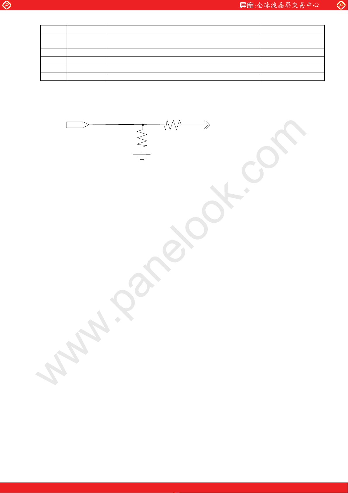
[Note 1]The equivalent circuit figure of the terminal
www.panelook.com
LD- 20125A-3
Te rm in al
10K
100
One step solution for LCD / PDP / OLED panel application: Datasheet, inventory and accessory!
www.panelook.com
Page 6
Global LCD Panel Exchange Center
[Note 2] LVDS Data order
SELLVDS
Data L(GND) or Open
TA0
TA1
TA2
TA3
TA4
TA5
TA6
TB0
TB1
TB2
TB3
TB4
TB5
TB6
TC0
TC1
TC2
TC3
TC4 NA NA
TC5 NA NA
TC6 DE(*) DE(*)
TD0
TD1
TD2
TD3
TD4
TD5
TD6
TE0
TE1
TE2
TE3
TE4
TE5
TE6
NA: Not Available
(*)Since the display position is prescribed by the rise of DE(Display Enable)signal, please do not fix DE
signal during operation at ”High”.
R2㩷
R3㩷
R4㩷
R5㩷
R6㩷
R7㩷
G2㩷
G3㩷
G4㩷
G5㩷
G6㩷
G7㩷
B2㩷
B3㩷
B4㩷
B5㩷
B6㩷
B7㩷
R8㩷
R9(MSB)㩷
G8㩷
G9(MSB)㩷
B8㩷
B9(MSB)㩷
NA
R0(LSB)㩷
R1㩷
G0(LSB)㩷
G1㩷
B0(LSB)㩷
B1㩷
NA㩷
www.panelook.com
LD- 20125A-4
H(3.3V)
R4
R5
R6
R7
R8
R9(MSB)
G4
G5
G6
G7
G8
G9(MSB)
B4
B5
B6
B7
B8
B9(MSB)
R2
R3
G2
G3
B2
B3
㩷
N/A
R0(LSB)
R1
G0(LSB)
G1
B0(LSB)
B1
N/A
One step solution for LCD / PDP / OLED panel application: Datasheet, inventory and accessory!
www.panelook.com
Page 7
Global LCD Panel Exchange Center
–
,
–
SELLVDS= Low (GND) or OPEN
ACK+,BCK+
ACK– ,BCK–
AIN0+,BIN0+
AIN0
BIN0
AIN1+,BIN1+
AIN1
–,BIN1–
AIN2+,BIN2+
AIN2
–,BIN2–
AIN3+,BIN3+
–,BIN3–
AIN3
AIN4+,BIN4+
AIN4
–,BIN4–
www.panelook.com
ًA
1 cycle
G2 R7 R6 R5 R4 R3 R2 R2 R3 G2
B3 B2 G7 G6 G5 G4 G3 G3 G4 B3
DE
NA NA
B9 B8 G9 G8 R9 R8 R8 R9 NA NA
B1 B0 G1 G0 R1 R0 R0 R1 NA NA
B7 B6 B5 B4 B4 B5
LD- 20125A-5
DE
SELLVDS= High (3.3V)
ACK+,BCK+
ACK– ,BCK–
AIN0+,BIN0+
AIN0
–,BIN0–
AIN1+,BIN1+
AIN1
–,BIN1–
AIN2+,BIN2+
AIN2
–,BIN2–
AIN3+,BIN3+
AIN3
–,BIN3–
AIN4+,BIN4+
–,BIN4–
AIN4
1 cycle
G4 R9 R8 R7 R6 R5 R4 R4 R5 G4
B5 B4 G9 G8 G7 G6 G5 G5 G6 B5
DE
NA NA
B3 B2 G3 G2 R3 R2 R2 R3 NA NA
B1 B0 G1 G0 R1 R0 R0 R1 NA NA
B9 B8 B7 B6 B6 B7
DE
DE: Display Enable, NA: Not Available (Fixed Low)
One step solution for LCD / PDP / OLED panel application: Datasheet, inventory and accessory!
www.panelook.com
Page 8
Global LCD Panel Exchange Center
V
㪠㪥㪧㪬㪫㩷㪪㪠㪞㪥㪘㪣㪪㩷
㪦㪆㪪㩷㪚㪦㪥㪫㪩㪦㪣
㩷
㩷 㪪㪠㪞㪥㪘㪣㪪
㩷
㪧㪦㪮㪜㪩㩷㪪㪬㪧㪧㪣㪰㩷
㩷
㩷
㩷
㩷
㪣㪚㪛㩷㪧㪘㪥㪜㪣㩷
㪈㪐㪉㪇㬍㪊㩿㪩㪞㪙㪀㬍㪈㪇㪏㪇㩷
㪞㪘㪫㪜㩷㪛㪩㪠㪭㪜㪩㩷
㪞㪘㪫㪜㩷㪛㪩㪠㪭㪜㪩㩷
㪚㪦㪥㪫㪩㪦㪣㩷㪧㪮㪙㩷
㪠㪥㪭㪜㪩㪫㪜㪩㩷
㪠㪥㪧㪬㪫㩷
㪪㪠㪞㪥㪘㪣㪪㩷
㪧㪦㪮㪜㪩㩷㪪㪬㪧㪧㪣㪰㩷
㪪㪦㪬㪩㪚㪜 㪛㪩㪠㪭㪜㪩
㪙㪘㪚㪢㩷 㪣㪠㪞㪟㪫㩿㪚㪚㪝㪫㬍㪉㪋㪀㩷
[Note 3] The equivalent circuit figure of the terminal
Te rm in al
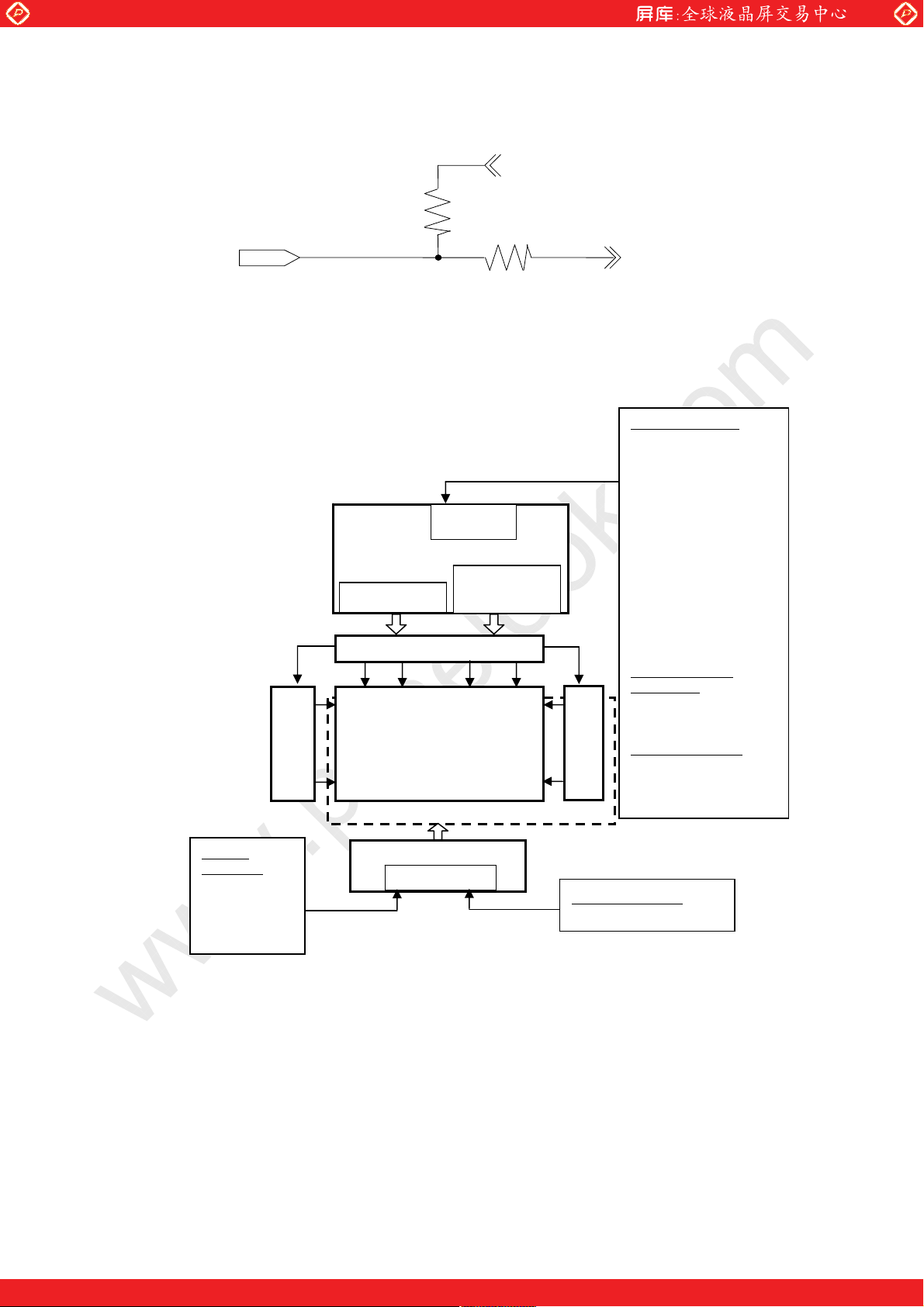
4.2. Interface block diagram
㪭㫆㫅㪆㫆㪽㪽㩷
㪧㪻㫀㫄㩷
㪧㪻㫀㫄㪶㫊㪼㫃㩷
www.panelook.com
㩷
㩷
㪚㫆㫅㫋㫉㫆㫃㩷
3.3
4.7K
100
㪚㪥㪈㩷
㪧㫆㫎㪼㫉㩷㪪㫌㫇㫇㫃㫐
㪚㫀㫉㪺㫌㫀㫋㩷
㪪㪜㪣㪣㪭㪛㪪㩷 㩷
㪘㪠㪥㪇㪄㩷㪘㪠㪥㪇㪂㩷
㪘㪠㪥㪈㪄㩷㪘㪠㪥㪈㪂㩷
㪘㪠㪥㪉㪄㩷㪘㪠㪥㪉㪂㩷
㪘㪠㪥㪊㪄㩷㪘㪠㪥㪊㪂㩷
㪘㪠㪥㪋㪄㩷㪘㪠㪥㪋㪂㩷
㪘㪚㪢㪄㩷㪘㪚㪢㪂㩷
㪙㪠㪥㪇㪄㩷㪙㪠㪥㪇㪂㩷
㪙㪠㪥㪈㪄㩷㪙㪠㪥㪈㪂㩷
㪙㪠㪥㪉㪄㩷㪙㪠㪥㪉㪂㩷
㪙㪠㪥㪊㪄㩷㪙㪠㪥㪊㪂㩷
㪙㪠㪥㪋㪄㩷㪙㪠㪥㪋㪂㩷
㪙㪚㪢㪄㩷㪙㪚㪢㪂㩷
㩷
㩷
㪦㪆㪪㩷㪪㪜㪫㩷
㪝㪩㪘㪤㪜㩷
㩷
㩷 㩷 㪂㪈㪉㪭㩷㪛㪚㩷
㩷 㩷 㪂㪉㪋㪭㩷㪛㪚㩷
LD- 20125A-6
One step solution for LCD / PDP / OLED panel application: Datasheet, inventory and accessory!
www.panelook.com
Page 9

Global LCD Panel Exchange Center
4.3. Backlight driving
CN103 (+24V DC power supply and inverter control)
Using connector: S14B-PH-K-S (LF) (JST)
Mating connector: PHR-14 (JST)
Pin No. Symbol Function Default(OPEN) Input Impedance Remark
1 VINV +24V -
2 VINV +24V -
3 VINV +24V -
4 VINV +24V -
5 VINV +24V -
6 GND -
7 GND -
8 GND -
9 GND -
10 GND -
11 Reserved For LCD module internal
12 VON Inverter ON/OFF GND : pull down
13 VBRT Brightness Control 3.3V : pull up
14 VBRT_sel Brightness Control
*GND of an inverter board is not connected to GND of a module chassis and a liquid crystal panel drive part.
CN104(+24V DC power supply)
Using connector: S14B-PH-K-S(LF) (JST)
Mating connector: PHR-14 (JST)
Pin No. Symbol Function Default(OPEN) Input Impedance Remark
1 VINV +24V -
2 VINV +24V -
3 VINV +24V -
4 VINV +24V -
5 VINV +24V -
6 GND -
7 GND -
8 GND -
9 GND -
10 GND -
11 Reserved For LCD module internal
12 Reserved For LCD module internal
13 Reserved For LCD module internal
14 Reserved For LCD module internal
[Note 1] Inverter ON/OFF
Input voltage Function
0V Inverter : OFF
3.3V Inverter : ON
www.panelook.com
usage, should be open
selection
usage, should be open
usage, should be open
usage, should be open
usage, should be open
Inverter OFF
Brightness 100%
3.3V : pull up
Selected Analog PWM
-
-
LD- 20125A-7
22K ohm [Note 1]
100K ohm [Note 3]
100K ohm [Note 2]
One step solution for LCD / PDP / OLED panel application: Datasheet, inventory and accessory!
www.panelook.com
Page 10

Global LCD Panel Exchange Center
[Note 2] Brightness Control selection
Pin No.14 is used for the selection of dimming control for V
Input voltage V
0V Pulse dimming
3.3V Analog dimming
[Note 3]Brightness Control
1. Analog Dimming
Brightness control is regulated by analog input voltage (0V to 3.3V).
Input voltage [V
[Reference]
Brightness ratio㨇%㨉
[Note] PWM frequency : 275r10Hz
[Note]There is a case that lamp mura may happen, depending on ambient temperature and dimming.
Dimming level should be set according to your evaluation of actual display performance.
(Minimum input voltage 1.5V at below 15)
2.Pulse Dimming
Pin No.13 is used for the control of the PWM duty with input pulse from 150Hz to 350Hz.
BRT
www.panelook.com
LD- 20125A-8
BRT pin (Pin No.13).
BRT
Ta=25
MIN TYP MAX Function
]
0V <-> 3.3V
20 <-> 100
0V: Dark - 3.3V: Bright
㪠㫅㫇㫌㫋㩷㪧㪮㪤㩷㫎㪸㫍㪼㪽㫆㫉㫄㩷
㪟㫀㪾㪿㩷㫍㫆㫃㫋㪸㪾㪼㩷
㪣㫆㫎㩷㫍㫆㫃㫋㪸㪾㪼㩷
㪫㫆㫅㩷
㪦㪥㩷 㪦㪥㩷㪦㪝㪝㩷
㪫㩷
Duty㧩TON/T
Pulse signal [Hz]
MIN TYP MAX
150 275 350
DUTY(TON/T) [%] 35 <-> 100
Dimming level
[%] 20 <-> 100
(Brightness ratio)
Pulse signal=275Hz
Remark
Ta=25
Ta=25
[Note]There is a case that lamp mura may happen, depending on ambient temperature,
in dimming. Minimum dimming level should be set according to your evaluation of
actual display performance. (Minimum duty 60㧑 at below 15)
[Note]In case of using Pulse Dimming, be careful so that the V
signal (Pin 13) doesn’t have glitch.
BRT
One step solution for LCD / PDP / OLED panel application: Datasheet, inventory and accessory!
www.panelook.com
Page 11

Global LCD Panel Exchange Center
4.4. The back light system characteristics
The back light system is direct type with 24 CCFTs (Cold Cathode Fluorescent Tube).
The characteristics of the lamp are shown in the following table. The value mentioned below is at the case of one
CCFT.
Item Symbol Min. Typ. Max. Unit Remarks
Life time TL - 60000 - Hour [Note]
[Note]
x Lamp life time is defined as the time when brightness becomes 50% of the original value in the continuous
operation under the condition of Ta=25qC and brightness control=100%.
x Above value is applicable when the long side of LCD module is placed horizontally (Landscape position).
(Lamp lifetime may vary if LCD module is in portrait position due to the change of mercury density inside
the lamp.)
5. Absolute Maximum Ratings
Parameter Symbol Condition Ratings Unit Remark
Input voltage
(for Control)
12V supply voltage
(for Control)
Input voltage
(for Inverter)
24V supply voltage
(for Inverter)
VCC
V
P
P
dim
V
I
V
ON
dim;
_sel
INV
www.panelook.com
Ta=25 qC
Ta=25 qC
Ta=25 qC
Ta=25 qC
LD- 20125A-9
-0.3 ~ 3.6 V [Note 1]
0 ~ + 14 V
0 ~ + 6 V
0 ~ +29 V
Storage temperature Tstg - -25 ~ +60
Operation temperature
(Ambient)
Topa - 0 ~ +50
[Note 1] SELLVDS, FRAME, O/S_set,
[Note 2] Humidity 95%RH Max.(Ta҇40qC)
Maximum wet-bulb temperature at 39 qC or less.(Ta>40qC)
No condensation.
qC
[Note 2]
qC
One step solution for LCD / PDP / OLED panel application: Datasheet, inventory and accessory!
www.panelook.com
Page 12

Global LCD Panel Exchange Center
6. Electrical Characteristics
6.1. Control circuit driving Ta=25 qC
Parameter Symbol Min. Typ. Max. Uniit Remark
Supply voltage Vcc 11.4 12 12.6 V [Note 1]
+12V supply
voltage
Permissible input ripple voltage VRP - - 100 mVP-P Vcc = +12.0V
threshold voltage
Input High voltage VIH 2.3 - 3.3 V
Input leak current (Low)
Input leak current (High)
[Note]VCM: Common mode voltage of LVDS driver.
[Note 1]
Input voltage sequences Dip conditions for supply voltage
0 < t1 ҇ 20ms a) 6.5V ҇ Vcc < 10.8V
10 < t2 ҇ 20ms td ҇ 10ms
10 < t3 ҇ 50ms b) Vcc < 6.5V
0 < t4 ҇ 1s Dip conditions for supply voltage is
t5 ҈ 200ms based on input voltage sequence.
t6 ҈ 0
t7 ҈ 300ms
Current dissipation Icc - 0.8 2.0 A [Note 2]
Inrush current
High VTH - - 100 mV Differential input
Low V
Input Low voltage VIL 0 - 1.0 V
Terminal resistor RT - 100 -
www.panelook.com
LD- 20125A-10
I
- 4.6 - A
RUSH
- 0.3 - ms
T
RUSH
TL -100 - - mV
IIL1 - - 400 μA
IL2 - - 40 μA
I
IIH1 - - 40 μA
I
IH2 - - 400 μA
:
[Note 7]
V
CM = +1.2V
[Note 6]
[Note 3]
I = 0V
V
[Note 4]
I = 0V
V
[Note 5]
I = 3.3V
V
[Note 4]
I = 3.3V
V
[Note 5]
Differential
input
0.9VCC
0.1Vcc
Vcc
Data1
Data2
Back light:V
t1
t2
ON
t3
INV
t5
OFF
t6
t4
t3
0.9Vcc
0.1Vcc
t7
OFF
Vcc
0.1Vcc
V1
V2
td
Data1: ACKr, AIN0r, AIN1r, AIN2r, AIN3r, AIN4r,BCKr, BIN0r, BIN1r, BIN2r, BIN3r, BIN4
*V
voltage pursues the sequence mentioned above
CM
Data2: SELLVDS, FRAME, O/S_SET
V1:10.8V
V2:6.5V
One step solution for LCD / PDP / OLED panel application: Datasheet, inventory and accessory!
www.panelook.com
Page 13

Global LCD Panel Exchange Center
[Note]About the relation between data input and back light lighting, please base on the above-mentioned input
sequence. When back light is switched on before panel operation or after a panel operation stop, it may not
display normally. But this phenomenon is not based on change of an incoming signal, and does not give
damage to a liquid crystal display.
[Note 2] Typical current situation: 256 gray-bar patterns. (Vcc = +12.0V)
The explanation of RGB gray scale is seen in section 8.
4)$
)5
4)$
)5
4)$
)5
[Note 3] SELLVDS, FRAME, O/S_SET
[Note 4] O/S_SET
[Note 5] FRAME, SELLVDS
[Note 6] ACKr, AIN0r, AIN1r, AIN2r, AIN3r, AIN4r,BCKr, BIN0r, BIN1r, BIN2r, BIN3r, BIN4
[Note 7] Vcc12V inrush current waveform
t1 = 500us
Irush = 4.6A
Trush = 300us
4)$
)5
www.panelook.com
4)$
)5
CK㧩74.25MHz
Th㧩14.8s
LD- 20125A-11
Vcc㧩+12.0V
Vcc
Icc
One step solution for LCD / PDP / OLED panel application: Datasheet, inventory and accessory!
www.panelook.com
Page 14

Global LCD Panel Exchange Center
V
V
V
V
6.2. Inverter driving for back light
The back light system is
direct type with 24 CCFTs (Cold Cathode Fluorescent Tube).
Parameter Symbol Min. Typ. Max. Unit Remark
www.panelook.com
LD- 20125A-12
㧗24V
Current dissipation 1 IINV 1 - 11.8 13.0 A
Current dissipation 2 IINV 2 - 10.3 11.5 A
VINV = 24V, Ta=25qC
Brightness Control
= 100%
[Note 1,2]
Supply voltage VINV 22.8 24.0 25.2 V
Permissible input ripple voltage VRF - - 300 V VINV = +24.0V
Input voltage (Low) V
Input voltage (High) V
0 - 1.0 V
ONL
2.3 - 3.6 V
ONH
, P
V
ON
dim;,Pdim
_sel
[Note 1] 1) VINV-turn-on condition
INV
1.0V
21.6V
T1㧪100Ps
҈1ms
T2
T1 T2
ON,VBRT
0V
2.0V
2) V
INV-turn-off condition
, V
BRT
t1҈1ms
ON
t1
INV
1.0V
0V
21.6V
0V
[Note 2] Current dissipation 1 : Definition within 60 minutes after turn on. (Rush current is excluded.)
Current dissipation 2 : Definition more than 60minutes after turn on.
One step solution for LCD / PDP / OLED panel application: Datasheet, inventory and accessory!
www.panelook.com
Page 15

Global LCD Panel Exchange Center
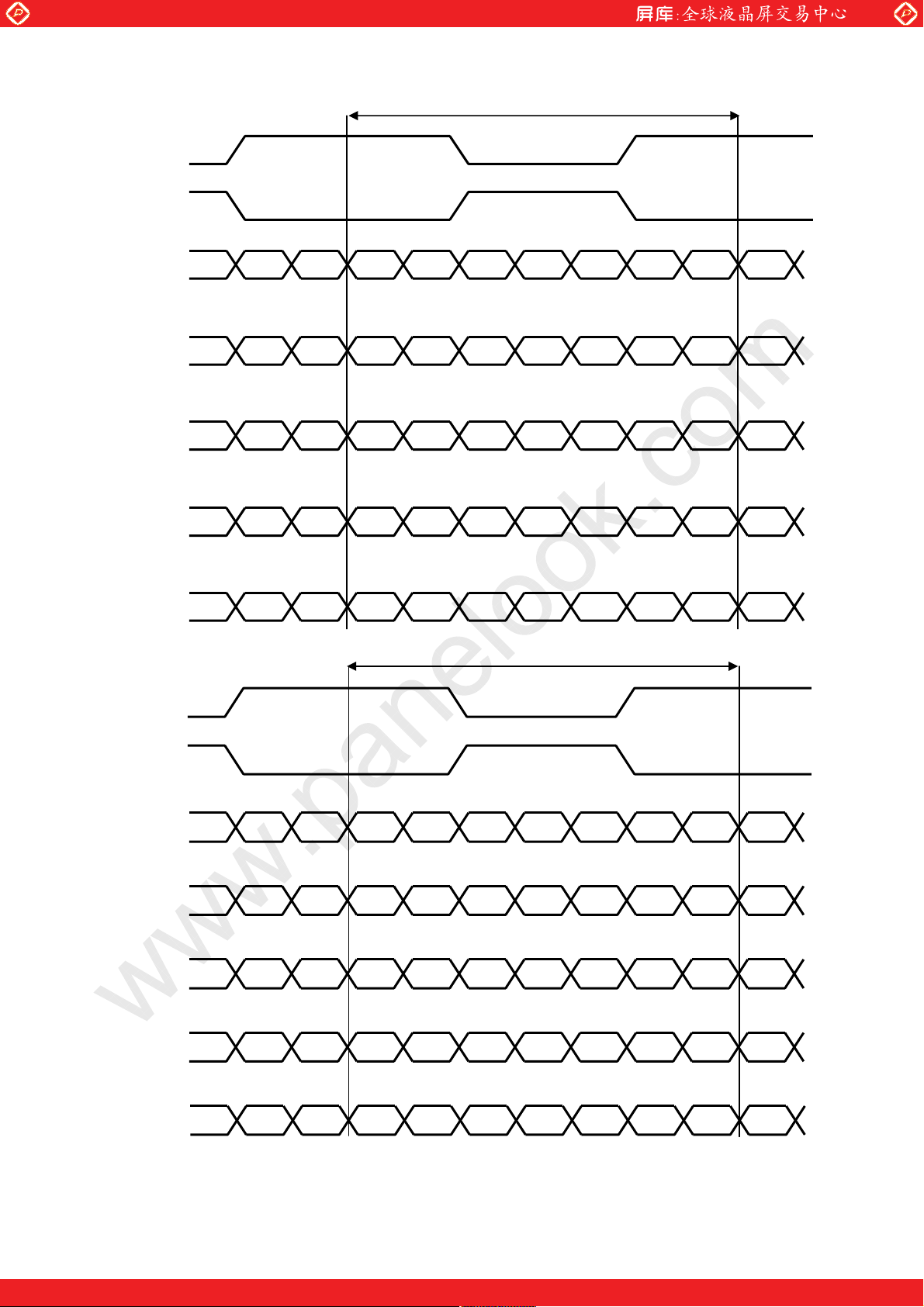
7. Timing characteristics of input signals
7.1. Timing characteristics
Timing diagrams of input signal are shown in Fig.2.
Parameter Symbol Min. Typ. Max. Unit Remark
Clock Frequency 1/Tc 67 74.25 76 MHz
Horizontal period TH
Data enable
signal
[Note]-When vertical period is very long, flicker and etc. may occur.
-Please turn off the module after it shows the black screen.
-Please make sure that length of vertical period should become of an integral multiple of horizontal
length of period. Otherwise, the screen may not display properly.
-As for your final setting of driving timing, we will conduct operation check test at our side, please
inform your final setting.
DE
Aport DATA
(R,G,B)
Bport DATA
(R,G,B)
DE
Horizontal period (High) THd 960 960 960 clock
Vertical period TV 1109 1125 1200 line
Vertical period (High) TVd 1080 1080 1080 line
1919
Tc
www.panelook.com
1050 1100 1200 clock
14.2 14.8 16.1 μs
TH
THd
1
2
TV
3
4 1920 1920
1 2 1080
Fig.2 Timing characteristics of input signals
1919
1079
TVd
LD- 20125A-13
One step solution for LCD / PDP / OLED panel application: Datasheet, inventory and accessory!
www.panelook.com
Page 16

Global LCD Panel Exchange Center
7.2. Input data signal and display position on the screen
㩷
R1㩷 G1㩷 B1㩷 R2㩷 G2㩷 B2
㧝㨮㧝㩷 㧝㧞㩷
www.panelook.com
LD- 20125A-14
㧝㧝㩷 㧝㧞㩷 㧝㧟
㧞㧝㧞㧞
㧟㧝㩷
㨯㩷
R㩷 G㩷B㩷
Display position of Dat (V,H)
㨯
㨯
㩷
One step solution for LCD / PDP / OLED panel application: Datasheet, inventory and accessory!
www.panelook.com
Page 17

Global LCD Panel Exchange Center
8. Input Signal, Basic Display Colors and Gray Scale of Each Color
Colors &
Gray scale
Black – 0 0 0 0 0 0 0 0 0 0 0 0 0 0 0 0 0 0 0 0 0 0 0 0 0 0 0 0 0 0
Blue – 0 0 0 0 0 0 0 0 0 0 0 0 0 0 0 0 0 0 0 0 1 1 1 1 1 1 1 1 1 1
Green – 0 0 0 0 0 0 0 0 0 0 1 1 1 1 1 1 1 1 1 1 0 0 0 0 0 0 0 0 0 0
Cyan – 0 0 0 0 0 0 0 0 0 0 1 1 1 1 1 1 1 1 1 1 1 1 1 1 1 1 1 1 1 1
Red – 1 1 1 1 1 1 1 1 1 1 0 0 0 0 0 0 0 0 0 0 0 0 0 0 0 0 0 0 0 0
Basic Color
Magenta – 1 1 1 1 1 1 1 1 1 1 0 0 0 0 0 0 0 0 0 0 1 1 1 1 1 1 1 1 1 1
Yellow – 1 1 1 1 1 1 1 1 1 1 1 1 1 1 1 1 1 1 1 1 0 0 0 0 0 0 0 0 0 0
White – 1 1 1 1 1 1 1 1 1 1 1 1 1 1 1 1 1 1 1 1 1 1 1 1 1 1 1 1 1 1
Black GS0 0 0 0 0 0 0 0 0 0 0 0 0 0 0 0 0 0 0 0 0 0 0 0 0 0 0 0 0 0 0
× GS1 1 0 0 0 0 0 0 0 0 0 0 0 0 0 0 0 0 0 0 0 0 0 0 0 0 0 0 0 0 0
R0 R1 R2 R3 R4 R5 R6 R7 R8 R9 G0 G1 G2 G3 G4 G5 G6 G7 G8 G9 B0 B1 B2 B3 B4 B5 B6 B7 B8 B9
Gray
Scale
www.panelook.com
LD- 20125A-15
Data signal
Darker GS2 0 1 0 0 0 0 0 0 0 0 0 0 0 0 0 0 0 0 0 0 0 0 0 0 0 0 0 0 0 0
×
Ø
Brighter GS1021 1 0 1 1 1 1 1 1 1 1 0 0 0 0 0 0 0 0 0 0 0 0 0 0 0 0 0 0 0 0
p
p
p
p
p
p
p
p
Gray Scale of Red
Ø GS1022 0 1 1 1 1 1 1 1 1 1 0 0 0 0 0 0 0 0 0 0 0 0 0 0 0 0 0 0 0 0
Red GS1023 1 1 1 1 1 1 1 1 1 1 0 0 0 0 0 0 0 0 0 0 0 0 0 0 0 0 0 0 0 0
Black GS0 0 0 0 0 0 0 0 0 0 0 0 0 0 0 0 0 0 0 0 0 0 0 0 0 0 0 0 0 0 0
× GS1 0 0 0 0 0 0 0 0 0 0 1 0 0 0 0 0 0 0 0 0 0 0 0 0 0 0 0 0 0 0
Darker GS2 0 0 0 0 0 0 0 0 0 0 0 1 0 0 0 0 0 0 0 0 0 0 0 0 0 0 0 0 0 0
×
Ø
Brighter GS1021 0 0 0 0 0 0 0 0 0 0 1 0 1 1 1 1 1 1 1 1 0 0 0 0 0 0 0 0 0 0
Gray Scale of Green
Ø GS1022 0 0 0 0 0 0 0 0 0 0 0 1 1 1 1 1 1 1 1 1 0 0 0 0 0 0 0 0 0 0
Green GS1023 0 0 0 0 0 0 0 0 0 0 1 1 1 1 1 1 1 1 1 1 0 0 0 0 0 0 0 0 0 0
Black GS0 0 0 0 0 0 0 0 0 0 0 0 0 0 0 0 0 0 0 0 0 0 0 0 0 0 0 0 0 0 0
× GS1 0 0 0 0 0 0 0 0 0 0 0 0 0 0 0 0 0 0 0 0 1 0 0 0 0 0 0 0 0 0
Darker GS2 0 0 0 0 0 0 0 0 0 0 0 0 0 0 0 0 0 0 0 0 0 1 0 0 0 0 0 0 0 0
Ø
Ø
Brighter GS1021 0 0 0 0 0 0 0 0 0 0 0 0 0 0 0 0 0 0 0 0 1 0 1 1 1 1 1 1 1 1
Gray Scale of Blue
Ø GS1022 0 0 0 0 0 0 0 0 0 0 0 0 0 0 0 0 0 0 0 0 0 1 1 1 1 1 1 1 1 1
p
p
p
p
p
p
p
p
p
p
p
p
p
p
p
p
Blue GS1023 0 0 0 0 0 0 0 0 0 0 0 0 0 0 0 0 0 0 0 0 1 1 1 1 1 1 1 1 1 1
0: Low level voltage, 1: High level voltage.
Each basic color can be displayed in 1024 gray scales from 10 bits data signals. According to the combination of
total 30 bits data signals, the TBD-color display can be achieved on the screen.
One step solution for LCD / PDP / OLED panel application: Datasheet, inventory and accessory!
www.panelook.com
Page 18

Global LCD Panel Exchange Center
9. Optical characteristics
Parameter Symbol Condition Min. Typ. Max. Unit Remark
Viewing angle
range
Contrast ratio CRn 1000 1500 - [Note2,4]
Response time
Chromaticity
Luminance White 360 450 - -
Luminance
uniformity
Measurement condition: Set the value of V
*The measurement shall be executed 60 minutes after lighting at rating.
[Note]The optical characteristics are measured using the following equipment.
Detector㧔EZ-CONTRAST/ Photodiode㧕
Fig.4-1 Measurement of viewing angle range and
Horizontal
Vertical
White
Red
Green
Blue
White
Middle of the screen (T㧩0q)
TFT-LCD Module
Response time.
Viewing angle range: EZ-CONTRAST
Response time: Photodiode
www.panelook.com
Ta=25qC, Vcc=12.0V, VINV =24.0V, V
T
T
T
T
21
22
11
12
W
r
W
d
CR҈10
70 88 - Deg.
70 88 -
- 6 - ms [Note3,4,5]
x 0.242 0.272 0.302 y 0.247 0.277 0.307 x 0.610 0.640 0.670 -
T
y 0.300 0.330 0.360 -
=0 deg.
x 0.250 0.280 0.310 y 0.570 0.600 0.630 x 0.120 0.150 0.180 y 0.030 0.060 0.090 -
Gw
to maximum luminance of white.
BRT
- - 1.25 cd/m
400mm
Field=1q
Middle of the screen (T㧩0q)
TFT-LCD Module
Fig.4-2 Measurement of Contrast, Luminance,
Chromaticity.
=100%㧘Timing:60Hz(typ. value)
BRT
Deg.
Detector㧔SR-3㧕
LD- 20125A-16
[Note1,4]
[Note4]
2
[Note 6]
One step solution for LCD / PDP / OLED panel application: Datasheet, inventory and accessory!
www.panelook.com
Page 19

Global LCD Panel Exchange Center
[Note 1]Definitions of viewing angle range :
T
22
T
12
[Note 2]Definition of contrast ratio :
The contrast ratio is defined as the following.
Luminance (brightness) with all pixels white
Contrast Ratio
Luminance (brightness) with all pixels black
[Note 3]Definition of response time
The response time (W
and Wr) is defined as the following figure and shall be measured by switching the input
d
signal for “any level of gray (0%, 25%, 50%, 75% and 100%)” and “any level of gray (0%, 25%, 50%, 75%
and 100%)”.
www.panelook.com
Normal line
T
11
6 o’clock direction
㧩
T
LD- 20125A-17
21
0%
0%
25㧑
50㧑
75㧑
100%
td: 25%-0㧑
td: 50%-0㧑 td: 50%-25㧑
td: 75%-0㧑 td: 75%-25㧑 td: 75%-50㧑
td: 100%-0㧑 td: 100%-25㧑 td: 100%-50㧑 td:100%-75㧑
25㧑 50㧑 75㧑
tr:0%-25㧑
tr:0%-50% tr:0%-75% tr:0%-100%
tr: 25%-50㧑 tr25%-75㧑 tr: 25%-100㧑
tr: 50%-75㧑 tr: 50%-100㧑
100%
tr: 75%-100㧑
t*:x-y...response time from level of gray(x) to level of gray(y)
W
= 6(tr:x-y)/10 , Wd = 6(td:x-y)/10
r
Bright
100%
90%
Dark
Bright
Photodetector
10%
Output
0%
Wd Wr
time
[Note 4]This shall be measured at center of the screen.
[Note 5] This value is valid when O/S driving is used at typical input time value.
One step solution for LCD / PDP / OLED panel application: Datasheet, inventory and accessory!
www.panelook.com
Page 20

Global LCD Panel Exchange Center
[Note 6]Definition of white uniformity ;
White uniformity is defined as the following with five measurements. (AaE)
Maximum luminance of five points (brightness)
㨃㧩
G
Minimum luminance of five points (brightness)
10. Handling Precautions of the module
a) Be sure to turn off the power supply when inserting or disconnecting the cable.
b) This product is using the parts (inverter, CCFT etc), which generate the high voltage.
Therefore, during operating, please don't touch these parts.
c) Brightness control voltage is switched for “ON” and “OFF”, as shown in Fig.4. Voltage difference generated
by this switching, 'V
inverter and its surrounding circuit. So, separate the power supply of the inverter circuit with the one of its
surrounding circuit.
INV, may affect a sound output, etc. when the power supply is shared between the
www.panelook.com
480
960 1440
A㩷
C㩷
B㩷
LD- 20125A-18
pixel
D㩷
E㩷
270
540
810
pixel
㩷
㰱VINV㩷
VINV㩷
IINV㩷
PWM control
signal㩷
0V㩷
0A㩷
ON㩷 ON㩷OFF㩷
0V㩷
Fig.4 Brightness control voltage.
*Since inverter board’s GND is not connected to the frame of the LCD module, please connect it with the
Customer’s GND of inverter power supply.
d) Be sure to design the cabinet so that the module can be installed without any extra stress such as warp or
twist.
e) Since the front polarizer is easily damaged, pay attention not to scratch it.
f) Since long contact with water may cause discoloration or spots, wipe off water drop immediately.
g) When the panel surface is soiled, wipe it with absorbent cotton or other soft cloth.
h) Since the panel is made of glass, it may break or crack if dropped or bumped on hard surface. Handle with
care.
One step solution for LCD / PDP / OLED panel application: Datasheet, inventory and accessory!
www.panelook.com
Page 21

Global LCD Panel Exchange Center
i) Since CMOS LSI is used in this module, take care of static electricity and take the human earth into
consideration when handling.
j) The module has some printed circuit boards (PCBs) on the back side, take care to keep them form any stress
or pressure when handling or installing the module; otherwise some of electronic parts on the PCBs may be
damaged.
k) Observe all other precautionary requirements in handling components.
l) When some pressure is added onto the module from rear side constantly, it causes display non-uniformity
issue, functional defect, etc. So, please avoid such design.
m) When giving a touch to the panel at power on supply, it may cause some kinds of degradation. In that case,
once turn off the power supply, and turn on after several seconds again, and that is disappear.
n) When handling LCD modules and assembling them into cabinets, please be noted that long-term storage in
the environment of oxidization or deoxidization gas and the use of such materials as reagent, solvent,
adhesive, resin, etc. which generate these gasses, may cause corrosion and discoloration of the LCD
modules.
o) This LCD module is designed to prevent dust from entering into it. However, there would be a possibility to
have a bad effect on display performance in case of having dust inside of LCD module. Therefore,
please ensure to design your TV set to keep dust away around LCD module.
11. Packing form
a) Piling number of cartons:2 maximum
b) Packing quantity in one carton:8pcs
c) Carton size:1320(W) 1110(D) 940(H)
d) Total mass of one carton filled with full modules:225kg(Max)
12. Reliability test item
No. Test item Condition
1
2
3
4
5
6
7
8
[Result evaluation criteria]
Under the display quality test condition with normal operation state, there shall be no change, which may
affect practical display function.
High temperature storage test
Low temperature storage test
High temperature and high humidity
operation test
High temperature operation test
Low temperature operation test
Vibration test
(non-operation)
Shock test
(non-operation)
ESD
www.panelook.com
Ta=60qC 240h
Ta=-25qC240h
Ta=40qC ; 95%RH 240h
(No condensation)
Ta=50qC 240h
Ta=0qC 240h
Frequency: 10~57Hz/Vibration width (one side): 0.075mm
: 58~500Hz/Acceleration: 9.8 m/s²
Sweep time: 11 minutes
Test period: 3 hours (1h for each direction of X, Y, Z)
Maximum acceleration: 294m/s
Pulse width: 11ms, sinusoidal half wave
Direction: +/-X, +/-Y, +/-Z, once for each direction.
* At the following conditions, it is a thing without incorrect
operation and destruction.
(1)Non-operation: Contact electric discharge r10kV
(2)Operation Contact electric discharge r8kV
Conditions: 150pF, 330ohm
LD- 20125A-19
2
Non-contact electric discharge r20kV
Non-contact electric discharge r15kV
One step solution for LCD / PDP / OLED panel application: Datasheet, inventory and accessory!
www.panelook.com
Page 22

Global LCD Panel Exchange Center
㧔
㧠㧿
㧕
LK520D3LZ88X(orT)
13. Others
1) Lot No. Label ;
The label that displays SHARP, product model (LK520D3LZ88), a product number is stuck on the back of the
module.
ޣ.-&.<:6ޤ05'%241&7%6+10
2) Packing Labe
ޣ.-&.<:6ޤ
␠ౝຠ⇟㧦
㧽㨡㨍㨚㨠㨕㨠㨥㧦
࡙ࠩຠ⇟
ࠪࡖࡊ‛ᵹ↪ࡌ࡞ߢߔޕ
3) Adjusting volume has been set optimally before shipment, so do not change any adjusted value.
If adjusted value is changed, the specification may not be satisfied.
4) Disassembling the module can cause permanent damage and should be strictly avoided.
5) Please be careful since image retention may occur when a fixed pattern is displayed for a long time.
A production year(the last figures of the Christian Era)
Bar code
㧸㨛㨠㧺㧻㧚
Bar code
Bar code
Ԙ Management No.
ԙ Lot No. (Date)
Ԛ Quantity
䌌䌋䋵䋲䋰䌄䋳䌌䌚䋸䋸
䋸䋱㩷 㪥䋰䋰䋰䋰䋱㩷 㪯䋨㫆㫉㪫䋩
ًA
㧔㧝㨀㧕㧞㧜㧜㧤㧖㧖㧖ԙ
㧔㧽㧕
www.panelook.com
/QFWNG0Q
$CTEQFG
.QV0Q
A production month (1-9, X,Y, Z)
Ԙ
㧤
㨜㨏㨟Ԛ
How to express Lot No.
٤ ٤٤ ٤ ٤ ٤ ٤ ٤
Serial No.
Management No.
Identification Code
N:NSEC
LD- 20125A-20
One step solution for LCD / PDP / OLED panel application: Datasheet, inventory and accessory!
www.panelook.com
Page 23

Global LCD Panel Exchange Center
6) The chemical compound, which causes the destruction of ozone layer, is not being used.
7) Cold cathode fluorescent lamp in LCD PANEL contains a small amount of mercury. Please follow local
ordinances or regulations for disposal. This sentence is displayed on the backside of the module.
8) This LCD is appropriate to UL. Below figure shows the UL label.
9) When any question or issue occurs, it shall be solved by mutual discussion.
10) This module is corresponded to RoHS.
14. Carton storage condition
Temperature 0qC to 40qC
Humidity 95%RH or less
Reference condition : 20qC to 35qC, 85%RH or less (summer)
: 5qC to 15qC, 85%RH or less (winter)
x the total storage time (40qC,95%RH) : 240H or less
Sunlight Be sure to shelter a product from the direct sunlight.
Atmosphere Harmful gas, such as acid and alkali which bites electronic components and/or
wires must not be detected.
Notes Be sure to put cartons on palette or base, don’t put it on floor, and store them with
removing from wall
Please take care of ventilation in storehouse and around cartons, and control
changing temperature is within limits of natural environment
Storage life 1 year
www.panelook.com
LD- 20125A-21
ًA
Factory code
One step solution for LCD / PDP / OLED panel application: Datasheet, inventory and accessory!
www.panelook.com
Page 24

Global LCD Panel Exchange Center
LD-20125-22
www.panelook.com
One step solution for LCD / PDP / OLED panel application: Datasheet, inventory and accessory!
www.panelook.com
Page 25

Global LCD Panel Exchange Center
LD-20125-23
www.panelook.com
One step solution for LCD / PDP / OLED panel application: Datasheet, inventory and accessory!
www.panelook.com
 Loading...