

Page 1
Global LCD Panel Exchange Center
RECORDS OF REVISION
MODEL No. : LK520D3LB2S
SPEC No. : LD-K21Y20
www.panelook.com
SPEC No. DATE
LD-K21Y20 2009.12.14 - - - 1st ISSUE
REVISED
PAGE SUMMARY NOTE
No.
One step solution for LCD / PDP / OLED panel application: Datasheet, inventory and accessory!
www.panelook.com
Page 2
Global LCD Panel Exchange Center
1. Application
This specification applies to the color 52.0” TFT-LCD module LK520D3LB2S
* This specification is proprietary product of SHARP CORPORATION (“SHARP”) and include materials protected
under copyright of SHARP. Do not reproduce or cause any third party to reproduce them in any form or by any
means, electronic or mechanical, for any purpose, in whole or in part, without the express written permission of
SHARP.
* In case of using the device for applications such as control and safety equipment for transportation (aircraft, trains,
automobiles, etc.), rescue and security equipment and various safety related equipment which require higher
reliability and safety, take into consideration that appropriate measures such as fail-safe functions and redundant
system design should be taken.
* Do not use the device for equipment that requires an extreme level of reliability, such as aerospace applications,
telecommunication equipment (trunk lines), nuclear power control equipment and medical or other equipment for
life support.
* SHARP assumes no responsibility for any damage resulting from the use of the device that does not comply with
the instructions and the precautions specified in these specification.
www.panelook.com
LD- K21Y20-1
* Contact and consult with a SHARP sales representative for any questions about this device.
2. Overview
This module is a color active matrix LCD module incorporating amorphous silicon TFT (Thin Film Transistor). It is
composed of a color TFT-LCD panel, driver ICs, control circuit, power supply circuit, LED drive circuit and back
light system etc. Graphics and texts can be displayed on a 1920 × RGB × 1080 dots panel with one billion colors by
using 10bit LVDS (L
This module also includes the LED-PWB module to drive the LED. (±120mA of DC supply current)
And in order to improve the response time of LCD, this module applies the Over Shoot driving (O/S driving)
technology for the control circuit .In the O/S driving technology, signals are being applied to the Liquid Crystal
according to a pre-fixed process as an image signal of the present frame when a difference is found between image
signal of the previous frame and that of the current frame after comparing them.
With this technology, image signals can be set so that liquid crystal response completes within one frame. As a
result, motion blur reduces and clearer display performance can be realized.
This LCD module also adopts Quadruple-Frame Rate driving method including FRC (Frame Rate Control)
function on the control circuit. Therefore the input signal to this LCD module is Single Frame Rate, but the output is
Quadruple-Frame Rate picture (inserting the intermediate image which is generated by the FRC).
With combination of these technologies, motion blur can be reduced and clearer display performance can be
realized.
ow Voltage Differential Signaling) to interface, +12V of DC supply voltages.
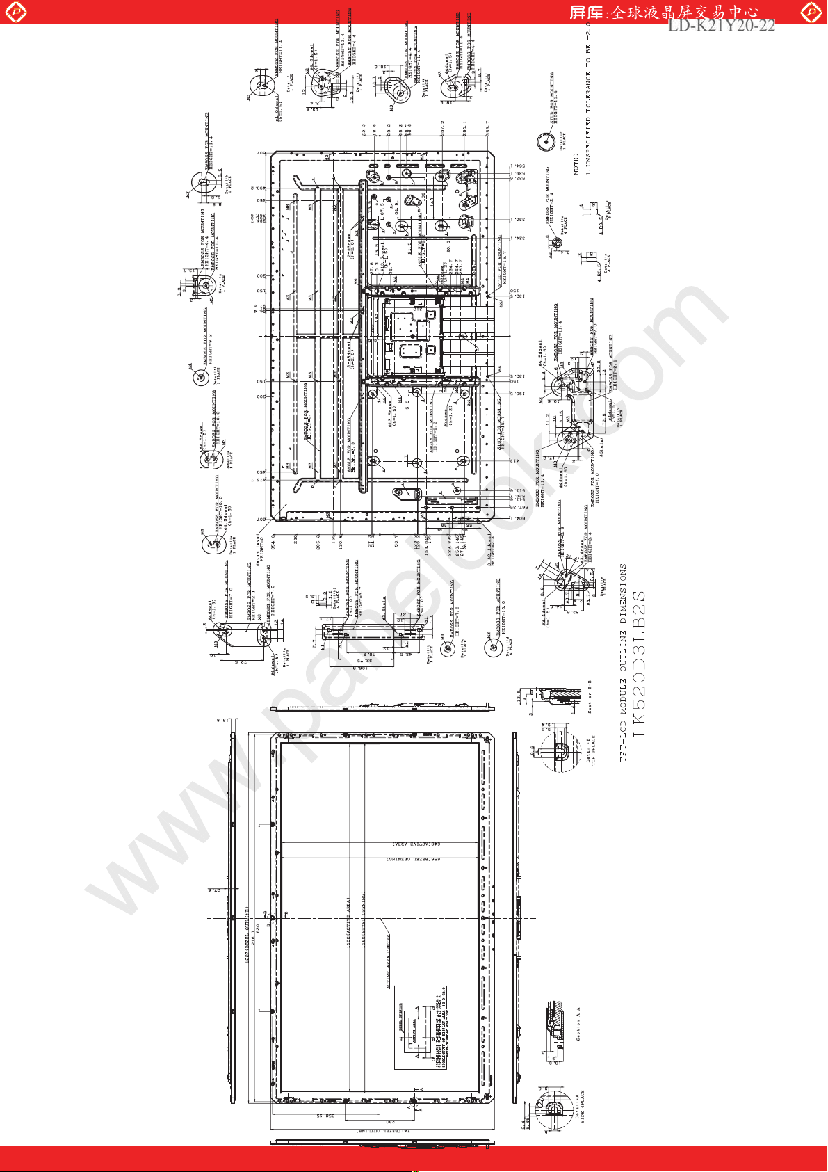
3. Mechanical Specifications
Parameter Specifications Unit
Display size
Active area 1152.0(H) × 648.0 (V) mm
Pixel Format
Pixel pitch 0.600 (H) × 0.600 (V) mm
Pixel configuration R, G, B vertical stripe
Display mode Normally black
Unit Outline Dimensions [Note] 1227 (W) × 741 (H) × 27.6 (D) mm
Mass 14.7 kg
Surface treatment
[Note] Outline dimensions are shown in Fig.17 (excluding protruding portion)
132.174 (Diagonal) cm
52.0 (Diagonal) inch
1920(H) × 1080(V)
(1pixel = R + G + B dot)
Clear LR(Low Reflection coating)
Hard coating: 3H
pixel
One step solution for LCD / PDP / OLED panel application: Datasheet, inventory and accessory!
www.panelook.com
Page 3
Global LCD Panel Exchange Center
4. Input Terminals
4.1. TFT panel driving
CN1 (Interface signals and +12V DC power supply) (Shown in Fig.1)
Using connector : FI-RNE51SZ-HF (Japan Aviation Electronics Ind., Ltd.)
Mating connector : FI-RE51HL, FI-RE51CL (Japan Aviation Electronics Ind., Ltd.)
Mating LVDS transmitter : THC63LVD1023 or equivalent device
Pin No. Symbol Function Remark
1
2
3
4
5
6
7
8
9
10
11 AIN0+ Aport (+)LVDS CH0 differential data input
12
13
14
15
16
17
18
19
20
21
22
23
24
25
26
27
28
29
30
31
32
33
34
35
36
37
38
39
40
41
42
43
44
45
VCC +12V Power Supply
VCC +12V Power Supply
VCC +12V Power Supply
VCC +12V Power Supply
VCC +12V Power Supply
Open
GND
GND
GND
AIN0-
AIN1- Aport (-)LVDS CH1 differential data input
AIN1+ Aport (+)LVDS CH1 differential data input
AIN2- Aport (-)LVDS CH2 differential data input
AIN2+ Aport (+)LVDS CH2 differential data input
GND
ACK- Aport LVDS Clock signal(-)
ACK+ Aport LVDS Clock signal(+)
GND
AIN3- Aport (-)LVDS CH3 differential data input
AIN3+ Aport (+)LVDS CH3 differential data input
AIN4- Aport (-)LVDS CH4 differential data input
AIN4+ Aport (+)LVDS CH4 differential data input
GND
BIN0- Bport (-)LVDS CH0 differential data input
BIN0+ Bport (+)LVDS CH0 differential data input
BIN1- Bport (-)LVDS CH1 differential data input
BIN1+ Bport (+)LVDS CH1 differential data input
BIN2- Bport (-)LVDS CH2 differential data input
BIN2+ Bport (+)LVDS CH2 differential data input
GND
BCK- Bport LVDS Clock signal(-)
BCK+ Bport LVDS Clock signal(+)
GND
BIN3- Bport (-)LVDS CH3 differential data input
BIN3+ Bport (+)LVDS CH3 differential data input
BIN4- Bport (-)LVDS CH4 differential data input
BIN4+ Bport (+)LVDS CH4 differential data input
GND
I2C_SCL I2C CLK
I2C_SDA I2C Data
Open
B-INT
PANEL_SEL
FRC_PWR_CTRL
Aport (-)LVDS CH0 differential data input
Open
I2C bus enable(H:enable, L:disable) [Note 1]
(PANEL Sel Signal) [Note 2]
Power on sequence(DC/DC On Signal)
www.panelook.com
LD- K21Y20-2
Open
Pull down : (GND)
Pull down : (GND)
One step solution for LCD / PDP / OLED panel application: Datasheet, inventory and accessory!
www.panelook.com
Page 4
Global LCD Panel Exchange Center
46
47
48
49
50
51
[Note] GND of a liquid crystal panel drive part has connected with a module chassis.
CN2 (+12V DC power supply)
Using connector : BM04B-PASS (J.S.T.Mfg Co., Ltd.)
Mating connector : (PAP-04V-S) (J.S.T.Mfg Co., Ltd.)
Pin No. Symbol Function Remark
1
2
3
4
SA_MODE
PANEL_ON
FRC_RST FRC IC RESET Pull down : (GND)
Open
TCON_RDY TCON ready signal (H:OK, L:NG)
Open
VCC +12V Power Supply
VCC +12V Power Supply
GND
GND
SA Mode Sel Signal
(L:Set mode, H:Stand alone(SA) mode)
Power on sequence
www.panelook.com
LD- K21Y20-3
Pull up +3.3V
Pull down : (GND)
Open
Open
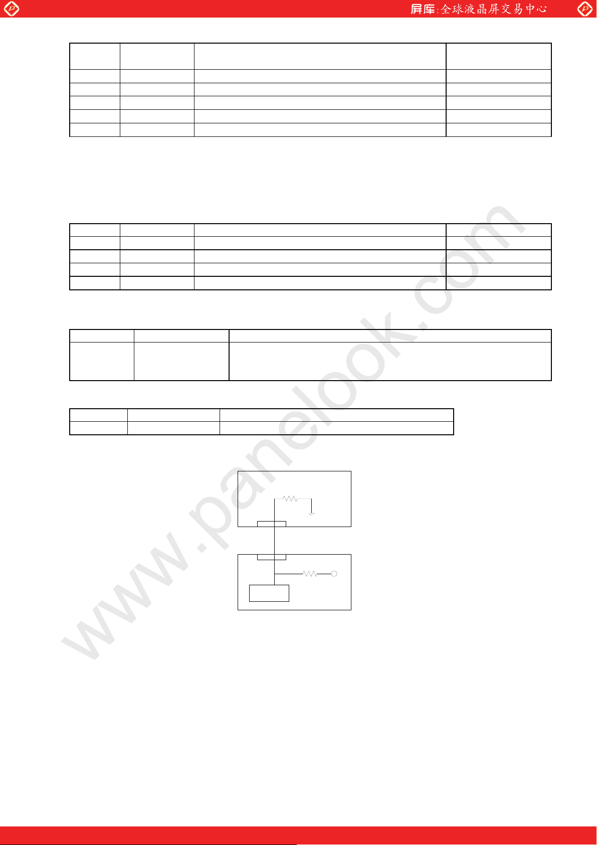
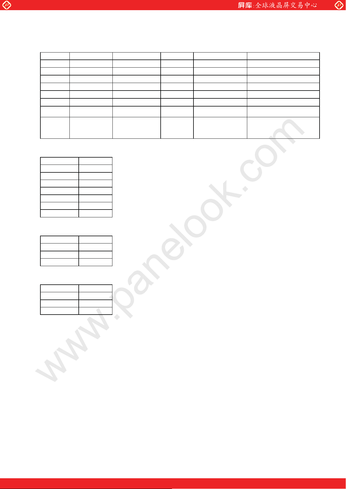
[Note 1] B_INT
Pin No. Symbol Function
43
[Note 2] PANEL_SEL
R1 Panel type Address
Open Standard Slave address and Power sequence are standard.
B_INT Select I2C Bus
0: FRC is I2C master. (EEPROM access mode )
1: FRC is I2C slave. (μ com mode(SA_MODE = ‘1’))
㪩㪈
㪫㪺㫆㫅㩷㪹㫆㪸㫉㪻
㪋㪎㫂
com
㱘
㪪㪼㫋㩷㪹㫆㪸㫉㪻
Fig.1 Block diagram of PANEL_SEL
One step solution for LCD / PDP / OLED panel application: Datasheet, inventory and accessory!
www.panelook.com
Page 5
Global LCD Panel Exchange Center
4.2. LVDS Data order
LVDS Mapping
Data [JEIDA]
TA0 R4
TA1 R5
TA2 R6
TA3 R7
TA4 R8
TA5 R9
TA6 G4
TB0 G5
TB1 G6
TB2 G7
TB3 G8
TB4 G9
TB5 B4
TB6 B5
TC0 B6
TC1 B7
TC2 B8
TC3 B9
TC4 HSYNC
TC5 VSYNC
TC6 DE (*)
TD0 R2
TD1 R3
TD2 G2
TD3 G3
TD4 B2
TD5 B3
TD6 N/A
TE0 R0
TE1 R1
TE2 G0
TE3 G1
TE4 B0
TE5 B1
TE6 N/A
NA:Not Available
(*)Since the display position is prescribed by the rise of DE(Display Enable) signal, please do not fix DE
signal during operation at ”High”.
www.panelook.com
LD- K21Y20-4
One step solution for LCD / PDP / OLED panel application: Datasheet, inventory and accessory!
www.panelook.com
Page 6
Global LCD Panel Exchange Center
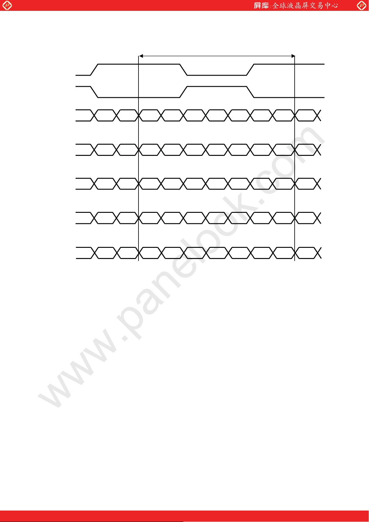
4.3. LVDS Mapping
ACK+,BCK+
ACK
– ,BCK–
AIN0+,BIN0+
AIN0
–,BIN0–
www.panelook.com
LD- K21Y20-5
1 cycle
G4 R9 R8 R7 R6 R5 R4 R4R5 G4
AIN1+,BIN1+
AIN1
–,BIN1–
AIN2+,BIN2+
AIN2
–,BIN2–
AIN3+,BIN3+
–,BIN3–
AIN3
AIN4+,BIN4+
–,BIN4–
AIN4
B5 B4 G9 G8 G7 G6 G5 G5G6 B5
DE
Vsync Hsync
B3 B2 G3 G2 R3 R2 R2R3 NANA
B1 B0 G1 G0 R1 R0 R0R1 NANA
B9 B8 B7 B6 B6B7
DE: Display Enable, NA: Not Available (Fixed Low)
Fig.2 LVDS Mapping
DE
One step solution for LCD / PDP / OLED panel application: Datasheet, inventory and accessory!
www.panelook.com
Page 7
Global LCD Panel Exchange Center
4.4. Panel ID data map
The slave address of EEPROM(24C02) is AA.
No. Item Spec(Ex.) Address Data Remark
1
2
3
4
5
6
7
8
[Note 1] Vender code
Vender code Data
SHARP
Vender code SHARP 00 03 Select Note1) *Sony use.
Screen size 52” 01 34
H-Resolution 1920 02,03 07,80
V-Resolution 1080 04,05 04,38
V-Frequency 200/240Hz 06 02 Select Note2)
Data format
Revision code
Part Number
-
-
-
-
-
-
00
01
02
03
04
05
06
www.panelook.com
10bit 07 02
001
LK520D3LB2S
FA〜FF
E0〜EF
30,30,31,00,00,00
4C,4B,35,32,30,44,
33,4C,42,32,53,00,
00,00,00,00
HEX data
HEX data
HEX data
Select Note3)
ASCII Note4)
ASCII Note4)
LD- K21Y20-6
*Sony use.
*Sony use.
[Note 2] V-Frequency
V-Frequency Data
50/60Hz
100/120Hz
200/240Hz
[Note 3] Data format
Data format Data
6bit
8bit
10bit
[Note 4] An empty address inputs “00”.
00
01
02
00
01
02
One step solution for LCD / PDP / OLED panel application: Datasheet, inventory and accessory!
www.panelook.com
Page 8
Global LCD Panel Exchange Center
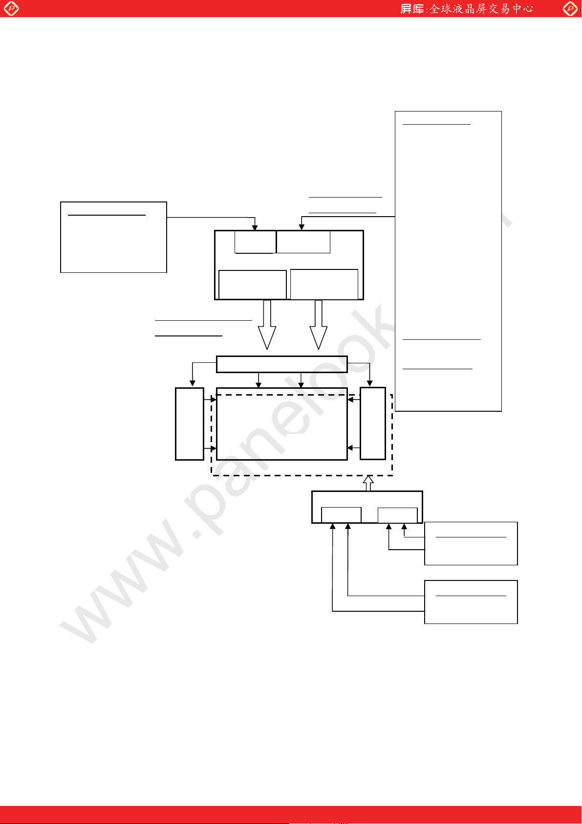
㪠㪥㪧㪬㪫㩷㪪㪠㪞㪥㪘㪣㪪㩷㩷㩷
㪦㪬㪫㪧㪬㪫㩷㪪㪠㪞㪥㪘㪣㪪
㩷
㪧㪦㪮㪜㪩㩷㪪㪬㪧㪧㪣㪰㩷
㩷
㩷
㩷
㩷
㪣㪚㪛㩷㪧㪘㪥㪜㪣㩷
㪈㪐㪉㪇㬍㪊㩿㪩㪞㪙㪀㬍㪈㪇㪏㪇㩷
㪞㪘㪫㪜㩷㪛㪩㪠㪭㪜㪩㩷
㪞㪘㪫㪜㩷㪛㪩㪠㪭㪜㪩㩷
㪚㪦㪥㪫㪩㪦㪣㩷㪧㪮㪙㩷
㪾
㪣㪜㪛㩷㪧㪮㪙㩷
㪧㪦㪮㪜㪩㩷㪪㪬㪧㪧㪣㪰㩷
㩿
㪀
㪪㪦㪬㪩㪚㪜 㪛㪩㪠㪭㪜㪩
Single Frame
-Rate Signal
Quadruple Frame
-Rate Signal
㪧㪦㪮㪜㪩㩷㪪㪬㪧㪧㪣㪰㩷
㩿
㪀
4.5. Interface block diagram
POWER SUPPLY
+12V DC
㩷
www.panelook.com
㩷
㪚㪥㪉㩷
㩷
㪚㫆㫅㫋㫉㫆㫃㩷
㫅㪸㫃㫊
㪪㫀
㪚㪥㪈㩷
㪧㫆㫎㪼㫉㩷㪪㫌㫇㫇㫃㫐
㪚㫀㫉㪺㫌㫀㫋㩷
LD- K21Y20-7
㪘㪠㪥㪇㪄㩷㪘㪠㪥㪇㪂㩷
㪘㪠㪥㪈㪄㩷㪘㪠㪥㪈㪂㩷
㪘㪠㪥㪉㪄㩷㪘㪠㪥㪉㪂㩷
㪘㪠㪥㪊㪄㩷㪘㪠㪥㪊㪂㩷
㪘㪠㪥㪋㪄㩷㪘㪠㪥㪋㪂㩷
㪘㪚㪢㪄㩷㪘㪚㪢㪂㩷
㪙㪠㪥㪇㪄㩷㪙㪠㪥㪇㪂㩷
㪙㪠㪥㪈㪄㩷㪙㪠㪥㪈㪂㩷
㪙㪠㪥㪉㪄㩷㪙㪠㪥㪉㪂㩷
㪙㪠㪥㪊㪄㩷㪙㪠㪥㪊㪂㩷
㪙㪠㪥㪋㪄㩷㪙㪠㪥㪋㪂㩷
㪙㪚㪢㪄㩷㪙㪚㪢㪂㩷
㪪㪚㪣㩷
㪪㪛㪘㩷
㪙㪶㪠㪥㪫㩷
㪧㪘㪥㪜㪣㪶㪪㪜㪣㩷
㪝㪩㪚㪶㪧㪮㪩㪶㪚㪫㪩㪣㩷
㪪㪘㪶㪤㪦㪛㪜㩷
㪧㪘㪥㪜㪣㪶㪦㪥㩷
㪝㪩㪚㪶㪩㪪㪫㩷
㩷
㪫㪚㪦㪥㪶㪩㪛㪰㩷
㩷
㩷 㩷 㪂㪈㪉㪭㩷㪛㪚㩷
㩷㩷
㪚㪥㪈㪇㪊
BACK LIGHT (LED276 package)
㪚㪥㪈㪇㪋
㪈㪉㪇㫄㪘㩷㫏㩷㪉㪣㫀㫅㪼㩷
㪄㪉㪊㪇㪭㩷‒㪛㪚
㪈㪉㪇㫄㪘㩷㫏㩷㪉㪣㫀㫅㪼㩷
㪂㪉㪊㪇㪭㩷‒㪛㪚
Fig.3 Interface block diagram
One step solution for LCD / PDP / OLED panel application: Datasheet, inventory and accessory!
www.panelook.com
Page 9
Global LCD Panel Exchange Center
4.6. Backlight driving
CN103 (+120mA DC power supply)
Using connector: 51103-0400 (Molex)
Mating connector: XAP-04V-1 (JST)
Pin No. Symbol Function Remark
1 I
2 I
+LED1
+LED2
3 Reserved -
4 Reserved
CN104 (-120mA DC power supply)
Using connector: 51103-0500 (Molex)
Mating connector: XAP-05V-1 (JST)
Pin No. Symbol Function Remark
1
2
3
I
-LED1
I
-LED2
Reserved
4 Reserved -
5 Reserved -
www.panelook.com
+120mA
-120mA -230V
-
+230V
LD- K21Y20-8
4.7. The back light system characteristics
The back light system is edge light type with 276 segment. (LS:4, LS:69packages)
The characteristics of the LED are shown in the following table. The value mentioned below is at the case of one
LED.
Item Symbol Min. Typ. Max. Unit Remarks
Life time TLED - 50000 - Hour [Note]
[Note] LED life time is defined as the time when brightness becomes 50% of the original value in the
continuous operation under the T
= 25qC
a
5. Absolute Maximum Ratings
Parameter Symbol Condition Ratings Unit Remark
Input voltage
(for Control and FRC)
12V supply voltage
(for Control)
supply current
(for LED driver)
supply voltage
(for LED driver)
I
V
VCC
I
LED
V
LED
Ta = 25 qC
Ta = 25 qC
Tj = 25 qC
Tj = 25 qC
-0.3 ~ 3.6 V [Note 1]
0 ~ + 14 V
150 mA
-242 ~ +242 V
Storage temperature T
Operation temperature
(Ambient)
- -25 ~ +60
stg
- -0 ~ +50
T
opa
qC
qC
[Note 1] SCL, SDA, B_INT, PANEL_SEL, FRC_PWR_CTRL, SA_MODE, PANEL_ON, FRC_RST
One step solution for LCD / PDP / OLED panel application: Datasheet, inventory and accessory!
www.panelook.com
Page 10

Global LCD Panel Exchange Center
T
)
6. Electrical Characteristics
6.1. Control circuit driving Ta=25 qC
Parameter Symbol Min. Typ. Max. Uniit Remark
Supply voltage Vcc 11 12 13 V [Note 1]
+12V supply
voltage
Permissible input ripple voltage VRP - - 100 mVP-P Vcc = +12.0V
threshold voltage
Input High voltage VIH 2.3 - 3.6 V
Input leak current(Low) IIL 400 μA VI=0V
Input leak current(High) IIH 100 μA VI=3.3V
Input Differential voltage |VID| 100 - - mV
common mode voltage
[Note]VCM: Common mode voltage of LVDS driver.
[Note 1]
Current dissipation Icc - 2.1 4.0 A [Note 2]
Inrush current
High VTH - - 100 mV Differential input
Low V
Input Low voltage VIL 0 - 1.0 V
Terminal resistor RT - 100 -
Differential input
www.panelook.com
LD- K21Y20-9
I
1 - 9.4 - A
RUSH
2 - 3.2 - A t1>5ms
I
RUSH
TL -100 - - mV
:
|VID|/2 1.2
V
CM
|V
2.4-
ID
|/2
V
t1=500μs
[Note 4]
V
CM = +1.2V
[Note 6]
[Note 5]
Differential
input
[Note 3]
Power3
Typ x 90%
Panel5/1 2V
T_BINT
/Write Protect
EDID Read
PANEL_I2C
FRC_PWR_CTR
LVDS-Rx
X_FRC_RESET T8b
TCON_RDY
Typ x 10%
T1
3b
T5
T6a
T11a
T2a
T3a
T2b
T6b
T8c
T7b
T11c
T11b
T18
T22
T19
90%
10%
T23
O/S_LUT
Back Light(BL_ON
T16a
T14
T16 b
T15
T15
T17
Fig.4 Timing chart of sequence
One step solution for LCD / PDP / OLED panel application: Datasheet, inventory and accessory!
www.panelook.com
Page 11

Global LCD Panel Exchange Center
Min Max Min Max Min Max Min Max Unit
T1 0.47 10 T7b 60 T16b 500 T23 0
T2b 60 T8b 10 T17 100
T3b 0 200 T8c 10 T18 0 10
T5 10 T14 0 T19 0 45
T6b 50 T15 0.1 T22 0 T22
[Note]About the relation between data input and back light lighting, please base on the above-mentioned input
sequence. When back light is switched on before panel operation or after a panel operation stop, it may not display
normally. But this phenomenon is not based on change of an incoming signal, and does not give damage to a liquid
crystal display.
[Note 2] Typical current situation: 1024 gray-bar patterns. (Vcc = +12.0V)
The explanation of RGB gray scale is seen in section 8.
www.panelook.com
LD- K21Y20-10
msec
RGB
GS0
RGB
GS1
RGB
GS2
....
GS1022
RGB
RGB
GS1023
CK=74.25MHz
Th=14.1μs
Max.current situation: 2H hatching pattern. (Vcc = +12.0V)
CK=74.25MHz
GS0
Th=14.8μs
GS0
GS1023
Zoom
GS1023
Vcc=+12.0V
Magnify
GS1023
GS0
GS0
GS1023
GS1023
GS0
GS0
GS1023
Vcc=+12.0V
Fig.5 Typical/Worst Display pattern
One step solution for LCD / PDP / OLED panel application: Datasheet, inventory and accessory!
www.panelook.com
Page 12

Global LCD Panel Exchange Center
[Note 3]
*CK-,*IN-
www.panelook.com
LD- K21Y20-11
|VID|
*CK+,*IN+
[Note 4]
|VID|
VCM
GND
Fig.6 mini-LVDS Amplitude voltage
500us
VCC12V
9.4A
Fig.7 Inrush Current
[Note 5] I2C_SCL,I2C_SDA,B_INT,PANEL_SEL,FRC_PWR_CTRL
SA_MODE,PANEL_ON,FRC_RST,TCON_RDY
Inrush
One step solution for LCD / PDP / OLED panel application: Datasheet, inventory and accessory!
www.panelook.com
Page 13

Global LCD Panel Exchange Center
6.2. LED driving for back light
The back light system is edge light type with LEDs .
Parameter Symbol Min. Typ. Max. Unit Remark
Operating Voltage Vop ±216 ±230 ±242 V @240mA/module
Operating Current I
7. Timing characteristics of input signals
7.1. Timing characteristics
Timing diagrams of input signal are shown in Fig.3.
FRC Input Timing
60Hz 50Hz 24×2
H_Total dot 2184
H_Active dot 1920
H_FP①
H_FP②
HS_Width dot 32 3232 32
H_BP①
H_BP②
H_freq kHz
V_Total line 1124
V_Active line 1080
V_FP line 24 3444 247
VS_Width line 4
V_BP line 16 1616 16
V_freq Hz 59.46
PanelCLK MHz 73.51
Symbol
www.panelook.com
- 120 - mA 1 pair Current
op
- 240 - mA Total Current(2 pair)
min.
dot 32
dot 136
dot 200
dot 96
typ.
2184
1920
136
200
67.995 67.995 67.995
1134
1080
59.96
74.25
32
96
4
max. min.
2184 2184
1920 1920
32 32
136 136
200 200
96 96
1144 1347
1080 1080
4 4
60.46 49.50
74.99 73.51
typ.
2184
1920
32
136
32
200
96
1360
1080
260
4
16
49.97
74.25
LD- K21Y20-12
max. min.
2184 2184
1920 1920
32 32
136 136
32 32
200 200
96 96
1374 1402
1080 1080
274 302
4 4
16 16
50.50 47.52
74.99 73.51
typ.
2184
1920
32
136
32
200
96
1416
1080
316
4
16
48.02
74.25
max.
2184
1920
32
136
32
200
96
1430
1080
330
4
16
48.52
74.99
[Note]-When vertical period is very long, flicker and etc. may occur.
-Please turn off the module after it shows the black screen.
-Please make sure that length of vertical period should become of an integral multiple of horizontal
length of period. Otherwise, the screen may not display properly.
-As for your final setting of driving timing, we will conduct operation check test at our side, please
inform your final setting.
-It is defined under the input signal condition with SS (60 kHz/±2%).
Htotal ; 2184±1 lines
One step solution for LCD / PDP / OLED panel application: Datasheet, inventory and accessory!
www.panelook.com
Page 14

Global LCD Panel Exchange Center
DE
www.panelook.com
LD- K21Y20-13
TH
THd
Aport DATA
1
(R,G,B)
Bport DATA
1920 1920
2
(R,G,B)
Tc
DE
TV
Fig.8 LVDS input timing chart
7.2. Input data signal and display position on the screen
31919 1919
4
1 2 1080
1079
TVd
R1 G1 B1 R2 G2 B2
(1、1) (1,2)
1・1 1・2 1・3
2・1 2・2
3・1
1080・1
R1 G1 B1 R2 G2 B2
(1、3) (1,4)
Source Bora d side
1・4
R G B
Display position of Data (V,H)
1・1920
1080・1920
Fig.9 Input data signal and display position on the screen
One step solution for LCD / PDP / OLED panel application: Datasheet, inventory and accessory!
www.panelook.com
Page 15

Global LCD Panel Exchange Center
8. Input Signal, Basic Display Colors and Gray Scale of Each Color
www.panelook.com
LD- K21Y20-14
Colors &
Gray scale
Black – 0 0 0 0 0 0 0 0 0 0 0 0 0 0 0 0 0 0 0 0 0 0 0 0 0 0 0 0 0 0
Blue – 0 0 0 0 0 0 0 0 0 0 0 0 0 0 0 0 0 0 0 0 1 1 1 1 1 1 1 1 1 1
Green – 0 0 0 0 0 0 0 0 0 0 1 1 1 1 1 1 1 1 1 1 0 0 0 0 0 0 0 0 0 0
Cyan – 0 0 0 0 0 0 0 0 0 0 1 1 1 1 1 1 1 1 1 1 1 1 1 1 1 1 1 1 1 1
Red – 1 1 1 1 1 1 1 1 1 1 0 0 0 0 0 0 0 0 0 0 0 0 0 0 0 0 0 0 0 0
Basic Color
Magenta – 1 1 1 1 1 1 1 1 1 1 0 0 0 0 0 0 0 0 0 0 1 1 1 1 1 1 1 1 1 1
Yellow – 1 1 1 1 1 1 1 1 1 1 1 1 1 1 1 1 1 1 1 1 0 0 0 0 0 0 0 0 0 0
White – 1 1 1 1 1 1 1 1 1 1 1 1 1 1 1 1 1 1 1 1 1 1 1 1 1 1 1 1 1 1
Black GS0 0 0 0 0 0 0 0 0 0 0 0 0 0 0 0 0 0 0 0 0 0 0 0 0 0 0 0 0 0 0
× GS1 1 0 0 0 0 0 0 0 0 0 0 0 0 0 0 0 0 0 0 0 0 0 0 0 0 0 0 0 0 0
Darker GS2 0 1 0 0 0 0 0 0 0 0 0 0 0 0 0 0 0 0 0 0 0 0 0 0 0 0 0 0 0 0
×
Ø
Brighter GS1021 1 0 1 1 1 1 1 1 1 1 0 0 0 0 0 0 0 0 0 0 0 0 0 0 0 0 0 0 0 0
R0 R1 R2 R3 R4 R5 R6 R7 R8 R9 G0 G1 G2 G3 G4 G5 G6 G7 G8 G9 B0 B1 B2 B3 B4 B5 B6 B7 B8 B9
Gray
Scale
pp p p
pp p p
Gray Scale of Red
Ø GS1022 0 1 1 1 1 1 1 1 1 1 0 0 0 0 0 0 0 0 0 0 0 0 0 0 0 0 0 0 0 0
Data signal
Red GS1023 1 1 1 1 1 1 1 1 1 1 0 0 0 0 0 0 0 0 0 0 0 0 0 0 0 0 0 0 0 0
Black GS0 0 0 0 0 0 0 0 0 0 0 0 0 0 0 0 0 0 0 0 0 0 0 0 0 0 0 0 0 0 0
× GS1 0 0 0 0 0 0 0 0 0 0 1 0 0 0 0 0 0 0 0 0 0 0 0 0 0 0 0 0 0 0
Darker GS2 0 0 0 0 0 0 0 0 0 0 0 1 0 0 0 0 0 0 0 0 0 0 0 0 0 0 0 0 0 0
×
Ø
Brighter GS1021 0 0 0 0 0 0 0 0 0 0 1 0 1 1 1 1 1 1 1 1 0 0 0 0 0 0 0 0 0 0
Gray Scale of Green
Ø GS1022 0 0 0 0 0 0 0 0 0 0 0 1 1 1 1 1 1 1 1 1 0 0 0 0 0 0 0 0 0 0
Green GS1023 0 0 0 0 0 0 0 0 0 0 1 1 1 1 1 1 1 1 1 1 0 0 0 0 0 0 0 0 0 0
Black GS0 0 0 0 0 0 0 0 0 0 0 0 0 0 0 0 0 0 0 0 0 0 0 0 0 0 0 0 0 0 0
pp p p
pp p p
× GS1 0 0 0 0 0 0 0 0 0 0 0 0 0 0 0 0 0 0 0 0 1 0 0 0 0 0 0 0 0 0
Darker GS2 0 0 0 0 0 0 0 0 0 0 0 0 0 0 0 0 0 0 0 0 0 1 0 0 0 0 0 0 0 0
Ø
Ø
Brighter GS1021 0 0 0 0 0 0 0 0 0 0 0 0 0 0 0 0 0 0 0 0 1 0 1 1 1 1 1 1 1 1
Gray Scale of Blue
Ø GS1022 0 0 0 0 0 0 0 0 0 0 0 0 0 0 0 0 0 0 0 0 0 1 1 1 1 1 1 1 1 1
Blue GS1023 0 0 0 0 0 0 0 0 0 0 0 0 0 0 0 0 0 0 0 0 1 1 1 1 1 1 1 1 1 1
pp p p
pp p p
0: Low level voltage, 1: High level voltage.
Each basic color can be displayed in 1021 gray scales from 10 bits data signals. According to the combination of
total 30 bits data signals, one billion-color display can be achieved on the screen.
One step solution for LCD / PDP / OLED panel application: Datasheet, inventory and accessory!
www.panelook.com
Page 16
Global LCD Panel Exchange Center
9. Optical characteristics
Ta=2 5°C, Vcc=12.0V, LED current=±120mA and PWM=100%, Timing: 240Hz(typ. value)
Parameter Symbol Condition Min. Typ. Max. Unit Remark
Viewing angle
range
Contrast ratio CRn - 5000 - - [Note2,4]
Horizontal
Vertical
θ
θ
θ
θ
21
22
11
12
www.panelook.com
70 88 - Deg.
CR ≥ 10
70 88 -
LD- K21Y20-15
[Note1,4]
Deg.
Response time
White
Red
Chromaticity
Green
Blue
Luminance White YL 370 460 - cd/m
Luminance
uniformity
Measurement condition: Set the value of LED current=±120mA and PWM=100% luminance of white.
*The measurement shall be executed 60 minutes after lighting at rating.
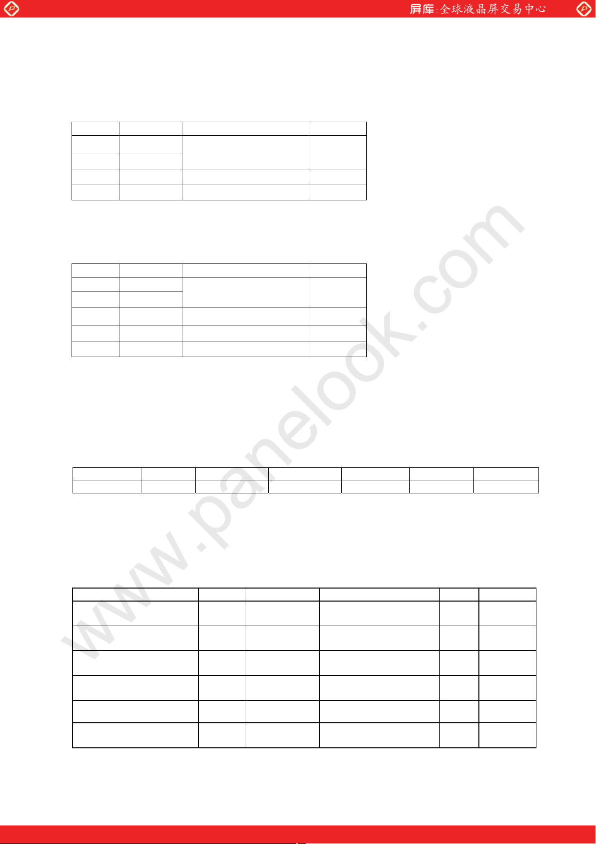
[Note] The optical characteristics are measured using the following equipment.
Detector㸦EZ-CONTRAST/ Photodiode㸧
Middle of the screen (θ㸻0°)
TFT-LCD Module
Fig.10-1 Measurement of Viewing angle range and
Response time.
White
Viewing angle range: EZ-CONTRAST
Response time: Photodiode
τ
δw
DRV
x
y
x
y
x
y
x
y
θ
= 0 deg.
- 4 8 msec [Note3,4,5]
0.250 0.280 0.310
0.255 0.285 0.315
0.642 0.647 0.652
0.339 0.344 0.349
0.298 0.303 0.308
0.647 0.652 0.657
0.151 0.156 0.161
0.046 0.051 0.056
- - 0.25 - [Note 6]
Detector (SR-3)
400mm
Field=1°
Middle of the screen (θ㸻0°)
TFT-LCD Module
Fig.10-2 Measurement of Contrast,
Luminance, and Chromaticity.
-
-
-
-
-
-
-
-
2
[Note4]
Fig.10 Optical measuringequipment
One step solution for LCD / PDP / OLED panel application: Datasheet, inventory and accessory!
www.panelook.com
Page 17

Global LCD Panel Exchange Center
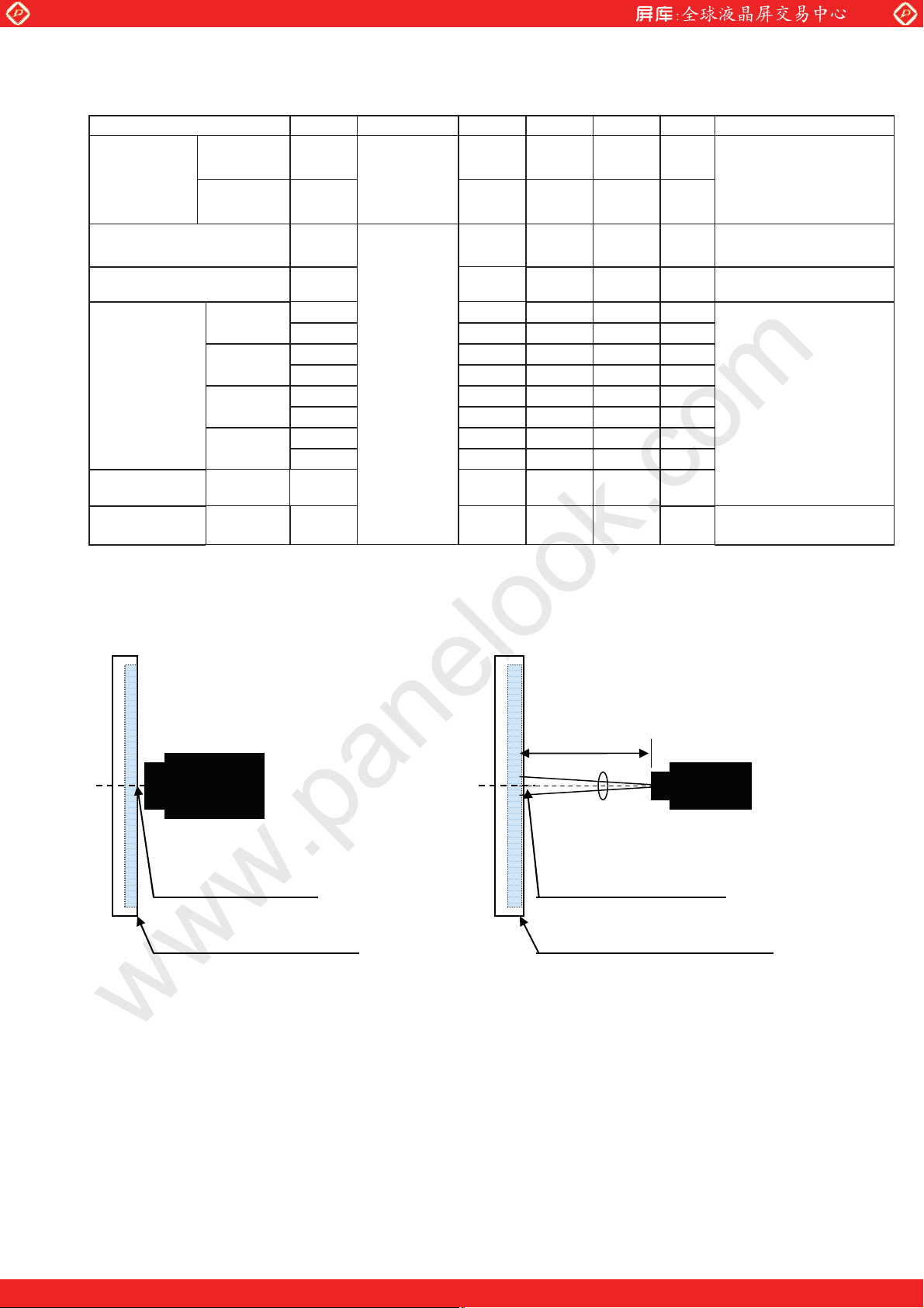
[Note 1] Definitions of viewing angle range :
T
22
T
12
[Note 2]Definition of contrast ratio :
The contrast ratio is defined as the following.
www.panelook.com
Normal line
T
11
T
21
6 o’clock direction
Fig.11 Optical measurement condition
LD- K21Y20-16
Luminance (brightness) with all pixels white
Contrast Ratio
=
Luminance (brightness) with all pixels black
[Note 3]Definition of response time
The response time (T
)) is defined as the following figure and shall be measured by switching the input
DRV
signal for “any level of gray (0%, 25%, 50%, 75% and 100%)” and “any level of gray (0%, 25%, 50%, 75%
and 100%)”.
0%
0%
25% 50% 75%
tr:0%-25%
tr:0%-50% tr:0%-75% tr:0%-100%
100%
25% td: 25%-0% tr: 25%-50% tr25%-75% tr: 25%-100%
50% td: 50%-0% td: 50%-25%
75% td: 75%-0% td: 75%-25% td: 75%-50%
tr: 50%-75
% tr: 50%-100%
tr: 75%-100
%
100% td: 100%-0% td: 100%-25% td: 100%-50% td:100%-75%
t*:x-y...response time from level of gray(x) to level of gray(y)
W
= 6(t*:x-y)/20
DRV
any level of gray
(bright)
any level of glay
(dark)
any level of gray
(bright)
100%
90%
Photodetector
10%
Output
0%
td:* tr:*
time
Fig.12 Definition of response time
[Note 4] This shall be measured at center of the screen.
[Note 5] This value is valid when O/S driving is used at typical input time value.
One step solution for LCD / PDP / OLED panel application: Datasheet, inventory and accessory!
www.panelook.com
Page 18
Global LCD Panel Exchange Center
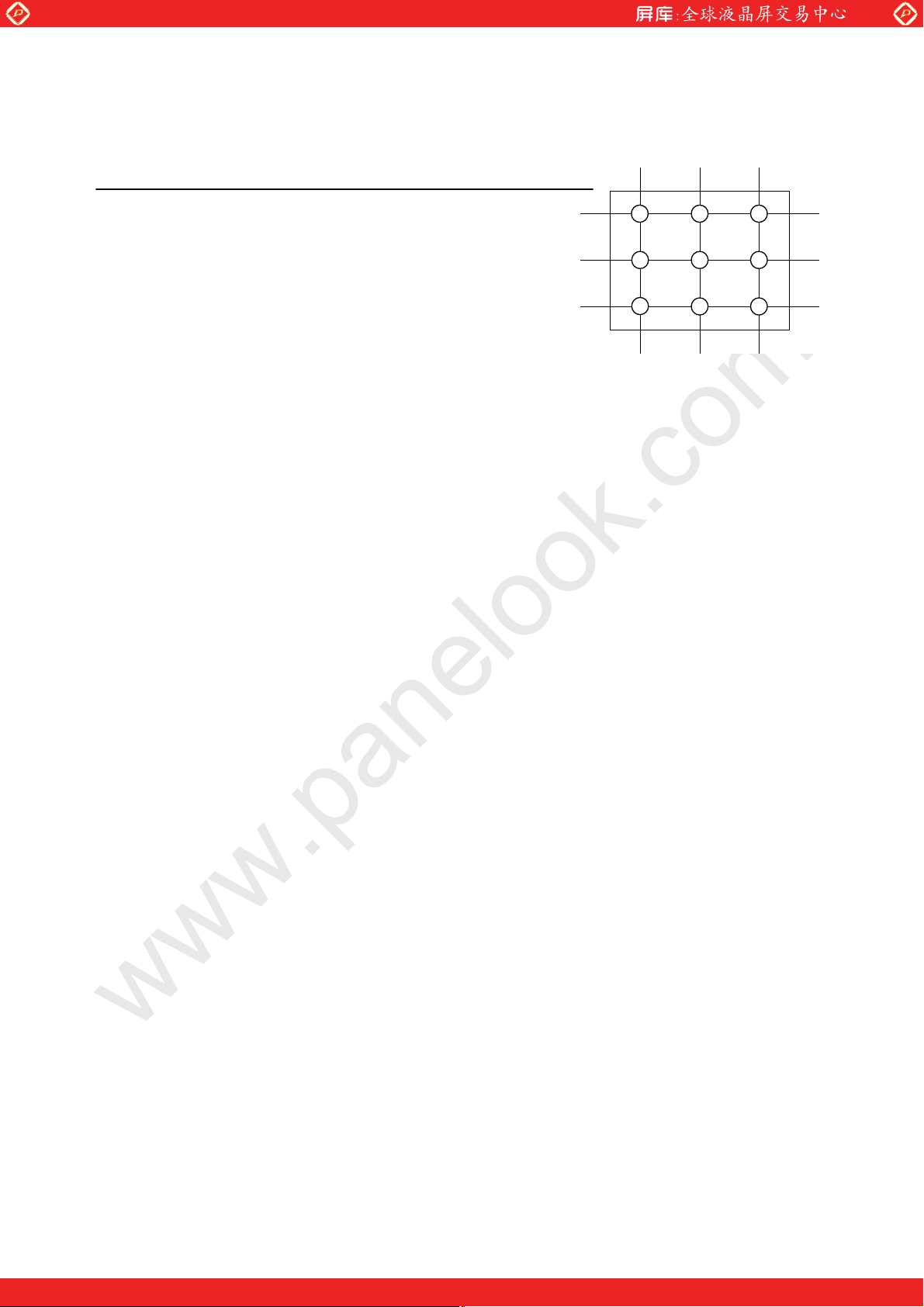
[Note 6] Definition of white uniformity ;
White uniformity is defined as the following with nine measurements. (AaI)
www.panelook.com
LD- K21Y20-17
|Maximum or Minimum luminance of nine points – Luminance of center point ”E” |
W=
G
Luminance of center point “E”
Fig.13 Definition of white uniformity
10. Handling Precautions of the module
a) Be sure to turn off the power supply when inserting or disconnecting the cable.
b) Voltage difference generated by this switching, 'V
supply is shared between the LED driver and its surrounding circuit. So, separate the power supply of the
LED driver circuit with the one of its surrounding circuit.
*Since LED driver board’s GND is not connected to the frame of the LCD module, please connect it with the
Customer’s GND of LED driver power supply.
c) Be sure to design the cabinet so that the module can be installed without any extra stress such as warp or
twist.
d) Since the front polarizer is easily damaged, pay attention not to scratch it.
e) Since long contact with water may cause discoloration or spots, wipe off water drop immediately.
f) When the panel surface is soiled, wipe it with absorbent cotton or other soft cloth.
g) Since the panel is made of glass, it may break or crack if dropped or bumped on hard surface. Handle with
care.
LED, may affect a sound output, etc. when the power
320 960 1600
A
B
C
D
E
F
G
H
pixel
180
540
I
900
pixel
h) Since CMOS LSI is used in this module, take care of static electricity and take the human earth into
consideration when handling.
i) The module has some printed circuit boards (PCBs) on the back side, take care to keep them form any stress
or pressure when handling or installing the module; otherwise some of electronic parts on the PCBs may be
damaged.
j) Observe all other precautionary requirements in handling components.
k) When some pressure is added onto the module from rear side constantly, it causes display non-uniformity
issue, functional defect, etc. So, please avoid such design.
l) When giving a touch to the panel at power on supply, it may cause some kinds of degradation. In that case,
once turn off the power supply, and turn on after several seconds again, and that is disappear.
m) When handling LCD modules and assembling them into cabinets, please be noted that long-term storage in
the environment of oxidization or deoxidization gas and the use of such materials as reagent, solvent,
adhesive, resin, etc. which generate these gasses, may cause corrosion and discoloration of the LCD
modules.
n) This LCD module is designed to prevent dust from entering into it. However, there would be a possibility to
have a bad effect on display performance in case of having dust inside of LCD module. Therefore,
please ensure to design your TV set to keep dust away around LCD module.
One step solution for LCD / PDP / OLED panel application: Datasheet, inventory and accessory!
www.panelook.com
Page 19
Global LCD Panel Exchange Center
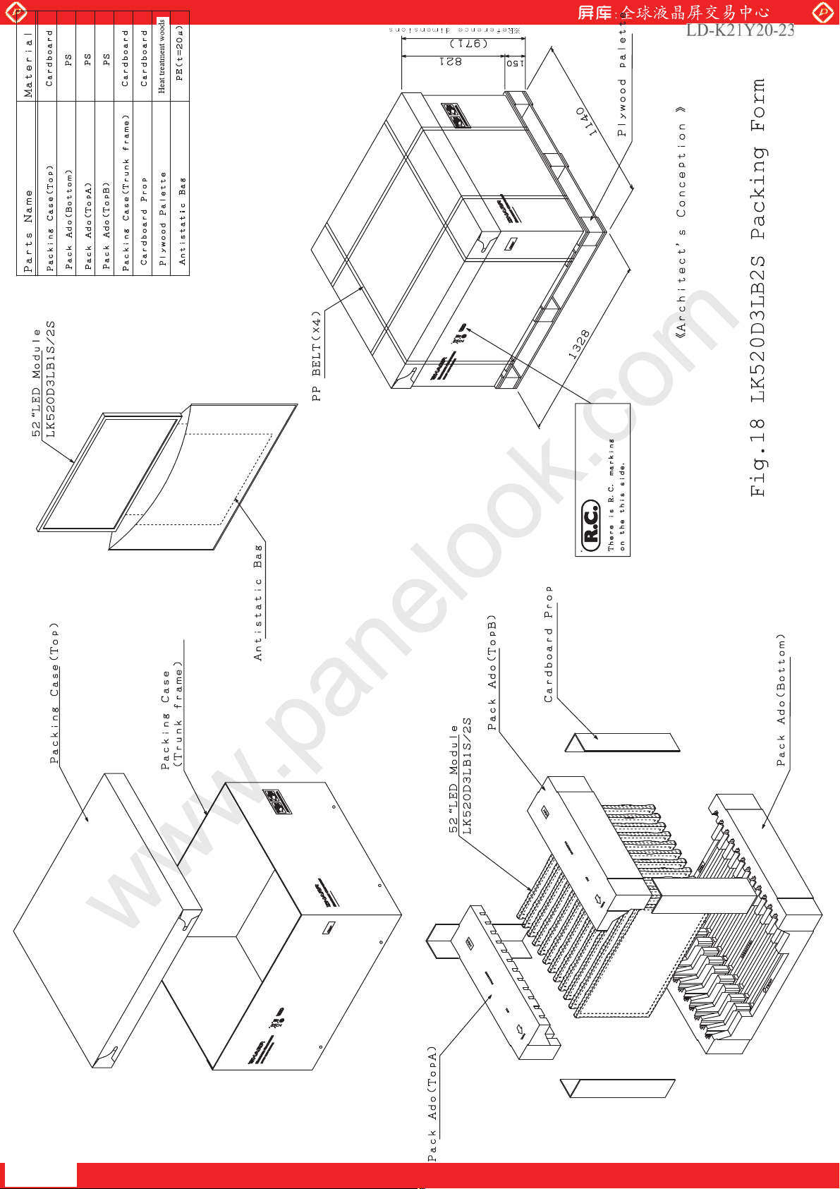
11. Packing form
a) Piling number of cartons : 4 maximum
b) Packing quantity in one carton : 12 pcs maximum
c) Carton size : 1140 mm (W) × 1328(D) × 971(H)
d) Total mass of one carton filled with full modules : 210kg maximum
[Note] Packing form are shown in Fig.18
12. Reliability test item
No. Test item Condition
1
2
3
4
5
6
7
8
[Result evaluation criteria]
Under the display quality test condition with normal operation state, there shall be no change, which may
affect practical display function.
High temperature storage test
Low temperature storage test
High temperature and high humidity
operation test
High temperature operation test
Low temperature operation test
Vibration test
(non-operation)
Shock test
(non-operation)
ESD
www.panelook.com
Ta = 60qC 240h
Ta = -25qC 240h
Ta = 40qC ; 95%RH 240h
(No condensation)
Ta = 50qC 240h
Ta = 0qC 240h
Frequency: 10~57Hz/Vibration width (one side): 0.075mm
: 57~500Hz/Acceleration: 9.8 m/s²
Sweep time: 11 minutes
Test period: 3 hours (1h for each direction of X, Y, Z)
Maximum acceleration: 294m/s
Pulse width: 11ms, sinusoidal half wave
Direction: +/-X, +/-Y, +/-Z, once for each direction.
* At the following conditions, it is a thing without incorrect
operation and destruction.
(1)Non-operation: Contact electric discharge r10kV
(2)Operation Contact electric discharge r8kV
Conditions: 150pF, 330ohm
LD- K21Y20-18
2
Non-contact electric discharge r20kV
Non-contact electric discharge r15kV
One step solution for LCD / PDP / OLED panel application: Datasheet, inventory and accessory!
www.panelook.com
Page 20
Global LCD Panel Exchange Center
A
A
A
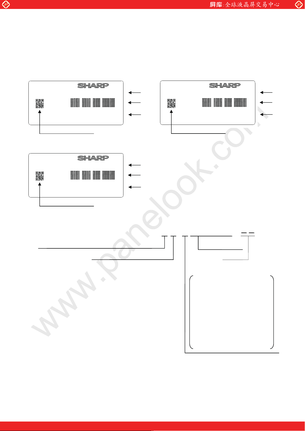
13. Others
1) Lot No. Label ;
The label that displays SHARP, product model (LK520D3LB2S), a product number is stuck on the back of the
module.
[LK520D3LB2SP, 2SK] NSEC PRODUCTION [LK520D3LB2SZ] SEMEX PRODUCTION
www.panelook.com
LD- K21Y20-19
䌌䌑䋳䋷䋰䌄䋳䌌䌚䋱䋴
LK520D3LB2S
9Z XXXXXX P (or K)
䋵䋹䇭䌘䌘䌘䌘䌘䌘
䌍䌁䌄䌅䇭䌉䌎䇭䌊䌁䌐䌁䌎
2D Barcode
[LK520D3LB2SY] SMPL PRODUCTION
䌌䌑䋳䋷䋰䌄䋳䌌䌚䋱䋴
LK520D3LB2S
䋵䋹䇭䌘䌘䌘䌘䌘䌘
9Z XXXXXX Y
䌍䌁䌄䌅䇭䌉䌎䇭䌊䌁䌐䌁䌎
2D Barcode
Model No.
Barcode
Lot No.
Model No.
Barcode
Lot No.
䌌䌑䋳䋷䋰䌄䋳䌌䌚䋱䋴
LK520D3LB2S
9Z XXXXXX Z
䋵䋹䇭䌘䌘䌘䌘䌘䌘
䌍䌁䌄䌅䇭䌉䌎䇭䌊䌁䌐䌁䌎
2D Barcode
How to express Lot No.
○
○
○
○○○
○
Model No.
Barcode
Lot No.
○
production year(the last figures of the Christian Era)
production month (1-9,X,Y,Z)
-
Fig.14 Lot number label description specification
Serial No.
Management No.
Identification Code
K:Kameyama Plant.
L:Kameyama Tec. Kameyama Fab.
J:Kameyama Tec. Yaita Fab.
S:SHM
N:NSEC
P:SMPL
G:SMM
X:SEMEX
or B:JABIL
One step solution for LCD / PDP / OLED panel application: Datasheet, inventory and accessory!
www.panelook.com
Page 21
Global LCD Panel Exchange Center
(
4S
)
(Q)
(
4S
)
(Q)
(
4S
)
(Q)
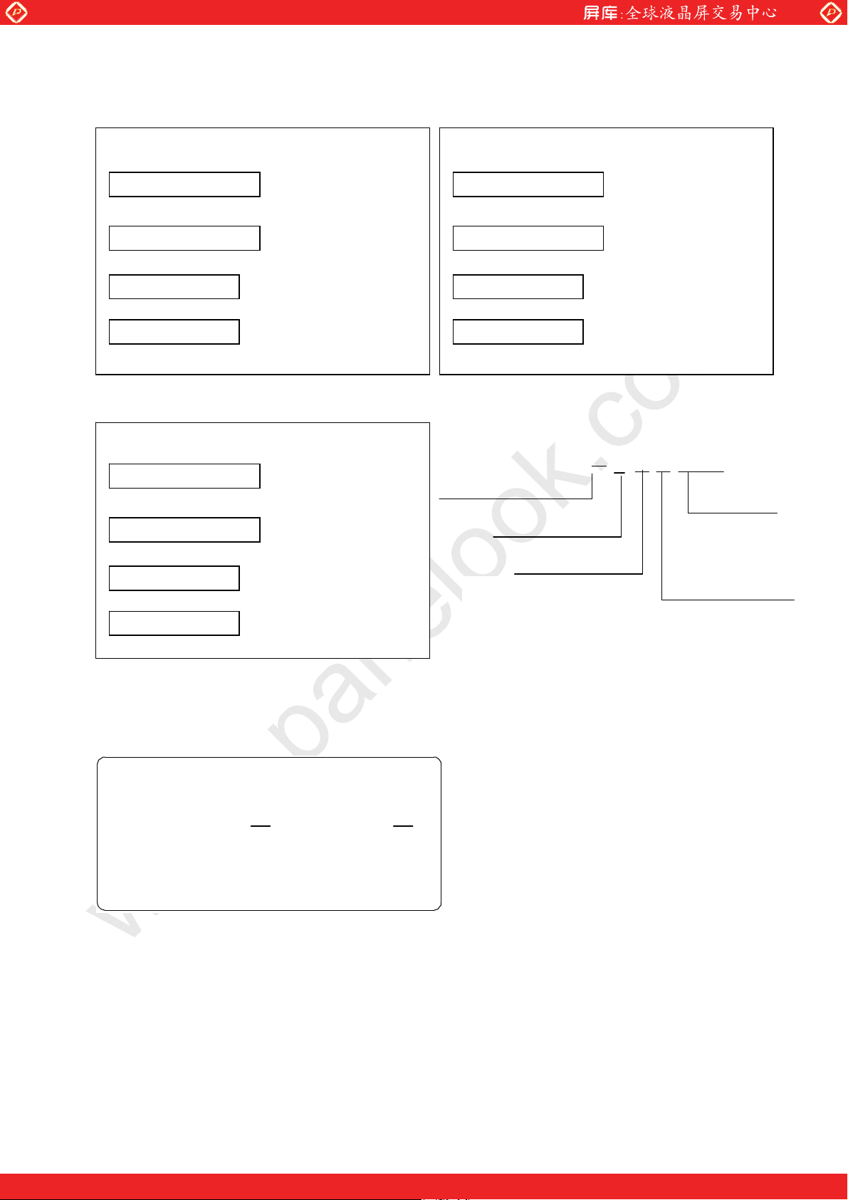
2) Packing Label
[LK520D3LB2SP,2SK] NSEC PRODUCTION [LK520D3LB2SZ] SEMEX PRODUCTION
www.panelook.com
LD- K21Y20-20
␠ౝຠ⇟㧦
㧽㨡㨍㨚㨠㨕㨠㨥㧦
Bar code
࡙ࠩຠ⇟
Bar code
シャープ物流用ラベルです。
[LK520D3LB2SY] SMPL PRODUCTION
␠ౝຠ⇟㧦
㧽㨡㨍㨚㨠㨕㨠㨥㧦
Bar code
࡙ࠩຠ⇟
Bar code
シャープ物流用ラベルです。
Bar code
Bar code
Bar code
(1T)20**.**.** * ***** (②)㧸㨛㨠㧺㧻㧚
Bar code
LK520D3LB3SP (K) (①)
12
pcs (③)
LK520D3LB2SY (①)
12
pcs (③)
/1&'.㧦
㧽㨡㨍㨚㨠㨕㨠㨥㧦
Bar code
࡙ࠩຠ⇟
Bar code
シャープ物流用ラベルです。
A production year(09-99)
Bar code
(1T)20**.**.** * ***** (②)㧸㨛㨠㧺㧻㧚(1T)20**.**.** * ***** (②)㧸㨛㨠㧺㧻㧚
Bar code
month (1-9, X,Y, Z)
① Management No
② Lot No. (Date)
③ Quantity
LK520D3LB3SZ (①)
How to express Lot No.
.**.** * *****
20**
Day (1-31)
pcs (③)
12
Box Serial No[Note1]
Identification Code
[Note 1] Box Serial Number is nine digits only the JABIL POLAND production, and besides, five digits.
Fig.15 Packing label description specification
3)Material Label
䌍䌁䌔䌅䌒䌉䌁䌌䇭䌉䌎䌆䌏䌒䌍䌁䌔䌉䌏䌎
䌒䌥䌦䌬䌥䌣䌴䌩䌶䌥䇭䌐䌯䌬䌡䌲䌩䌺䌥䌲䋺䋾䌐䌃䋬䌐䌅䌓䌔䋬䌁䌋䌕䌒䋭䌘䋬䌐䌃䋼
䌌䌥䌮䌳䇭䌆䌩䌬䌭䋺䋾䌐䌃䋼
䌄䌩䌦䌦䌵䌳䌥䌲䇭䌓䌨䌥䌥䌴䋺䋾䌐䌅䌔䋼
䌌䌩䌧䌨䌴䇭䌇䌵䌩䌤䌥䋺䋾䌐䌍䌍䌁䋼
䌒䌥䌦䌬䌥䌣䌴䌩䌶䌥䇭䌓䌨䌥䌥䌴䋺䋾䌐䌅䌔䋼
Fig.16 Material label description specification
4) Adjusting volume has been set optimally before shipment, so do not change any adjusted value.
If adjusted value is changed, the specification may not be satisfied.
5) Disassembling the module can cause permanent damage and should be strictly avoided.
6) Please be careful since image retention may occur when a fixed pattern is displayed for a long time.
7) The chemical compound, which causes the destruction of ozone layer, is not being used.
8) When any question or issue occurs, it shall be solved by mutual discussion.
9) This module is corresponded to RoHS.
One step solution for LCD / PDP / OLED panel application: Datasheet, inventory and accessory!
www.panelook.com
Page 22
Global LCD Panel Exchange Center
14. Carton storage condition
Temperature 0qC to 40qC
Humidity 95%RH or less
Reference condition : 20qC to 35qC, 85%RH or less (summer)
: 5qC to 15qC, 85%RH or less (winter)
x the total storage time (40qC,95%RH) : 240H or less
Sunlight Be sure to shelter a product from the direct sunlight.
Atmosphere Harmful gas, such as acid and alkali which bites electronic components and/or
wires must not be detected.
Notes Be sure to put cartons on palette or base, don’t put it on floor, and store them with
removing from wall
Please take care of ventilation in storehouse and around cartons, and control
changing temperature is within limits of natural environment
Storage life 1 year
www.panelook.com
LD- K21Y20-21
One step solution for LCD / PDP / OLED panel application: Datasheet, inventory and accessory!
www.panelook.com
Page 23
Global LCD Panel Exchange Center
www.panelook.com
)LJ
One step solution for LCD / PDP / OLED panel application: Datasheet, inventory and accessory!
www.panelook.com
Page 24
Global LCD Panel Exchange Center
www.panelook.com
One step solution for LCD / PDP / OLED panel application: Datasheet, inventory and accessory!
www.panelook.com
 Loading...