

Page 1
Global LCD Panel Exchange Center
P
RODUCT SPECIFICATIONS
www.panelook.com
AVC Liquid Crystal Displays Group
LK520D1LH00
TFT-LCD Module
Spec. Issue Date: June 30, 2007
No: LD-20125-1
One step solution for LCD / PDP / OLED panel application: Datasheet, inventory and accessory!
www.panelook.com
Page 2
Global LCD Panel Exchange Center
www.panelook.com
RECORDS OF REVISION
MODEL No. : LK520D1LH00
SPEC No. : LD-20125-1
REVISED
DATE NO. PAGE SUMMARY
No.
NOTE
2007.04.12 LD-20125
2007.09.28 LD-20125-1
−
A
−
P26 Changed Timing
−
characteristics
1st Issu
2nd Issue
One step solution for LCD / PDP / OLED panel application: Datasheet, inventory and accessory!
www.panelook.com
Page 3
Global LCD Panel Exchange Center
1. Application
This specification applies to the color 52.0” TFT-LCD module LK520D1LH00.
* These technical literature are proprietary products of SHARP CORPORATION (“SHARP”) and include materials
protected under copyright of SHARP. Do not reproduce or cause any third party to reproduce them in any form or by
any means, electronic or mechanical, for any purpose, in whole or in part, without the express written permission of
SHARP.
* In case of using the device for applications such as control and safety equipment for transportation (aircraft, trains,
automobiles, etc.), rescue and security equipment and various safety related equipment which require higher
reliability and safety, take into consideration that appropriate measures such as fail-safe functions and redundant
system design should be taken.
* Do not use the device for equipment that requires an extreme level of reliability, such as aerospace applications,
telecommunication equipment (trunk lines), nuclear power control equipment and medical or other equipment for
life support.
* SHARP assumes no responsibility for any damage resulting from the use of the device that does not comply with
the instructions and the precautions specified in these specification.
www.panelook.com
LD- 20125-1
* Contact and consult with a SHARP sales representative for any questions about this device.
2. Overview
This module is a color active matrix LCD module incorporating amorphous silicon TFT (Thin Film Transistor). It is
composed of a color TFT-LCD panel, driver ICs, control circuit, power supply circuit, inverter circuit and back light
system etc. Graphics and texts can be displayed on a 1920×RGB×1080 dots panel with
using LVDS (Low Voltage Differential Signaling) to interface, +12V of DC supply voltages.
This module not includes the DC/AC inverter to dri ve the CCFT.
And in order to improve the response time of LCD, this module applies the Over Shoot driving (O/S driving)
technology for the control circuit .In the O/S driving technology, signals are being applied to the Liquid Crystal
according to a pre-fixed process as an image signal of the present frame when a difference is found between image
signal of the previous frame and that of the current frame after comparing them.
With this technology, image signals can be set so that liquid crystal response completes within one frame. As a
result, motion blur reduces and clearer display performance can be realized.
one billion
colors by
3. Mechanical Specifications
One step solution for LCD / PDP / OLED panel application: Datasheet, inventory and accessory!
www.panelook.com
Page 4
Global LCD Panel Exchange Center
4. Input Terminals
4.1. TFT panel driving
CN1 (Interface signals and +12V DC power supply) (Shown in Fig.1)
Using connector : FI-RE51S-HF (Japan Aviation Electronics Ind. , Ltd.)
Mating connector
Mating LVDS transmitter
Pin No. 1Symbol
GND
2
3
4
5
6
7
8
9
10
11 GND
12 AIN013 AIN0+ Aport (+)LVDS CH0 differential data input
14
15
16 AIN2- Aport (-)LVDS CH2 differential data input
17
18
19
20
21
22 AIN3- Aport (-)LVDS CH3 differential data input
23
24
25
26
27
28 BIN0- Bport (-)LVDS CH0 differential data input
29
30
31
32 BIN2- Bport (-)LVDS CH2 differential data input
33
34
35
36
37
38
39
40
41
42
43
44
Reserved It is required to set non-connection(OPEN)
Reserved It is required to set non-connection(OPEN)
Reserved It is required to set non-connection(OPEN)
Reserved It is required to set non-connection(OPEN)
Reserved It is required to set non-connection(OPEN)
SELLVDS Select LVDS data order [Note1,2]
Reserved It is required to set non-connection(OPEN)
O/S set O/S operation setting H:O/S_ON, L:O/S_OFF [Note 3]
FRAME Frame frequency setting 1:60Hz 0:50Hz
Aport (-)LVDS CH0 differential data input
AIN1- Aport (-)LVDS CH1 differential data input
AIN1+ Aport (+)LVDS CH1 differential data input
AIN2+ Aport (+)LVDS CH2 differential data input
GND
ACK- Aport LVDS Clock signal(-)
ACK+ Aport LVDS Clock signal(+)
GND
AIN3+ Aport (+)LVDS CH3 differential data input
AIN4- Aport (-)LVDS CH4 differential data input
AIN4+ Aport (+)LVDS CH4 differential data input
GND
GND
BIN0+ Bport (+)LVDS CH0 differential data input
BIN1- Bport (-)LVDS CH1 differential data input
BIN1+ Bport (+)LVDS CH1 differential data input
BIN2+ Bport (+)LVDS CH2 differential data input
GND
BCK-
BCK+
Bport LVDS Clock signal(-)
Bport LVDS Clock signal(+)
GND
BIN3-
Bport (-)LVDS CH3 differential data input
BIN3+ Bport (+)LVDS CH3 differential data input
BIN4- Bport (-)LVDS CH4 differential data input
BIN4+ Bport (+)LVDS CH4 differential data input
GND
GND
GND
www.panelook.com
LD- 20125-2
: FI-RE51HL, FI-RE51CL (Japan Aviation Electronics Ind. , Ltd.)
: THC63LVDM83R or equivalent device
Function Remark
Pull up 3.3V
Pull up 3.3V
Pull up 3.3V
Pull down : (GND)
Pull down : (GND)
Pull down : (GND)
Pull down : (GND)
Pull up 3.3V
Pull down :GND
One step solution for LCD / PDP / OLED panel application: Datasheet, inventory and accessory!
www.panelook.com
Page 5
Global LCD Panel Exchange Center
45
46
47
48
49
50
51
GND
GND
VCC
VCC
VCC
VCC
VCC
+12VPower Supply
+12VPower Supply
+12VPower Supply
+12VPower Supply
+12VPower Supply
[note]GND of a liquid crystal panel drive part has connected with a module chassis.
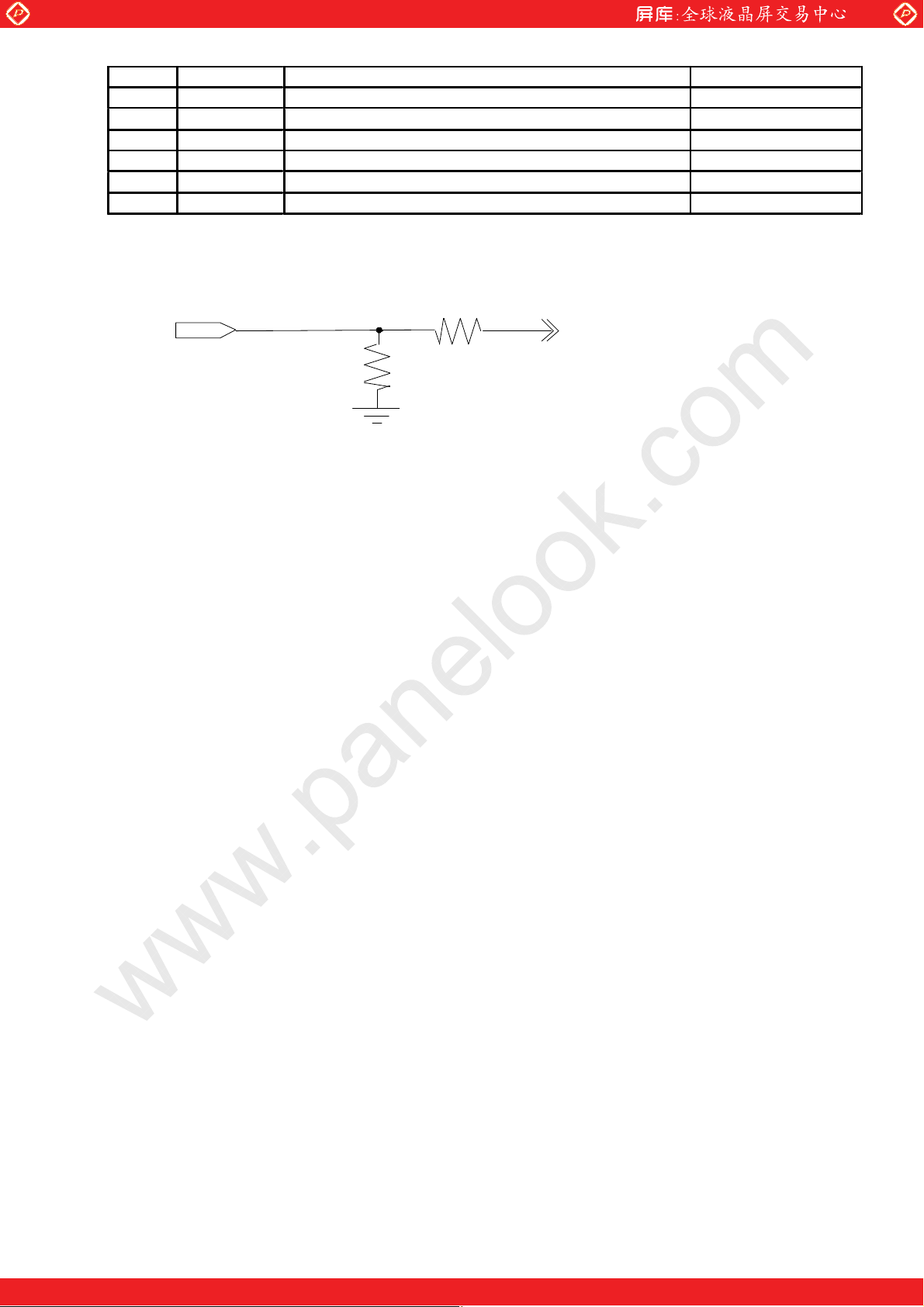
[Note 1]The equivalent circuit figure of the terminal
Terminal
www.panelook.com
LD- 20125-3
100Ω
10KΩ
One step solution for LCD / PDP / OLED panel application: Datasheet, inventory and accessory!
www.panelook.com
Page 6
Global LCD Panel Exchange Center
[Note 2] LVDS Data order
SELLVDS
Data
L(GND) or Open
www.panelook.com
LD- 20125-4
H(3.3V)
TA0
TA1
TA2
TA3
TA4
TA5
TA6
TB0
TB1
TB2
TB3
TB4
TB5
TB6
TC0
TC1
TC2
TC3
TC4 NA
TC5 NA
TC6
TD0
TD1
TD2
TD3
TD4
TD5
TD6
TE0
TE1
TE2
TE3
TE4
TE5
TE6
R2
R3
R4
R5
R6
R7
G2
G3
G4
G5
G6
G7
B2
B3
B4
B5
B6
B7
DE(*)
R8
R9(MSB)
G8
G9(MSB)
B8
B9(MSB)
NA
R0(LSB)
R1
G0(LSB)
G1
B0(LSB)
B1
NA
R4
R5
R6
R7
R8
R9(MSB)
G4
G5
G6
G7
G8
G9(MSB)
B4
B5
B6
B7
B8
B9(MSB)
NA
NA
DE(*)
R2
R3
G2
G3
B2
B3
N/A
R0(LSB)
R1
G0(LSB)
G1
B0(LSB)
B1
N/A
NA: Not Available
(*)Since the display position is prescribed by the rise of DE(Display Enable)signal, please do not fix DE
signal during operation at ”High”.
One step solution for LCD / PDP / OLED panel application: Datasheet, inventory and accessory!
www.panelook.com
Page 7
Global LCD Panel Exchange Center
www.panelook.com
LD- 20125-5
SELLVDS= Low (GND) or OPEN
ACK+,BCK+
–
,BCK
,BIN2
–
,BIN3
–
–
–
–
–
R3
G4
B5
R9
R2
G3
B4
R8
ACK
AIN0+,BIN0+
AIN0–,BIN0
AIN1+,BIN1+
AIN1–,BIN1
AIN2+,BIN2+
–
AIN2
AIN3+,BIN3+
AIN3
▲A
G2
B3
DE
NA
1 cycle
R7
B2
NA NA
B9 B8
R6
G7
R5
G6
B7
G9
R4
G5
B6
G8
R3
G4
B5
R9
R2
G3
B4
R8
G2
B3
DE
NA
AIN4+,BIN4+
AIN4–,BIN4
–
SELLVDS= High (3.3V)
ACK+,BCK+
ACK
–
,BCK
–
AIN0+,BIN0+
AIN0
–
,BIN0
–
AIN1+,BIN1+
–
,BIN1
–
,BIN2
–
,BIN3
–
–
–
AIN1
AIN2+,BIN2+
AIN2
AIN3+,BIN3+
AIN3
R1
R5
G6
B7
R3
R0
R4
G5
B6
R2
NA
G4
B5
DE
NA
B1
R9
B4
NA
B3
B0
R8
G9
NA
B2
G1
1 cycle
R7
G8
B9
G3
G0
R6
G7
B8
G2
R1
R5
G6
B7
R3
R0
R4
G5
B6
R2
NA
G4
B5
DE
NA
AIN4+,BIN4+
AIN4
–
,BIN4
–
R1
R0
NA
B1
B0
G1
G0
R1
R0
DE: Display Enable, NA: Not Available (Fixed Low)
One step solution for LCD / PDP / OLED panel application: Datasheet, inventory and accessory!
NA
www.panelook.com
Page 8

Global LCD Panel Exchange Center
R
R
[Note 3] The equivalent circuit figure of the
terminal
Terminal
4.2. Interface block diagram
GATE DRIVE
www.panelook.com
3.3V
4.7KΩ
100Ω
CN1
CONTROL PWB
Power Supply
Control Circuit
SOURCE DRIVER
LCD PANEL
1920×3(RGB)×1080
INPUT SIGNALS
O/S CONTROL
SIGNALS
POWER SUPPLY
GATE DRIVE
+12V DC
LD- 20125-6
SELLVDS
AIN0- AIN0+
AIN1- AIN1+
AIN2- AIN2+
AIN3- AIN3+
AIN4- AIN4+
ACK- ACK+
BIN0- BIN0+
BIN1- BIN1+
BIN2- BIN2+
BIN3- BIN3+
BIN4- BIN4+
BCK- BCK+
O/S SET
FRAME
ACK LIGHT(CCFT×24)
INPUT
SIGNALS
Von/off
Pdim
Pdim_sel
Balance Board
CN103,104
POWER SUPPLY
HV
One step solution for LCD / PDP / OLED panel application: Datasheet, inventory and accessory!
www.panelook.com
Page 9

Global LCD Panel Exchange Center
5. Measurement
To test Inverter need to warm up 30 minutes in the beginning, for lamp stability.
5.1 Block diagram
www.panelook.com
5.2 Test instrument
Item Function Instrument Type
1
2
3
4
5
6
Form No.: DFE0-01-001-04(030701)
A ΘDC CURRENT METER
A ΘRMS CURRENT METER
V ΘDIGITAL MULTI-METER
V ΘRMS VOLTAGE METER TDS 360 (Tektronix) or equivalentΔ
F ΘFERQUENCY COUNTER
O ΘOSCILLOSCOPE
FLUKE45 or equivalent
2016(YOKOGAWA) or FLUKE45 or P6022 AC
Current Probe(Tektronix) or equivalent
FLUKE45 or equivalent
PROBE 1137A(HP) or equivalent
5316A(HP) or equivalent
TDS 3012B (Tektronix)
One step solution for LCD / PDP / OLED panel application: Datasheet, inventory and accessory!
www.panelook.com
Page 10

Global LCD Panel Exchange Center
5.1. Interface connectors on the inverter
High voltage connector:
(CHN1~CHN2 and CN127~CN128 and CN226~CN227): JST_SM02B-BDAS-3-TB-2PIN or equivalent
(CHN101~CHN112 and CN113~CN124):Cvilux CP042CP1MC0
Connector PIN SYMBOL Description I/O
www.panelook.com
CHN1
CHN2
CN101
CN201
CHN101~CHN112
CN113~CN124
1 HV+ High Voltage Output
2 HV- High Voltage
1 HV+ High Voltage Output
2 HV- High Voltage
1 HV- High Voltage Input CN104
2 HV+ High Voltage Input
1 HV-
2 HV+ High Voltage
1 HV+ High Voltage Output
2 HV- High Voltage
1 HV+ High Voltage Output
2 HV- High Voltage
5.2 Feedback connector:
(CN114 ) ΚE&T_7151-E05N-00-R or equivalent
CN114
Pin NO
Name Description
High Voltage
Output
Output
InputCN203
Input
Output
Output
1FB
2
3NC
4
5
6
7
FB
GND
GND
LD
VCC
Lamp detected
Supply voltage
One step solution for LCD / PDP / OLED panel application: Datasheet, inventory and accessory!
www.panelook.com
Page 11

Global LCD Panel Exchange Center
5.3. The back light system characteristics
The back light system is direct type with 24 CCFTs (Cold Cathode Fluorescent Tube).
The characteristics of the lamp are shown in the following table. The value mentioned below is at the case of one
CCFT.
Item Symbol Min. Typ. Max. Unit Remarks
T
Life time
L
[Note]
• Lamp life time is defined as the time when brightness becomes 50% of the original value in the continuous
operation under the condition of Ta=25°C and brightness control=100%.
• Above value is applicable when the long side of LCD module is placed horizontally (Landscape position).
(Lamp lifetime may vary if LCD module is in portrait position due to the change of mercury density inside
the lamp.)
www.panelook.com
LD- 20125-9
- 60000 - Hour [Note]
One step solution for LCD / PDP / OLED panel application: Datasheet, inventory and accessory!
www.panelook.com
Page 12

Global LCD Panel Exchange Center
6. Electrical Characteristics
6.1. Control circuit driving
Parameter
Supply voltage
+12V supply
voltage
Permissible input ripple voltage V
Differential input
threshold voltage
Input High voltage
Input leak current (Low)
Input leak current (High)
[Note]V
CM
[Note 1]
Input voltage sequences Dip conditions for supply voltage
0 < t1 20ms
10 < t2 20ms
10 < t3 50ms
0 < t4 1s
t5 200ms
t6 0
t7 300ms
Current dissipation Icc
Inrush current
High
Low
Input Low voltage
Terminal resistor
: Common mode voltage of LVDS driver.
www.panelook.com
Ta=25 °C
Symbol
Vcc
I
RUSH
RUSH
T
RP
V
TH
V
TL
IL
V
V
IH
I
IL1
I
IL2
I
IH1
I
IH2
R
T
Dip conditions for supply voltage
is
Min.
11.4
-
-
Typ.
12
0.8
4.6
Max.
12.6
2.0
-
- 0.3 - ms [Note 7]
- - 100 mV
-
-100
0
2.3
-
-
-
-
-
-
-
-
-
-
-
-
-
100
100
-
1.0
3.3
400
40
40
400
-
a) 6.5V Vcc < 10.8V
td 10ms
b) Vcc < 6.5V
based on input voltage
sequence.
Uniit
V
A
A
P-P
mV
mV
V
V
µA
µA
µA
µA
Ω
LD- 20125-10
Remark
[Note 1]
[Note 2]
Vcc = +12.0V
VCM= +1.2V
[Note 6]
[Note 3]
V
I
= 0V
[Note 4]
V
I
= 0V
[Note 5]
V
I
= 3.3V
[Note 4]
I
= 3.3V
V
[Note 5]
Differential
input
0.9VCC
0.1Vcc
Vcc
t1
Data1 t2
Data2
Back light:V
ON
t3
t5
OFF
INV
t6
t4
t3
0.9Vcc
0.1Vcc
t7
OFF
0.1Vcc
Vcc
V1
V2
td
V1:10.8V
V2:6.5V
Ć Data1: ACK±, AIN0±, AIN1±, AIN2±, AIN3±, AIN4±,BCK±, BIN0±, BIN1±, BIN2±, BIN3±, BIN4
*V
voltage pursues the sequence mentioned above
CM
Ć Data2: SELLVDS, FRAME, O/S_SET
One step solution for LCD / PDP / OLED panel application: Datasheet, inventory and accessory!
www.panelook.com
Page 13

Global LCD Panel Exchange Center
[Note]About the relation between data input and back light lighting, please base on the above-mentioned input
sequence. When back light is switched on before panel operation or after a panel operation stop, it may not
display normally. But this phenomenon is not based on change of an incoming signal, and does not give
damage to a liquid crystal display.
[Note 2] Typical current situation: 256 gray-bar patterns. (Vcc = +12.0V)
The explanation of RGB gray scale is seen in section 8.
R G B R G B R G B
G S 0 G S 1 G S 2
. . . .
R G B
G S 2 5 4
www.panelook.com
LD- 20125-11
R G B
G S 2 5 5
Vcc˙+12.0V
CK˙74.25MHz
Th˙14.8μs
[Note 3] SELLVDS, FRAME, O/S_SET
[Note 4] O/S_SET
[Note 5] FRAME, SELLVDS
[Note 6] ACK±, AIN0±, AIN1±, AIN2±, AIN3±, AIN4±,BCK±, BIN0±, BIN1±, BIN2±, BIN3±, BIN4
[Note 7] Vcc12V inrush current waveform
t1 = 500us
Vcc
Irush = 4.6A
Icc
Trush = 300us
One step solution for LCD / PDP / OLED panel application: Datasheet, inventory and accessory!
www.panelook.com
Page 14

Global LCD Panel Exchange Center
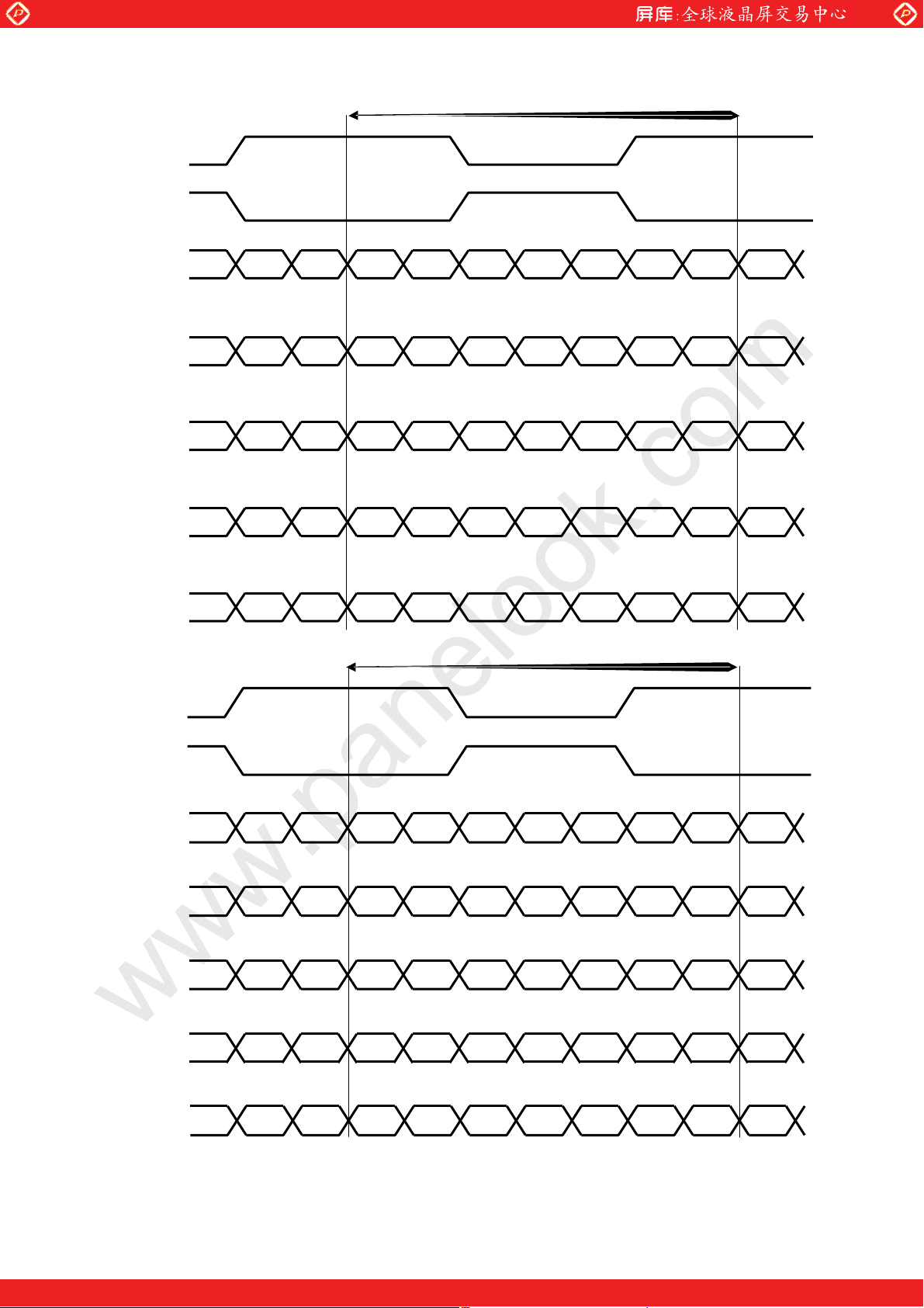
7. Timing characteristics of input signals
7.1. Timing characteristics
Timing diagrams of input signal are shown in Fig.2.
Parameter
Clock
Data enable
signal
[Note]-When vertical period is very long, flicker and etc. may occur.
-Please turn off the module after it shows the black screen.
-Please make sure that length of vertical period should become of an integral multiple of horizontal
length of period. Otherwise, the screen may not display properly.
-As for your final setting of driving timing, we will conduct operation check test at our side, please
inform your final setting.
Frequency
Horizontal period
Horizontal period (High)
Vertical period TV 1109 1125 1200 line
Vertical period (High) TVd 1080 1080 1080 line
www.panelook.com
Symbol Min.
1/Tc 67
TH
THd
1050
14.2
960
Typ.
74.25
1100
14.8
960
LD- 20125-13
Max. Unit Remark
76 MHz
1200 clock
16.1 µs
960 clock
DE
Aport DATA
(R,G,B)
Bport DATA
(R,G,B)
DE
1919
1920
Tc
TH
2
1
TV
THd
3
4
1 2
1919
1920
1079 1080
TVd
Fig.2 Timing characteristics of input signals
One step solution for LCD / PDP / OLED panel application: Datasheet, inventory and accessory!
www.panelook.com
Page 15

Global LCD Panel Exchange Center
7.2. Input data signal and display position on the screen
R1 G1 B1 R2 G2 B2
(ˍ㨮ˍ) (ˍ,ˎ)
ˍˍˍˎˍ ˏ 1㨯1920
ˎˍˎˎ
ˏˍ
1080㨯1
www.panelook.com
LD- 20125-14
R G B
1080㨯19 20
Display position of Dat (V,H)
One step solution for LCD / PDP / OLED panel application: Datasheet, inventory and accessory!
www.panelook.com
Page 16

Global LCD Panel Exchange Center
r
e
f
d
e
f
e
f
e
8. Input Signal, Basic Display Colors and Gray Scale of Each Color
Colors &
Gray scale
Black
Blue
Gray
R0 R1 R2 R3 R4 R5 R6 R7 R8 R9 G0 G1 G2 G3 G4 G5 G6 G7 G8 G9 B0 B1 B2 B3 B4 B5 B6 B7 B8 B9
Scale
– 0 0 0 0 0 0 0 0 0 0 0 0 0 0 0 0 0 0 0 0 0 0 0 0 0 0 0 0 0 0
– 0 0 0 0 0 0 0 0 0 0 0 0 0 0 0 0 0 0 0 0 1 1 1 1 1 1 1 1 1 1
www.panelook.com
LD- 20125-15
Data signal
Green
Cyan
Red
Basic Colo
Magenta – 1 1 1 1 1 1 1 1 1 1 0 0 0 0 0 0 0 0 0 0 1 1 1 1 1 1 1 1 1 1
Yellow – 1 1 1 1 1 1 1 1 1 1 1 1 1 1 1 1 1 1 1 1 0 0 0 0 0 0 0 0 0 0
White – 1 1 1 1 1 1 1 1 1 1 1 1 1 1 1 1 1 1 1 1 1 1 1 1 1 1 1 1 1 1
Black GS0 0 0 0 0 0 0 0 0 0 0 0 0 0 0 0 0 0 0 0 0 0 0 0 0 0 0 0 0 0 0
ǂ
Re
o
Darker GS2 0 1 0 0 0 0 0 0 0 0 0 0 0 0 0 0 0 0 0 0 0 0 0 0 0 0 0 0 0 0
ǂ
ǂ
Brighter GS1021 1 0 1 1 1 1 1 1 1 1 0 0 0 0 0 0 0 0 0 0 0 0 0 0 0 0 0 0 0 0
Gray Scal
ǂ
Red GS1023 1 1 1 1 1 1 1 1 1 1 0 0 0 0 0 0 0 0 0 0 0 0 0 0 0 0 0 0 0 0
Black GS0 0 0 0 0 0 0 0 0 0 0 0 0 0 0 0 0 0 0 0 0 0 0 0 0 0 0 0 0 0 0
ǂ
Green Gray Scal
Darker GS2 0 0 0 0 0 0 0 0 0 0 0 1 0 0 0 0 0 0 0 0 0 0 0 0 0 0 0 0 0 0
o
ǂ
ǂ
Brighter GS1021 0 0 0 0 0 0 0 0 0 0 1 0 1 1 1 1 1 1 1 1 0 0 0 0 0 0 0 0 0 0
Gray Scal
ǂ
Green GS1023 0 0 0 0 0 0 0 0 0 0 1 1 1 1 1 1 1 1 1 1 0 0 0 0 0 0 0 0 0 0
– 0 0 0 0 0 0 0 0 0 0 1 1 1 1 1 1 1 1 1 1 0 0 0 0 0 0 0 0 0 0
– 0 0 0 0 0 0 0 0 0 0 1 1 1 1 1 1 1 1 1 1 1 1 1 1 1 1 1 1 1 1
– 1 1 1 1 1 1 1 1 1 1 0 0 0 0 0 0 0 0 0 0 0 0 0 0 0 0 0 0 0 0
GS1 1 0 0 0 0 0 0 0 0 0 0 0 0 0 0 0 0 0 0 0 0 0 0 0 0 0 0 0 0 0
↓
↓
GS1022 0 1 1 1 1 1 1 1 1 1 0 0 0 0 0 0 0 0 0 0 0 0 0 0 0 0 0 0 0 0
GS1 0 0 0 0 0 0 0 0 0 0 1 0 0 0 0 0 0 0 0 0 0 0 0 0 0 0 0 0 0 0
↓
↓
GS1022 0 0 0 0 0 0 0 0 0 0 0 1 1 1 1 1 1 1 1 1 0 0 0 0 0 0 0 0 0 0
↓
↓
↓
↓
↓
↓
↓
↓
↓
↓
↓
↓
Black GS0 0 0 0 0 0 0 0 0 0 0 0 0 0 0 0 0 0 0 0 0 0 0 0 0 0 0 0 0 0 0
GS1 0 0 0 0 0 0 0 0 0 0 0 0 0 0 0 0 0 0 0 0 1 0 0 0 0 0 0 0 0 0
ǂ
Blu
Darker GS2 0 0 0 0 0 0 0 0 0 0 0 0 0 0 0 0 0 0 0 0 0 1 0 0 0 0 0 0 0 0
o
ǂ
ǂ
Brighter GS1021 0 0 0 0 0 0 0 0 0 0 0 0 0 0 0 0 0 0 0 0 1 0 1 1 1 1 1 1 1 1
ǂ
Blue GS1023 0 0 0 0 0 0 0 0 0 0 0 0 0 0 0 0 0 0 0 0 1 1 1 1 1 1 1 1 1 1
↓
↓
GS1022 0 0 0 0 0 0 0 0 0 0 0 0 0 0 0 0 0 0 0 0 0 1 1 1 1 1 1 1 1 1
↓
↓
↓
↓
0: Low level voltage, 1: High level voltage.
Each basic color can be displayed in 1024 gray scales from 10 bits data signals. According to the combination of
total 30 bits data signals, the TBD-color display can be achieved on the screen.
One step solution for LCD / PDP / OLED panel application: Datasheet, inventory and accessory!
↓
↓
www.panelook.com
Page 17

Global LCD Panel Exchange Center
9. Optical characteristics
Parameter Symbol Condition Min. Typ. Max. Unit Remark
Horizontal
Viewing angle
range
Contrast ratio CRn 1000 1500 - [Note2,4]
Response time
Chromaticity
Luminance White 360 450 - -
Luminance
uniformity
Measurement condition: Set the value of V
*The measurement shall be executed 60 minutes after lighting at rating.
Vertical
White
Red
Green
Blue
White δw - - 1.25 cd/m
www.panelook.com
INV =
Ta=25°C, Vcc=12.0V, V
θ
21 70 88 - Deg.
θ
22
θ 11
CR10
70 88 -
24.0V, V
θ 12
τ
r
τ
d
x
y
x
y
θ =0 deg.
x
y
x
y
to maximum luminance of white.
BRT
- 6 - ms [Note3,4,5]
0.242 0.272 0.302
0.247 0.277 0.307
0.610 0.640 0.670
0.300 0.330 0.360
0.250 0.280 0.310
0.570 0.600 0.630
0.120 0.150 0.180
0.030 0.060 0.090
=100%ˈTiming:60Hz(typ. value)
BRT
Deg.
LD- 20125-16
[Note1,4]
-
-
-
-
-
[Note4]
-
-
-
2
[Note 6]
[Note]The optical characteristics are measured using the following equipment.
Detector˄SR-3˅
Detector˄EZ-CONTRAST/ Photodiode˅
400mm
Field=1°
Middle of the screen (θ˙0°)
TFT-LCD Module
Fig.4-1 Measurement of viewing angle range and
Response time.
Fig.4-2 Measurement of Contrast, Luminance,
Middle of the screen (θ˙0°)
TFT-LCD Module
Chromaticity.
Viewing angle range: EZ-CONTRAST
Response time: Photodiode
One step solution for LCD / PDP / OLED panel application: Datasheet, inventory and accessory!
www.panelook.com
Page 18

Global LCD Panel Exchange Center
r
t
[Note 1]Definitions of viewing angle range :
θ 22
θ 12
[Note 2]Definition of contrast ratio :
The contrast ratio is defined as the following.
www.panelook.com
Normal line
θ 11
6 o’clock direction
LD- 20125-17
θ 21
Luminance (brightness) with all pixels white
Contrast Ratio
˙
Luminance (brightness) with all pixels black
[Note 3]Definition of response time
The response time (τ
and τr) is defined as the following figure and shall be measured by switching the input
d
signal for “any level of gray (0%, 25%, 50%, 75% and 100%)” and “any level of gray (0%, 25%, 50%, 75%
and 100%)”.
0%
25ˁ
50ˁ
75ˁ
100%
0% 25ˁ
tr:0%-25ˁ
td: 25%-0ˁ
td: 50%-0ˁ td: 50%-25ˁ
td: 75%-0ˁ td: 75%-25ˁ td: 75%-50ˁ
td: 100%-0ˁ td: 100%-25ˁ td: 100%-50ˁ td:100%-75ˁ
50ˁ
tr:0%-50%
tr: 25%-50ˁ tr25%-75ˁ tr: 25%-100ˁ
75ˁ
tr:0%-75%
tr: 50%-75ˁ tr: 50%-100ˁ
100%
tr:0%-100%
tr: 75%-100ˁ
t*:x-y...response time from level of gray(x) to level of gray(y)
τ
= Σ(tr:x-y)/10 , τd= Σ(td:x-y)/10
r
Bright Dark
100%
90%
Bright
Photodetecto
Outpu
10%
0%
τ
d
time
τ
r
[Note 4]This shall be measured at center of the screen.
[Note 5] This value is valid when O/S driving is used at typical input time value.
One step solution for LCD / PDP / OLED panel application: Datasheet, inventory and accessory!
www.panelook.com
Page 19

Global LCD Panel Exchange Center
[Note 6]Definition of white uniformity ;
White uniformity is defined as the following with five measurements. (Aѝ E)
www.panelook.com
LD- 20125-18
Maximum luminance of five points (brightness)
δ
˳
˙
480 960 1440
pixel
Minimum luminance of five points (brightness)
A
B
D
C
E
270
540
810
pixel
10. Handling Precautions of the module
a) Be sure to turn off the power supply when inserting or disconnecting the
cable.
b) This product is using the parts (inverter, CCFT etc), which generate the high voltage.
Therefore, during operating, please don't touch these parts.
c) Brightness control voltage is switched for “ON” and “OFF”, as shown in Fig.4. Voltage difference generated
by this switching, ΔV
inverter and its surrounding circuit. So, separate the power supply of the inverter circuit with the one of its
surrounding circuit.
INV,
may affect a sound output, etc. when the power supply is shared between the
ΔV
INV
V
INV
I
INV
PWM control
signal
0V
0A
ON OFF ON
0V
Fig.4 Brightness control voltage.
*Since inverter board’s GND is not connected to the frame of the LCD module, please connect it with the
Customer’s GND of inverter power supply.
d) Be sure to design the cabinet so that the module can be installed without any extra stress such as warp or
twist.
e) Since the front polarizer is easily damaged, pay attention not to scratch it.
f) Since long contact with water may cause discoloration or spots, wipe off water drop immediately.
g) When the panel surface is soiled, wipe it with absorbent cotton or other soft cloth.
h) Since the panel is made of glass, it may break or crack if dropped or bumped on hard surface. Handle with
care.
One step solution for LCD / PDP / OLED panel application: Datasheet, inventory and accessory!
www.panelook.com
Page 20

Global LCD Panel Exchange Center
i) Since CMOS LSI is used in this module, take care of static electricity and take the human earth into
consideration when handling.
j) The module has some printed circuit boards (PCBs) on the back side, take care to keep them form any stress
or pressure when handling or installing the module; otherwise some of electronic parts on the PCBs may be
damaged.
k) Observe all other precautionary requirements in handling components.
l) When some pressure is added onto the module from rear side constantly, it causes display non-uniformity
issue, functional defect, etc. So, please avoid such design.
m) When giving a touch to the panel at power on supply, it may cause some kinds of degradation. In that case,
once turn off the power supply, and turn on after several seconds again, and that is disappear.
n) When handling LCD modules and assembling them into cabinets, please be noted that long-term storage in
the environment of oxidization or deoxidization gas and the use of such materials as reagent, solvent,
adhesive, resin, etc. which generate these gasses, may cause corrosion and discoloration of the LCD
modules.
o) This LCD module is designed to prevent dust from entering into it. However, there would be a possibility to
have a bad effect on display performance in case of having dust inside of LCD module. Therefore,
please ensure to design your TV set to keep dust away around LCD module.
www.panelook.com
LD- 20125-19
11. Packing form
a) Piling number of cartons:2 maximum
b) Packing quantity in one carton:3pcs
c) Carton size:1320(W) × 300(D) × 830(H)
d) Total mass of one carton filled with full modules: 75kg(Max)
12. Reliability test item
No.
1
2
3
4
5
High temperature storage test
Low t emperature storage test
High temperature and high humidity
High temperature operation test
Low t emperature operation test
6
7
8
[Result evaluation criteria]
Under the display quality test condition with normal operation state, there shall be no change, which may
affect practical display function.
Test item
operation test
Vibration test
(non-operation)
Shock test
(non-operation)
ESD
Ta=60°C 240h
Ta=-25°C 240h
Ta=40°C ; 95%RH
(No condensation)
Ta=50°C 240h
Ta=0°C 240h
Frequency: 10~57Hz/Vibration width (one side): 0.075mm
: 58~500Hz/Acceleration: 9.8 m/s²
Sweep time: 11 minutes
Test period: 3 hours (1h for each direction of X, Y, Z)
Maximum acceleration: 294m/s
Pulse width: 11ms, sinusoidal half wave
Direction: +/-X, +/-Y, +/-Z, once for each direction.
* At the following conditions, it is a thing without incorrect
operation and destruction.
(1)Non-operation: Contact electric discharge ±10kV
(2)Operation Contact electric discharge ±8kV
Condition
240h
2
Non-contact electric discharge ±20kV
Non-contact electric discharge ±15kV
Conditions: 150pF, 330ohm
One step solution for LCD / PDP / OLED panel application: Datasheet, inventory and accessory!
www.panelook.com
Page 21

Global LCD Panel Exchange Center
13. Others
1) Lot No. Label ;
The label that displays SHARP, product model (LK520D1LH00), a product number is stuck on the back of the
module.
ǏLK520D1LH00X,TǐNSEC PRODUCTION
www.panelook.com
LD- 20125-20
˨˧5
˔ˍ ˯ˌˌˌˌˍ X
˄orT˅
A production year(the last figures of the Christian Era)
2) Packing Labe
ǏLK520D1LH00ǐ
20 D1LH00
Module No.
Barcode
Lot No.
A production month (1-9, X,Y, Z)
How to express Lot No.
○○ ○○
○ ○ ○ ○
Serial No.
Management No.
Identification Code
N:NSEC
⼒ݙક⬾˖˄ː˯˅
LK520D1LH00X(orT)
(ķ)
Bar code
˨˪˫ˊ
˄ˍ˰˅ˎˌˌ˔. ˆ.ˆˆ (ĸ)
Bar code
˭˽˖
˄˭˅
˔ ˿ (Ĺ)
Bar code
ɮόȾક⬾ ˖
ȿɫόɟ⠽⌕⫼ɱɡɳǼǮDŽ
ķ Management No.
ĸ Lot No. (Date)
Ĺ Quantity
3) Adjusting volume has been set optimally before shipment, so do not change any adjusted value.
If adjusted value is changed, the specification may not be satisfied.
4) Disassembling the module can cause permanent damage and should be strictly avoided.
5) Please be careful since image retention may occur when a fixed pattern is displayed for a long time.
One step solution for LCD / PDP / OLED panel application: Datasheet, inventory and accessory!
www.panelook.com
Page 22

Global LCD Panel Exchange Center
6) The chemical compound, which causes the destruction of ozone layer, is not being used.
7) Cold cathode fluorescent lamp in LCD PANEL contains a small amount of mercury. Please follow local
ordinances or regulations for disposal. This sentence is displayed on the backside of the module.
8) When any question or issue occurs, it shall be solved by mutual discussion.
9) This module is corresponded to RoHS.
14. Carton storage condition
TemperatureC to 40°C
Humidity 95%RH or less
Reference condition : 20°C to 35°C, 85%RH or less (summer)
: 5°C to 15°C, 85%RH or less (winter)
Sunlight
Atmosphere
Notes
Storage life
Be sure to shelter a product from the direct sunlight.
Harmful gas, such as acid and alkali which bites electronic components and/or
wires must not be detected.
Be sure to put cartons on palette or base, don’t put it on floor, and store them with
removing from wall
Please take care of ventilation in storehouse and around cartons, and control
changing temperature is within limits of natural environment
1 year
www.panelook.com
LD- 20125-21
• the total storage time (40°C,95%RH) : 240H or less
One step solution for LCD / PDP / OLED panel application: Datasheet, inventory and accessory!
www.panelook.com
 Loading...