

Page 1
Global LCD Panel Exchange Center
SPECIFICATION
PREPARED BY: DATE
APPROVED BY: DATE ISSUE: Dec, 2, 2011
LIQUID CRYSTAL DISPLAY GROUP
SHARP CORPORATION
www.panelook.com
SPEC No. LD-K23Z01
FILE No.
PAGE : 26 pages
APPLICABLE GROUP
LIQUID CRYSTAL DISPLAY GROUP
DEVICE SPECIFICATION FOR 㻌
㻌
TFT - LCD module㻌
MODEL No. LQ038Q5DRQ1
CUSTOMER'S APPROVAL
DATE
PRESENTED
BY
6+$53&25325$7,21
BY
LK400D3LC03
.7DQDND
$66,67$17'(3$570(17*(1(5$/0$1$*(5
'(9(/230(17'(3$570(17
/,48,'&5<67$/',63/$<*5283
One step solution for LCD / PDP / OLED panel application: Datasheet, inventory and accessory!
www.panelook.com
Page 2
Global LCD Panel Exchange Center
RECORDS OF REVISION
MODEL No. : LK400D3LC03
SPEC No. : LD-K23Z01
www.panelook.com
DATE
NO.
2011.12.2 LD-K23Z01
REVISED
No.
㸫㸫
PAGE SUMMARY NOTE
㸫
1st Issue
One step solution for LCD / PDP / OLED panel application: Datasheet, inventory and accessory!
www.panelook.com
Page 3
Global LCD Panel Exchange Center
r
m
1. Application
This specification applies to the color 40.0” TFT-LCD module LK400D3LC03.
* These specifications are proprietary products of SHARP CORPORATION (“SHARP”) and include materials
protected under copyright of SHARP. Do not reproduce or cause any third party to reproduce them in any form or
by any means, electronic or mechanical, for any purpose, in whole or in part, without the express written
permission of SHARP.
* In case of using the device for applications such as control and safety equipment for transportation (aircraft, trains,
automobiles, etc.), rescue and security equipment and various safety related equipment which require higher
reliability and safety, take into consideration that appropriate measures such as fail-safe functions and redundant
system design should be taken.
* Do not use the device for equipment that requires an extreme level of reliability, such as aerospace applications,
telecommunication equipment (trunk lines), nuclear power control equipment and medical or other equipment for
life support.
* SHARP assumes no responsibility for any damage resulting from the use of the device that does not comply with
the instructions and the precautions specified in these specifications.
* Contact and consult with a SHARP sales representative for any questions about this device.
2. Overview
This module is a color active matrix LCD module incorporating amorphous silicon TFT (Thin Film Transistor). It
is composed of a color TFT-LCD panel, driver ICs, control circuit, and edge-lit LED backlight system etc. Graphics
and texts can be displayed on a 1920RGB1080 dots panel with one billion colors (RGB 10bits) by using LVDS
(L
ow Voltage Differential Signaling) to interface, +12V of DC supply voltages.
And in order to improve the response time of LCD, this module applies the Over Shoot driving (O/S driving)
technology for the control circuit. In the O/S driving technology, signals are being applied to the Liquid Crystal
according to a pre-fixed process as an image signal of the present frame when a difference is found between image
signal of the previous frame and that of the current frame after comparing them.
With this technology, image signals can be set so that liquid crystal response completes within one frame. As a
result, motion blur reduces and clearer display performance can be realized
This LCD module also adopts Double Frame Rate driving method.
With combination of these technologies, motion blur can be reduced and clearer display performance can be
realized.
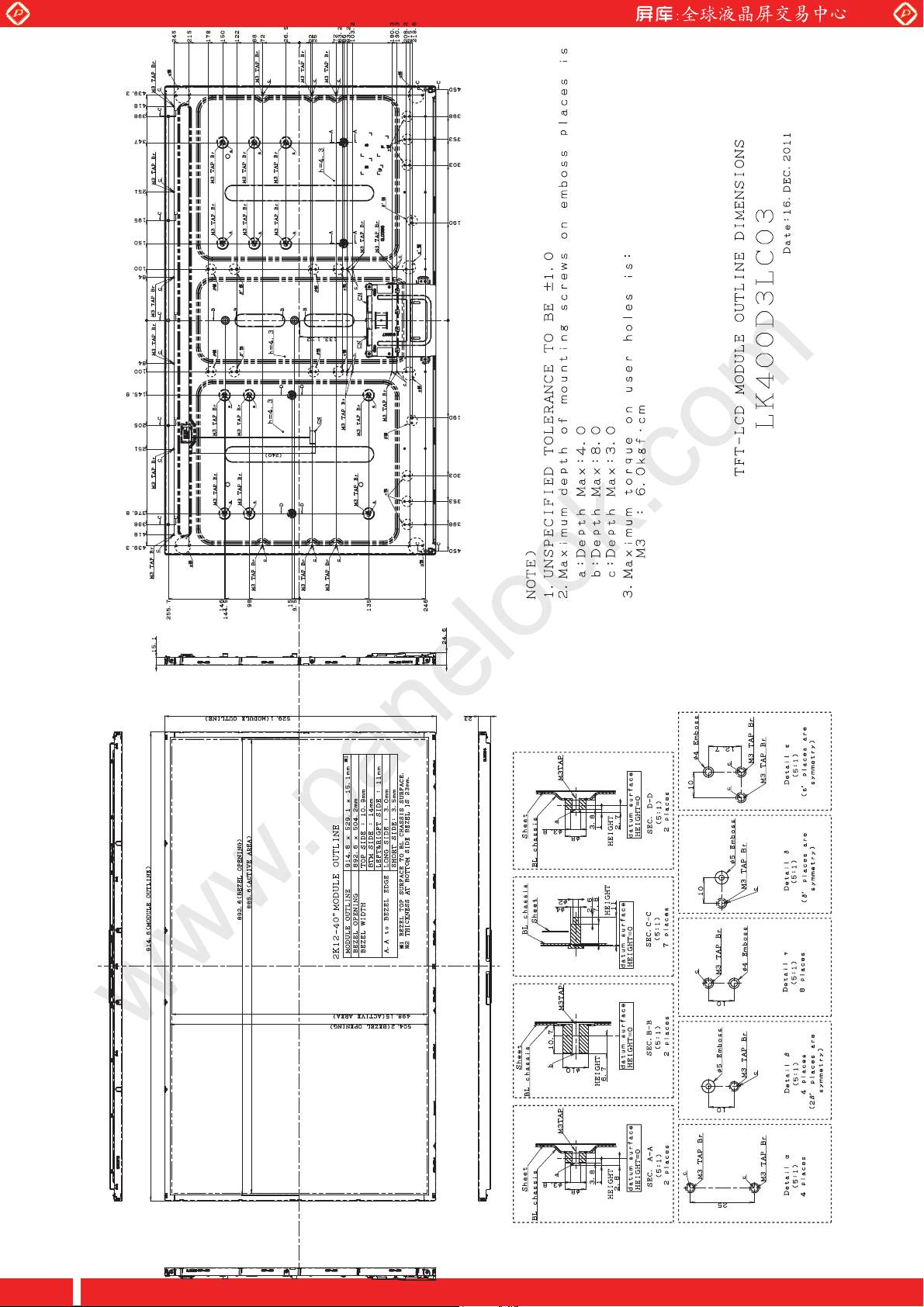
3. Mechanical Specifications
Paramete
Display size
Active area 885.6(H) x 498.15 (V) mm
Pixel Format
Pixel pitch 0.15375(H) x 0.46125 (V) mm
Pixel configuration R, G, B vertical stripe
Display mode Normally black
Unit Outline Dimensions (*1) 914.6(W) x 529.1(H) x 10.8(D) mm
Mass
Surface treatment
(*1) Outline is shown in Fig.1
www.panelook.com
Specifications Unit
101.609 㸦Diagonal㸧
40.0 㸦Diagonal㸧
1920(H) x 1080(V)
㸦1pixel = R + G + B dot㸧
7.6s1.0
Low-Haze Anti Glare
Hard coating: 3H and more
Haze value : 7% (typ)
LD-K23Z01-1
c
inch
pixel
kg
One step solution for LCD / PDP / OLED panel application: Datasheet, inventory and accessory!
www.panelook.com
Page 4
Global LCD Panel Exchange Center
4. Input Terminals
4.1. TFT panel driving
CN1 (Interface signals and +12V DC power supply)
Using connector : 91213-0510 (Aces Electronics Co., Ltd.)
Mating connector : FI-RE51HL, FI-RE51CL (Japan Aviation Electronics Ind., Ltd.)
Mating LVDS transmitter : THC63LVD1023 or equivalent device
Pin No. Symbol Function Remark
1
2
3
4
5
6
7
8
9
10
11
12
13
14
15
16
17
18
19
20
21
22
23
24
25
26
27
28
29
30
31
32
33
34
35
36
37
38
39
40
41
42
43
44
NC Non-connection (default : OPEN)
I2C_SDA I2C data signal [Note 1]
I2C_SCL I2C clock signal [Note 1]
Reserved Non-connection (default : OPEN)
R/W
Reserved Non-connection (default : OPEN) Open
SELLVDS
Reserved Non-connection (default : OPEN) Open
Reserved Non-connection (default : OPEN) Open
Reserved Non-connection (default : OPEN) Open
GND
AIN0- Aport (-)LVDS CH0 differential data input
AIN0+ Aport (+)LVDS CH0 differential data input
AIN1- Aport (-)LVDS CH1 differential data input
AIN1+ Aport (+)LVDS CH1 differential data input
AIN2- Aport (-)LVDS CH2 differential data input
AIN2+ Aport (+)LVDS CH2 differential data input
GND
ACK- Aport LVDS Clock signal(-)
ACK+ Aport LVDS Clock signal(+)
GND
AIN3- Aport (-)LVDS CH3 differential data input
AIN3+ Aport (+)LVDS CH3 differential data input
AIN4- Aport (-)LVDS CH4 differential data input
AIN4+ Aport (+)LVDS CH4 differential data input
GND
GND
BIN0- Bport (-)LVDS CH0 differential data input
BIN0+ Bport (+)LVDS CH0 differential data input
BIN1- Bport (-)LVDS CH1 differential data input
BIN1+ Bport (+)LVDS CH1 differential data input
BIN2- Bport (-)LVDS CH2 differential data input
BIN2+ Bport (+)LVDS CH2 differential data input
GND
BCK- Bport LVDS Clock signal(-)
BCK+ Bport LVDS Clock signal(+)
GND
BIN3- Bport (-)LVDS CH3 differential data input
BIN3+ Bport (+)LVDS CH3 differential data input
BIN4- Bport (-)LVDS CH4 differential data input
BIN4+ Bport (+)LVDS CH4 differential data input
GND
GND
GND
Read/write enable for TCON ROM
(Low : Disenable, High : Enable)
Select LVDS data order [Note2]
www.panelook.com
LD-K23Z01-2
Open *If the 0Ȑ is mounted on the R128,
Pin No.1 is connected to GND.
Slave address㸸B4 / Pull up (3.3[V])
Slave address㸸B4 / Pull up (3.3[V])
Pull down (GND) [Note 3]
Pull down (GND) [Note 3]
One step solution for LCD / PDP / OLED panel application: Datasheet, inventory and accessory!
www.panelook.com
Page 5
Global LCD Panel Exchange Center
45
46
47
48
49
50
51
CN2 (Interface signals)
Using connector : 91213-0410 (Aces Electronics Co., Ltd.)
Mating connector : FI-RE41HL, FI-RE41CL (Japan Aviation Electronics Ind., Ltd.)
Pin No. Symbol Function Remark
1
2
3
4
5
6 Reserved
7 Reserved
8 Reserved
9 GND
10
11
12
13
14
15
16
17
18
19
20
21
22
23
24
25
26
27
28
29
30
31
32
33
34
35
36
37
38
39
40
41
[Note] GND of a liquid crystal panel drive part has connected with a module chassis.
GND
GND
Reserved Non-connection (default : OPEN)
VCC +12V Power Supply
VCC +12V Power Supply
VCC +12V Power Supply
VCC +12V Power Supply
Reserved (VCC) +12V Power Supply
Reserved (VCC) +12V Power Supply
Reserved (VCC) +12V Power Supply
Reserved Non-connection (default : OPEN)
Reserved Non-connection (default : OPEN)
CIN0- Cport (-)LVDS CH0 differential data input
CIN0+ Cport (+)LVDS CH0 differential data input
CIN1- Cport (-)LVDS CH1 differential data input
CIN1+ Cport (+)LVDS CH1 differential data input
CIN2- Cport (-)LVDS CH2 differential data input
CIN2+ Cport (+)LVDS CH2 differential data input
GND
CCK- Cport LVDS Clock signal(-)
CCK+ Cport LVDS Clock signal(+)
GND
CIN3- Cport (-)LVDS CH3 differential data input
CIN3+ Cport (+)LVDS CH3 differential data input
CIN4- Cport (-)LVDS CH4 differential data input
CIN4+ Cport (+)LVDS CH4 differential data input
GND
GND
DIN0- Dport (-)LVDS CH0 differential data input
DIN0+ Dport (+)LVDS CH0 differential data input
DIN1- Dport (-)LVDS CH1 differential data input
DIN1+ Dport (+)LVDS CH1 differential data input
DIN2- Dport (-)LVDS CH2 differential data input
DIN2+ Dport (+)LVDS CH2 differential data input
GND
DCK- Dport LVDS Clock signal(-)
DCK+ Dport LVDS Clock signal(+)
GND
DIN3- Dport (-)LVDS CH3 differential data input
DIN3+ Dport (+)LVDS CH3 differential data input
DIN4- Dport (-)LVDS CH4 differential data input
DIN4+ Dport (+)LVDS CH4 differential data input
GND
GND
www.panelook.com
LD-K23Z01-3
Non-connection (default : OPEN)
Non-connection (default : OPEN)
Non-connection (default : OPEN)
One step solution for LCD / PDP / OLED panel application: Datasheet, inventory and accessory!
www.panelook.com
Page 6
Global LCD Panel Exchange Center
[Note 1] Slave address “9E” is allocated for internal use for TCON board.
The equivalent circuit figure of the terminal
Te rm in al
www.panelook.com
LD-K23Z01-4
[Note 2] LVDS Data order
Data
TA0
TA1
TA2
TA3
TA4
TA5
TA6
TB0
TB1
TB2
TB3
TB4
TB5
TB6
TC0
TC1
TC2
TC3
TC4 N/A N/A
TC5 N/A N/A
TC6 DE(*) DE(*)
TD0
TD1
TD2
TD3
TD4
TD5
TD6
TE0
TE1
TE2
TE3
TE4
TE5
TE6
N/A: Not Available
(*)Since the display position is prescribed by the rise of DE(Display Enable)signal, please do not fix DE
signal during operation at ”High”.
100
10KȐ
SELLVDS
L(GND) or Open [VESA㸪NS]
R0(LSB)㻌
R1㻌
R2㻌
R3㻌
R4㻌
R5㻌
G0(LSB)㻌
G1㻌
G2㻌
G3㻌
G4㻌
G5㻌
B0(LSB)㻌
B1㻌
B2㻌
B3㻌
B4㻌
B5㻌
R6㻌
R7㻌
G6㻌
G7㻌
B6㻌
B7㻌
N/A㻌
R8㻌
R9(MSB)㻌
G8㻌
G9(MSB)㻌
B8㻌
B9(MSB)㻌
N/A㻌
H(3.3V) [JEIDA]
R4
R5
R6
R7
R8
R9(MSB)
G4
G5
G6
G7
G8
G9(MSB)
B4
B5
B6
B7
B8
B9(MSB)
R2
R3
G2
G3
B2
B3
N/A
R0(LSB)
R1
G0(LSB)
G1
B0(LSB)
B1
N/A
One step solution for LCD / PDP / OLED panel application: Datasheet, inventory and accessory!
www.panelook.com
Page 7
Global LCD Panel Exchange Center
[Note 3] LVDS Data order
SELLVDS
Data L(GND) or Open
[VESA]
TA0
TA1
TA2
TA3
TA4
TA5
TA6
TB0
TB1
TB2
TB3
TB4
TB5
TB6
TC0
TC1
TC2
TC3
TC4 NA NA
TC5 NA NA
TC6 DE(*) DE(*)
TD0
TD1
TD2
TD3
TD4
TD5
TD6
TE0
TE1
TE2
TE3
TE4
TE5
TE6
NA: Not Available
(*)Since the display position is prescribed by the rise of DE(Display Enable)signal, please do not fix DE
signal during operation at ”High”.
R0(LSB)㻌
R1㻌
R2㻌
R3㻌
R4㻌
R5㻌
G0(LSB)㻌
G1㻌
G2㻌
G3㻌
G4㻌
G5㻌
B0(LSB)㻌
B1㻌
B2㻌
B3㻌
B4㻌
B5㻌
R6㻌
R7㻌
G6㻌
G7㻌
B6㻌
B7㻌
N/A㻌
R8㻌
R9(MSB)㻌
G8㻌
G9(MSB)㻌
B8㻌
B9(MSB)㻌
N/A㻌
www.panelook.com
LD-K23Z01-5
H(3.3V)
[JEIDA]
R4
R5
R6
R7
R8
R9(MSB)
G4
G5
G6
G7
G8
G9(MSB)
B4
B5
B6
B7
B8
B9(MSB)
R2
R3
G2
G3
B2
B3
N/A
R0(LSB)
R1
G0(LSB)
G1
B0(LSB)
B1
N/A
One step solution for LCD / PDP / OLED panel application: Datasheet, inventory and accessory!
www.panelook.com
Page 8
Global LCD Panel Exchange Center
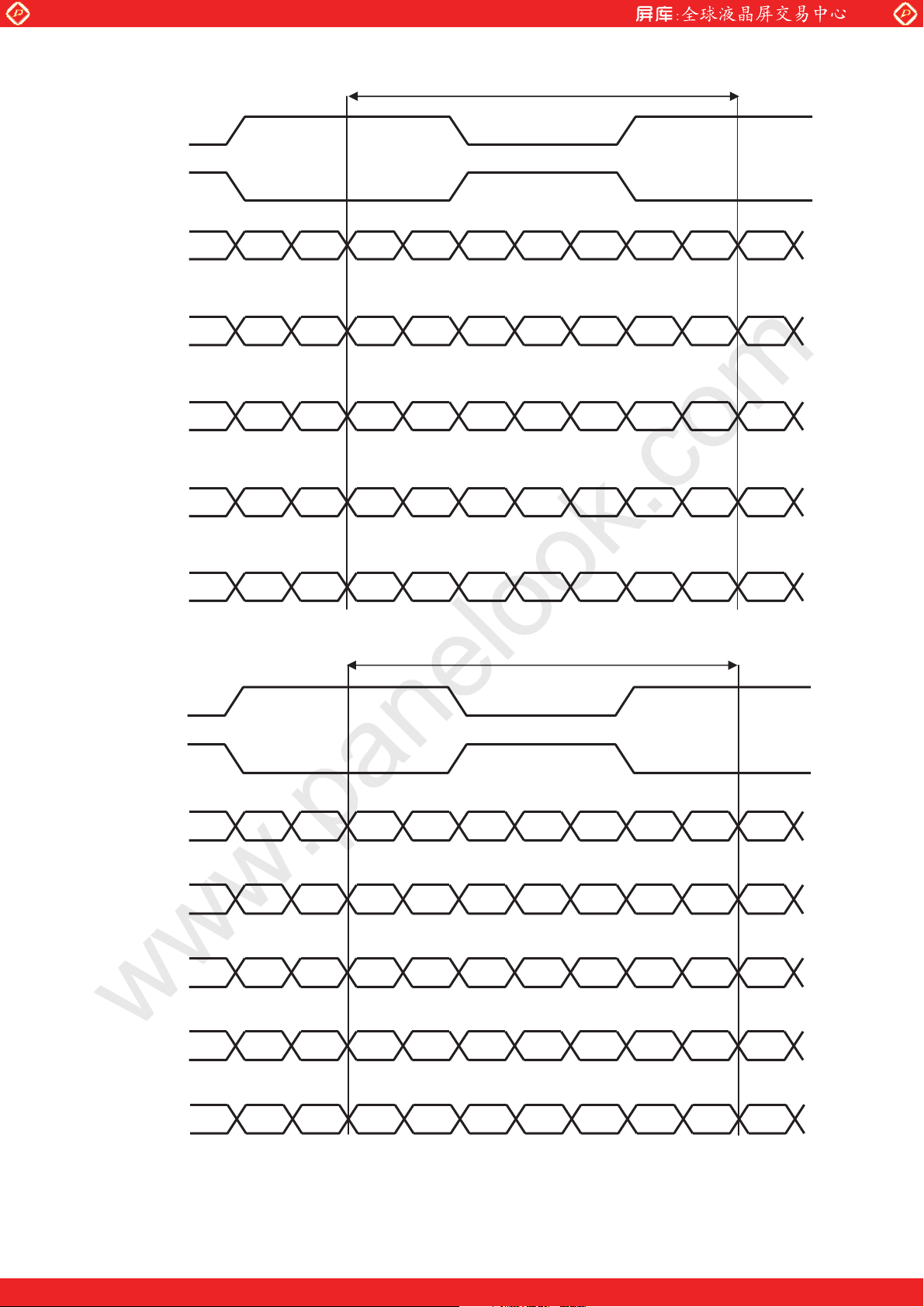
SELLVDS= Low (GND) or OPEN
ACK+,BCK+
ACK– ,BCK–
AIN0+,BIN0+
–,BIN0–
AIN0
AIN1+,BIN1+
–,BIN1–
AIN1
AIN2+,BIN2+
–,BIN2–
AIN2
AIN3+,BIN3+
–,BIN3–
AIN3
AIN4+,BIN4+
–,BIN4–
AIN4
www.panelook.com
LD-K23Z01-6
1 cycle
G0 R5 R4 R3 R2 R1 R0 R0 R1 G0
B1 B0 G5 G4 G3 G2 G1 G1 G2 B1
DE
NA NA
B7 B6 G7 G6 R7 R6 R6 R7 NA NA
B9 B8 G9 G8 R9 R8 R8 R9 NA NA
B5 B4 B3 B2 B2 B3
DE
SELLVDS= High (3.3V)
ACK+,BCK+
ACK– ,BCK–
AIN0+,BIN0+
–,BIN0–
AIN0
AIN1+,BIN1+
–,BIN1–
AIN1
AIN2+,BIN2+
–,BIN2–
AIN2
AIN3+,BIN3+
AIN3
–,BIN3–
AIN4+,BIN4+
–,BIN4–
AIN4
DE: Display Enable, NA: Not Available (Fixed Low)
1 cycle
G4 R9 R8 R7 R6 R5 R4 R4 R5 G4
B5 B4 G9 G8 G7 G6 G5 G5 G6 B5
DE
NA NA
B3 B2 G3 G2 R3 R2 R2 R3 NA NA
B1 B0 G1 G0 R1 R0 R0 R1 NA NA
B9 B8 B7 B6 B6 B7
DE
One step solution for LCD / PDP / OLED panel application: Datasheet, inventory and accessory!
www.panelook.com
Page 9
Global LCD Panel Exchange Center
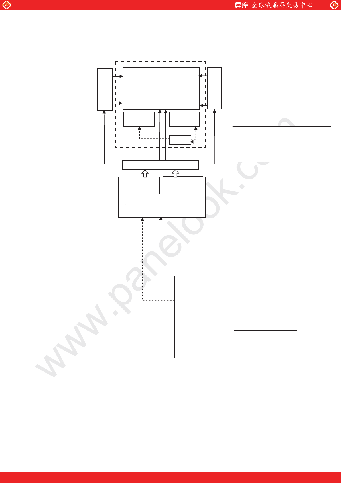
㻵㻺㻼㼁㼀㻌㻿㻵㻳㻺㻭㻸㻿㻌
㻼㻻㼃㻱㻾㻌㻿㼁㻼㻼㻸㼅
㻌
㻌
㻌
㻌
㻌
㻌
㻌
㻌
㻌
㻌
㻸㻯㻰㻌㻼㻭㻺㻱㻸㻌
㻝㻥㻞㻜㽢㻟㻔㻾㻳㻮㻕㽢㻝㻜㻤㻜㻌
㻳㻭㼀㻱㻌㻰㻾㻵㼂㻱㻾㻌
㻳㻭㼀㻱㻌㻰㻾㻵㼂㻱㻾㻌
㻯㻻㻺㼀㻾㻻㻸㻌㻼㼃㻮㻌
㼓
㻿㻻㼁㻾㻯㻱 㻰㻾㻵㼂㻱㻾
㻼㻻㼃㻱㻾㻌㻿㼁㻼㻼㻸㼅㻌
㻸㻱㻰㻌㻼㼃㻮
㻸㻱㻰㻌㻼㼃㻮
㻱㼐㼓㼑㻙㼘㼕㼠㻌㻮㼍㼏㼗㻌㻸㼕㼓㼔㼠
㻵㻺㻼㼁㼀㻌㻿㻵㻳㻺㻭㻸㻿
4.2. Interface block diagram
www.panelook.com
㻌
㻌
㻌
㻯㼛㼚㼠㼞㼛㼘㻌
㼚㼍㼘㼟
㻿㼕
㻯㻺㻞㻌
㻼㼛㼣㼑㼞㻌㻿㼡㼜㼜㼘㼥
㻯㼕㼞㼏㼡㼕㼠㻌
㻯㻺㻝㻌
㻯㻵㻺㻜㻙㻌㻯㻵㻺㻜㻗㻌
㻯㻵㻺㻝㻙㻌㻯㻵㻺㻝㻗㻌
㻯㻵㻺㻞㻙㻌㻯㻵㻺㻞㻗㻌
㻯㻵㻺㻟㻙㻌㻯㻵㻺㻟㻗㻌
㻯㻵㻺㻠㻙㻌㻯㻵㻺㻠㻗㻌
㻯㻯㻷㻙㻌㻯㻯㻷㻗㻌
㻰㻵㻺㻜㻙㻌㻰㻵㻺㻜㻗㻌
㻰㻵㻺㻝㻙㻌㻰㻵㻺㻝㻗㻌
㻰㻵㻺㻞㻙㻌㻰㻵㻺㻞㻗㻌
㻰㻵㻺㻟㻙㻌㻰㻵㻺㻟㻗㻌
㻰㻵㻺㻠㻙㻌㻰㻵㻺㻠㻗㻌
㻰㻯㻷㻙㻌㻰㻯㻷㻗㻌
LD-K23Z01-7
㻥㻣㻚㻤㼂㻘㻌㻜㻚㻠㻤㻜㻭㻌
㻔㼜㼑㼞㻌㻝㼎㼍㼞䠖㼂㼘㼑㼐㻩㻥㻣㻚㻜㼂䚸㻵㼘㼑㼐㻩㻜㻚㻞㻠㻜㻭㻕㻌
㻵㻞㻯㼋㻿㻰㻭㻌
㻵㻞㻯㼋㻿㻯㻸㻌
㻾㻛㼃㻌
㻿㻱㻸㻸㼂㻰㻿㻌
㻭㻵㻺㻜㻙㻌㻭㻵㻺㻜㻗㻌
㻭㻵㻺㻝㻙㻌㻭㻵㻺㻝㻗㻌
㻭㻵㻺㻞㻙㻌㻭㻵㻺㻞㻗㻌
㻭㻵㻺㻟㻙㻌㻭㻵㻺㻟㻗㻌
㻭㻵㻺㻠㻙㻌㻭㻵㻺㻠㻗㻌
㻭㻯㻷㻙㻌㻭㻯㻷㻗㻌
㻮㻵㻺㻜㻙㻌㻮㻵㻺㻜㻗㻌
㻮㻵㻺㻝㻙㻌㻮㻵㻺㻝㻗㻌
㻮㻵㻺㻞㻙㻌㻮㻵㻺㻞㻗㻌
㻮㻵㻺㻟㻙㻌㻮㻵㻺㻟㻗㻌
㻮㻵㻺㻠㻙㻌㻮㻵㻺㻠㻗㻌
㻮㻯㻷㻙㻌㻮㻯㻷㻗㻌
㻌
㻌 㻌 㻗㻝㻞㼂㻌㻰㻯㻌
One step solution for LCD / PDP / OLED panel application: Datasheet, inventory and accessory!
www.panelook.com
Page 10

Global LCD Panel Exchange Center
4.3 Backlight driving
CN101 (DC power supply)
Using connector: 51103-0700 (Molex)
Mating connector: 53375-0710(Molex)
Pin No. Symbol Function Remark
1 PIN_1 LED Anode terminal (LED-PWB1),Red cable
2 PIN 2 LED Anode terminal (LED-PWB2) ,Blue cable㻌
3 Reserved
4 PIN 4 LED Cathode 1 terminal (LED-PWB1) Gray cable㻌
5 PIN_5 LED Cathode 2 terminal (LED-PWB1) Gray cable
6 PIN 6 LED Cathode 1 terminal (LED-PWB2) Gray cable㻌
7 PIN_7 LED Cathode 2 terminal (LED-PWB2) Gray cable㻌
CN101 side cable lengths (from panel backplate opening to including connector head) L= 120s10 [mm](typ.)
* Equivalent Circuit of LED PWB
one package
(including 2 LED)
LED-PWB1
PIN 1
I
5
LED
LED-PWB2
PIN 2
I
LED
Using connector : 51103-0700(Molex)
www.panelook.com
LD-K23Z01-8
㻌
one PWB
(including 64= 32*2 packages)
PIN 4
PIN 5
PIN 6
PIN 7
Ta=25Υ
/RFN
One step solution for LCD / PDP / OLED panel application: Datasheet, inventory and accessory!
www.panelook.com
Page 11

Global LCD Panel Exchange Center
㻌
㻌
㻸㻯㻰㻌㻼㻭㻺㻱㻸㻌
㻝㻥㻞㻜㽢㻟㻔㻾㻳㻮㻕㽢㻝㻜㻤㻜㻌
㻳㻭㼀㻱㻌㻰㻾㻵㼂㻱㻾㻌
㻳㻭㼀㻱㻌㻰㻾㻵㼂㻱㻾㻌
㻿㻻㼁㻾㻯㻱㻌 㻰㻾㻵㼂㻱㻾㻌
㻸㻱㻰㻌㻼㼃㻮㻝㻌
㻸㻱㻰㻌㻼㼃㻮㻞㻌
* Layout of LED PWB
Front View
4.4 The back light system characteristics
The back light system is side-edge-lit type with LED.
The characteristics of the LED are shown in the following table. The value mentioned below is at the case of one
LED.
Item Symbol Min. Typ. Max. Unit Remarks
Life time TLED 30,000 50,000 - Hour [Note]
[Note]
LED life time is defined as the time when brightness becomes 50% of the original value in the
continuous operation under the Ta = 25Υ
[Operation condition]
ambient temperature Ta=25Υ
I
= 0.240A (each LED PWB), using heat radiation system on the backside module
LED
*Under such a condition, please keep 85.0Υ or less the temperature of the terminal of LED.
5. Absolute Maximum Ratings
Parameter Symbol Condition Ratings Unit Remark
Input voltage
(for Control PWB)
12V supply voltage
(for Control PWB)
Reverse voltage
for LED-PWB
Forward Current
for LED-PWB
I
V
VCC
V
LED
I
LED
www.panelook.com
Ta=25 qC
Ta=25 qC
Ta=25 qC
Ta=25 qC
LD-K23Z01-9
-0.3 ~ 3.6 V [Note 1]
0 ~ + 14 V
5 V
For each 1
LED
300 mA [Note 3]
Storage temperature Tstg - -25 ~ +60
Operation temperature
(Ambient)
Topa - 0 ~ +50
qC
qC
[Note 1] SELLVDS, O/S_set
[Note 2] Humidity 95%RH Max.(Taӌ40qC)
Maximum wet-bulb temperature at 39 qC or less.(Ta>40qC)
No condensation.
[Note 3] PIN1 , PIN5(CN101)
One step solution for LCD / PDP / OLED panel application: Datasheet, inventory and accessory!
[Note 2]
www.panelook.com
Page 12
Global LCD Panel Exchange Center
6. Electrical Characteristics
6.1. Control circuit driving
O
Ta=25 qC
Parameter Symbol Min. Typ. Max. Unit Remark
Supply voltage Vcc 11.4 12 12.6 V [Note 1]
Current dissipation Icc - 0.73 1.6 A [Note 2]
+12V supply
voltage
Inrush current
Permissible input ripple voltage VRP - - 100 mVP-P Vcc = +12.0V
Differential input
threshold voltage
High VTH - - 100 mV
Low VTL -100 - - mV
Input Low voltage VIL 0 - 1.0 V
Input High voltage VIH 2.3 - 3.3 V
Input leak current (Low) IIL -10 - 10 μA
Input leak current (High) IIH -10 - 10 μA
Terminal resistor RT - 100 -
[Note]VCM: Common mode voltage of LVDS driver.
[Note 1]
Input voltage sequences Dip conditions for supply voltage
50us < t1 ӌ 20ms a) 9.1V ӌ Vcc < 10.8V
10ms< t2 ӌ 50ms td ӌ 10ms
10ms < t3 ӌ 50ms b) Vcc < 9.1V
0 < t4 ӌ 1s Dip conditions for supply voltage is
t5 Ӎ 300ms based on input voltage sequence.
t6 Ӎ 0
t7 Ӎ 300ms
www.panelook.com
I
1 - 3.26 - A
RUSH
I
2 - 6 - A
RUSH
:
LD-K23Z01-10
t1=500us
[Note3]
t1>5ms
[Note4]
V
CM = +1.2V
[Note 5]
[Note 6]
I = 0V
V
[Note 7]
I = 3.3V
V
[Note 7]
Differential
input
0.9VCC
0.1Vcc
Vcc
t1
Dat a1
Data2
Back light:VON
t2
t3
ON
t5
FF
t6
t4
t3
0.9Vcc
0.1Vcc
OFF
t7
0.1Vcc
Vcc
V1
V2
td
V1:10.8V
V2:9.1V
Data1: ACKr, AIN0r, AIN1r, AIN2r, AIN3r, AIN4r,BCKr, BIN0r, BIN1r, BIN2r, BIN3r, BIN4r
*V
voltage pursues the sequence mentioned above
CM
Data2: SELLVDS
[Note]About the relation between data input and back light lighting, please base on the above-mentioned input
sequence. When back light is switched on before panel operation or after a panel operation stop, it may not display
normally. But this phenomenon is not based on change of an incoming signal, and does not give damage to a liquid
crystal display.
One step solution for LCD / PDP / OLED panel application: Datasheet, inventory and accessory!
www.panelook.com
Page 13

Global LCD Panel Exchange Center
d
[Note 2] Typical current situation: 1024 gray-bar patterns. (Vcc = +12.0V)
The explanation of RGB gray scale is seen in section 8.
5*%
*6
5*%
*6
5*%
*6
[Note3] [Note4]
5*%
*6
www.panelook.com
5*%
*6
CK㸻74.25MHz
Th㸻7.41s
LD-K23Z01-11
Vcc㸻+12.0V
[Note 5] ACKr, AIN0r, AIN1r, AIN2r, AIN3r, AIN4r, BCKr, BIN0r, BIN1r, BIN2r, BIN3r, BIN4r
[Note 6] SCL, SDA
[Note 7] SELLVDS
[Note 8] I2C command and LVDS signal sequence during 2D/3D mode switching
Black mute perio
=Ignore LVDS input
Normal LVDS input end
LVDS input
I2C input
for TCON
(Slave addr es s:"B4")
t3
2D->3D or 3D->2D command
t2
t1
t4
t5
Norma l LVDS inpu t start
2D->3D 3D->2D Desc ription
t1 = 350ms t1 = 380 ms
0 < t2 < 8.4 ms
(Maximum
1frame@120Hz)
0 < t2 < 4.2 ms
(Maximum
1fra me@240Hz)
21 < t3 ms 21 < t3 ms
21 < t4 ms
21 < t4 ms Norma l LVDS input is required at this pe riod
21 < t5 ms21 < t5 ms
Black mute period
Black mute start timing after the 2D3D I2C command
Normal LVDS input is required a t this period after 2D3D I2C command
I2C input is ena ble after this period
One step solution for LCD / PDP / OLED panel application: Datasheet, inventory and accessory!
www.panelook.com
Page 14
Global LCD Panel Exchange Center
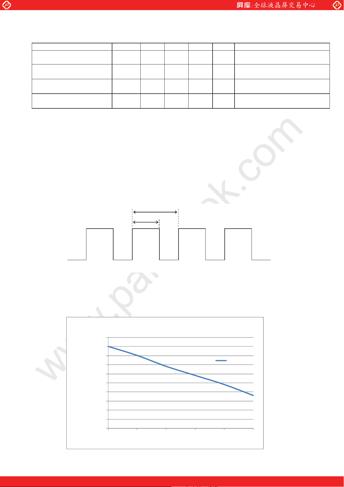
6.2. LED driving for back light
Parameter Symbol Min. Typ. Max. Unit Remark
LED Current ILED - 240 254.4 mA The value of each bar [Note 1]
LED Voltage VLED 88 97.8 110 V ILED =240mA [Note2]
www.panelook.com
LD-K23Z01-12
Ta=25Υ
PWM dimming frequency f
95 - 370 Hz
PWM
PWM dimming on duty PWM duty 0 - 100 % [Note 3]
[Note1] PIN1, PIN3,PIN5,PIN7 (CN101)
LED current (I
) is the value of each bar
LED
*Please decrease LED heat enough when the LED current is increased more than TYP value.
Please keep 85Υ or less the temperature of the terminal of LED.
[Note2] Ta = 25Υ, Measurement after 100ms has passed since power supply was turned on.
*The products are sensitive to the static electricity and care shall be fully taken when handling the products.
Particularly in case that an over-voltage which exceeds the Absolute Maximum Rating of the products shall be
applied, the overflowed energy may cause damages to, or possibly result in destruction of the products. Please take
absolutely secured countermeasures against static electricity and surge when handling the products.
1/ f
On time
PWM
V
F
Fig.1 LED Backlight PWM
[Note 3] Maximum allowed LED current against PWM duty is shown in below.
LED:Deratingcurve(DutyvsIf)
500
450
400
350
300
250
200
150
LEDcurrent:If(mA)
100
50
0
㻜 㻞㻜㻠㻜㻢㻜㻤㻜㻝㻜㻜
Duty(%)
One step solution for LCD / PDP / OLED panel application: Datasheet, inventory and accessory!
If(mA)
www.panelook.com
Page 15

Global LCD Panel Exchange Center
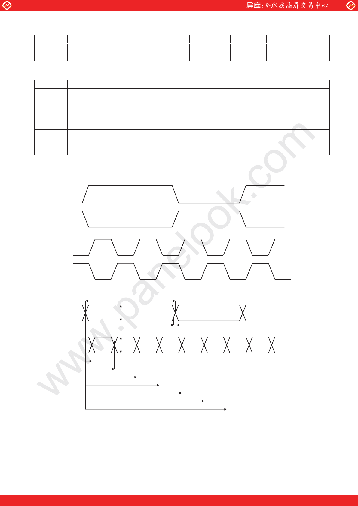
7 Timing characteristics of input signals
Timing characteristics
Timing diagrams of input signal are shown in Fig.2.
Parameter Symbol Min. Typ. Max. Unit Remark
www.panelook.com
LD-K23Z01-13
Clock Frequency 1/Tc 55
Horizontal period TH
Data enable
signal
Horizontal period
(High)
Vertical period TV
Vertical period
(High)
THd
TVd 1080 1080 1080 line
[Note]-When vertical period is very long, flicker and etc. may occur.
-Please turn off the module after it shows the black screen.
-Please make sure that length of vertical period should become of an integral multiple of horizontal
length of period. Otherwise, the screen may not display properly.
-As for your final setting of driving timing, we will conduct operation check test at our side, please
inform your final setting.
TH
DE
Aport DATA
1
5
(R,G,B)
Bport DATA
2
2
6
(R,G,B)
Cport DATA
3
7 1919 1919
(R,G,B)
Dport DATA
4
8 1920 1920
(R,G,B)
Tc
DE
TV
Fig.2 Timing characteristics of input signals
74.25
515
6.94
480
1120
73.052
THd
1 2 1080
550
7.41
480
1125
120
1917 1917
1918 1918
1079
TVd
80
825
11.1
480
1400
120.64
MHz
Clock
μs
Clock
Line
Hz
One step solution for LCD / PDP / OLED panel application: Datasheet, inventory and accessory!
www.panelook.com
Page 16
Global LCD Panel Exchange Center
LVDS DC Specifications
Symbol Parameter Condition Min. Typ. Max. units
Vod Differential voltage
VCM Common mode voltage
LVDS AC Specifications
Symbol Parameter Min. Typ. Max. units
tCLK LVDS clock period 13.15 13.47 16,67 ns
tpd0 LVDS data position 0 -0.25 0 +0.25 ns
tpd1 LVDS data position 1
tpd2 LVDS data position 2
tpd3 LVDS data position 3
tpd4 LVDS data position 4
tpd5 LVDS data position 5
tpd6 LVDS data position 6
LVDS DC & AC Specifications
www.panelook.com
LD-K23Z01-14
=100Ȑ
R
T
=100Ȑ
R
T
1/7tCLK-0.25 1/7tCLK 1/7tCLK
2/7tCLK-0.25 2/7tCLK 2/7tCLK
3/7tCLK-0.25 3/7tCLK 3/7tCLK
4/7tCLK-0.25 4/7tCLK 4/7tCLK
5/7tCLK-0.25 5/7tCLK 5/7tCLK
6/7tCLK-0.25 6/7tCLK 6/7tCLK
200 400 600 mV
1.0 1.2 1.4 V
ns
ns
ns
ns
ns
ns
Fig. 1
CLK_P
CLK_N
DATA_P
DATA_N
Fig. 2
CLK_N
CLK_P
DATA_N
DATA_P
Voc
Voc
Voc
Voc
Vod=0
Vod=0
tCLK
Vod
Vod
80%
20%
tLVT
tpd0
tpd1
tpd2
tpd3
tpd4
tpd5
tpd6
One step solution for LCD / PDP / OLED panel application: Datasheet, inventory and accessory!
www.panelook.com
Page 17
Global LCD Panel Exchange Center
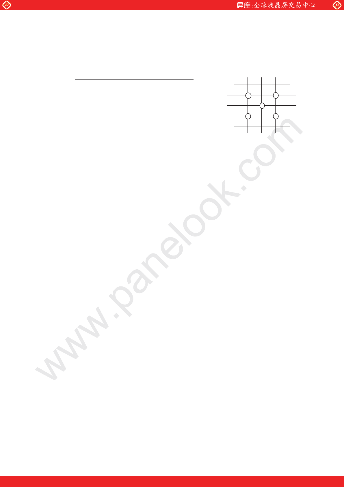
Input data signal and display position on the screen
R1G1B1R2G2B2
㸯㺂㸯 㸯㸰
R1G1B1R2G2B2
㸯㺂㸱 㸯㸲
www.panelook.com
LD-K23Z01-15
㸯࣭㸯㸯࣭㸰㸯࣭㸱
㸰࣭㸯㸰࣭㸰
㸱࣭㸯
㺃
㸯࣭㸲
RGB
Display position of Dat (V,H)
㺃
㺃
One step solution for LCD / PDP / OLED panel application: Datasheet, inventory and accessory!
www.panelook.com
Page 18

Global LCD Panel Exchange Center
8 Input Signal, Basic Display Colors and Gray Scale of Each Color
Colors &
Gray scale
Black – 0 0 0 0 0 0 0 0 0 0 0 0 0 0 0 0 0 0 0 0 0 0 0 0 0 0 0 0 0 0
Blue – 0 0 0 0 0 0 0 0 0 0 0 0 0 0 0 0 0 0 0 0 1 1 1 1 1 1 1 1 1 1
Green – 0 0 0 0 0 0 0 0 0 0 1 1 1 1 1 1 1 1 1 1 0 0 0 0 0 0 0 0 0 0
Cyan – 0 0 0 0 0 0 0 0 0 0 1 1 1 1 1 1 1 1 1 1 1 1 1 1 1 1 1 1 1 1
Red – 1 1 1 1 1 1 1 1 1 1 0 0 0 0 0 0 0 0 0 0 0 0 0 0 0 0 0 0 0 0
Basic Color
Magenta – 1 1 1 1 1 1 1 1 1 1 0 0 0 0 0 0 0 0 0 0 1 1 1 1 1 1 1 1 1 1
Yellow – 1 1 1 1 1 1 1 1 1 1 1 1 1 1 1 1 1 1 1 1 0 0 0 0 0 0 0 0 0 0
White – 1 1 1 1 1 1 1 1 1 1 1 1 1 1 1 1 1 1 1 1 1 1 1 1 1 1 1 1 1 1
Black GS0 0 0 0 0 0 0 0 0 0 0 0 0 0 0 0 0 0 0 0 0 0 0 0 0 0 0 0 0 0 0
Darker GS2 0 1 0 0 0 0 0 0 0 0 0 0 0 0 0 0 0 0 0 0 0 0 0 0 0 0 0 0 0 0
Brighter GS1021 1 0 1 1 1 1 1 1 1 1 0 0 0 0 0 0 0 0 0 0 0 0 0 0 0 0 0 0 0 0
Gray Scale of Red
Gray
R0 R1 R2 R3 R4 R5 R6 R7 R8 R9 G0 G1 G2 G3 G4 G5 G6 G7 G8 G9 B0 B1 B2 B3 B4 B5 B6 B7 B8 B9
Scale
× GS1 1 0 0 0 0 0 0 0 0 0 0 0 0 0 0 0 0 0 0 0 0 0 0 0 0 0 0 0 0 0
×
Ø
p
p
Ø GS1022 0 1 1 1 1 1 1 1 1 1 0 0 0 0 0 0 0 0 0 0 0 0 0 0 0 0 0 0 0 0
www.panelook.com
LD-K23Z01-16
Data signal
p
p
p
p
p
p
Red GS1023 1 1 1 1 1 1 1 1 1 1 0 0 0 0 0 0 0 0 0 0 0 0 0 0 0 0 0 0 0 0
Black GS0 0 0 0 0 0 0 0 0 0 0 0 0 0 0 0 0 0 0 0 0 0 0 0 0 0 0 0 0 0 0
× GS1 0 0 0 0 0 0 0 0 0 0 1 0 0 0 0 0 0 0 0 0 0 0 0 0 0 0 0 0 0 0
Darker GS2 0 0 0 0 0 0 0 0 0 0 0 1 0 0 0 0 0 0 0 0 0 0 0 0 0 0 0 0 0 0
×
Ø
Brighter GS1021 0 0 0 0 0 0 0 0 0 0 1 0 1 1 1 1 1 1 1 1 0 0 0 0 0 0 0 0 0 0
Gray Scale of Green
Ø GS1022 0 0 0 0 0 0 0 0 0 0 0 1 1 1 1 1 1 1 1 1 0 0 0 0 0 0 0 0 0 0
Green GS1023 0 0 0 0 0 0 0 0 0 0 1 1 1 1 1 1 1 1 1 1 0 0 0 0 0 0 0 0 0 0
Black GS0 0 0 0 0 0 0 0 0 0 0 0 0 0 0 0 0 0 0 0 0 0 0 0 0 0 0 0 0 0 0
p
p
p
p
p
p
p
p
× GS1 0 0 0 0 0 0 0 0 0 0 0 0 0 0 0 0 0 0 0 0 1 0 0 0 0 0 0 0 0 0
Darker GS2 0 0 0 0 0 0 0 0 0 0 0 0 0 0 0 0 0 0 0 0 0 1 0 0 0 0 0 0 0 0
Ø
Ø
Brighter GS1021 0 0 0 0 0 0 0 0 0 0 0 0 0 0 0 0 0 0 0 0 1 0 1 1 1 1 1 1 1 1
Gray Scale of Blue
Ø GS1022 0 0 0 0 0 0 0 0 0 0 0 0 0 0 0 0 0 0 0 0 0 1 1 1 1 1 1 1 1 1
Blue GS1023 0 0 0 0 0 0 0 0 0 0 0 0 0 0 0 0 0 0 0 0 1 1 1 1 1 1 1 1 1 1
p
p
p
p
p
p
p
p
0: Low level voltage, 1: High level voltage.
Each basic color can be displayed in 1024 gray scales from 10 bits data signals. According to the combination of
total 30 bits data signals, one billion-color display can be achieved on the screen.
One step solution for LCD / PDP / OLED panel application: Datasheet, inventory and accessory!
www.panelook.com
Page 19
Global LCD Panel Exchange Center
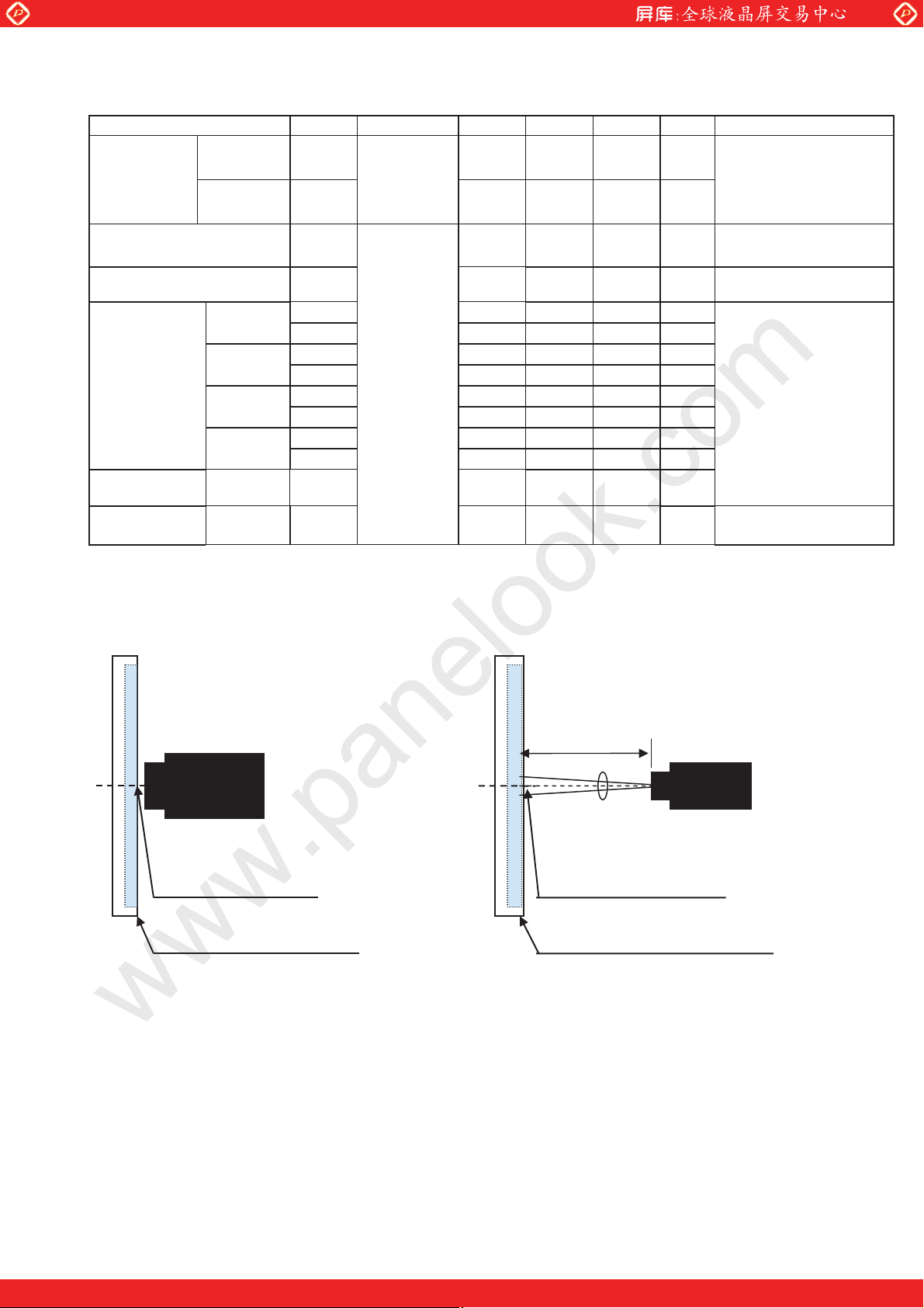
9 Optical characteristics
Parameter Symbol Condition Min. Typ. Max. Unit Remark
Horizontal
Viewing angle
range
Vertical
T
T
T
T
21
22
11
12
www.panelook.com
LD-K23Z01-17
Ta=25qC, Vcc=12.0V, VLED =(97.8)V , frame rate:120Hz (typ.value)
CRӍ10
70 88 - Deg.
70 88 -
Deg.
[Note1,4]
Contrast ratio CRn
Response time
White
Red
Chromaticity
Green
Blue
Luminance White YL 350 400 - cd/m2
Luminance
uniformity
Measurement condition
*The measurement shall be executed 60 minutes after lighting at rating.
[Note]The optical characteristics are measured using the following equipment.
Detector㸦EZ-CONTRAST/ Photodiode㸧
Middle of the screen (T㸻0q)
TFT-LCD Module
Fig.4-1 Measurement of viewing angle range and
Response time.
White
Viewing angle range: EZ-CONTRAST
Response time: Photodiode
W
DRV
x 0.250 0.280 0.310 y 0.249 0.279 0.309 x 0.612 0.642 0.672 y 0.323 0.353 0.383 x 0.284 0.314 0.344 y 0.615 0.645 0.675 x 0.126 0.156 0.186 y 0.022 0.052 0.082 -
Gw
T
=0 deg.
3750 5000 - [Note2,4]
- 6 8 ms [Note3,4,5]
1.25 [Note 6]
Detector㸦SR-3㸧
400mm
Field=1q
Middle of the screen (T㸻0q)
TFT-LCD Module
Fig.4-2 Measurement of Contrast, Luminance,
Chromaticity.
I
LED
=0.240A
[Note4]
One step solution for LCD / PDP / OLED panel application: Datasheet, inventory and accessory!
www.panelook.com
Page 20

Global LCD Panel Exchange Center
[Note 1]Definitions of viewing angle range :
T
22
T
12
[Note 2]Definition of contrast ratio :
The contrast ratio is defined as the following.
Luminance (brightness) with all pixels white
Contrast Ratio
Luminance (brightness) with all pixels black
[Note 3]Definition of response time
The response time (T
)) is defined as the following figure and shall be measured by switching the input
DRV
signal for “any level of gray (0%, 25%, 50%, 75% and 100%)” and “any level of gray (0%, 25%, 50%, 75%
and 100%)”.
www.panelook.com
Normal line
T
11
6 o’clock direction
㸻
T
LD-K23Z01-18
21
0%
0%
25㸣
50㸣
75㸣
100%
td: 25%-0㸣
td: 50%-0㸣 td: 50%-25㸣
td: 75%-0㸣 td: 75%-25㸣 td: 75%-50㸣
td: 100%-0㸣 td: 100%-25㸣 td: 100%-50㸣 td:100%-75㸣
25㸣 50㸣 75㸣
tr:0%-25㸣
tr:0%-50% tr:0%-75% tr:0%-100%
tr: 25%-50㸣 tr25%-75㸣 tr: 25%-100㸣
tr: 50%-75㸣 tr: 50%-100㸣
100%
tr: 75%-100㸣
t*:x-y...response time from level of gray(x) to level of gray(y)
W
= 6(t*:x-y)/20
DRV
any level of gray
(bright)
100%
90%
any level of gray
(dark)
any level of gray
(bright)
Photodetector
10%
Output
0%
td:* tr:*
time
[Note 4]This shall be measured at center of the screen.
[Note 5] This value is valid when O/S driving is used at typical input time value.
One step solution for LCD / PDP / OLED panel application: Datasheet, inventory and accessory!
www.panelook.com
Page 21
Global LCD Panel Exchange Center
10.1. Fail safe design
10.2. Handling Precautions of the module
[Note 6]Definition of white uniformity ;
White uniformity is defined as the following with five measurements. (AaE)
Maximum luminance of five points (brightness)
㹕㸻
G
Minimum luminance of five points (brightness)
10 Precautions
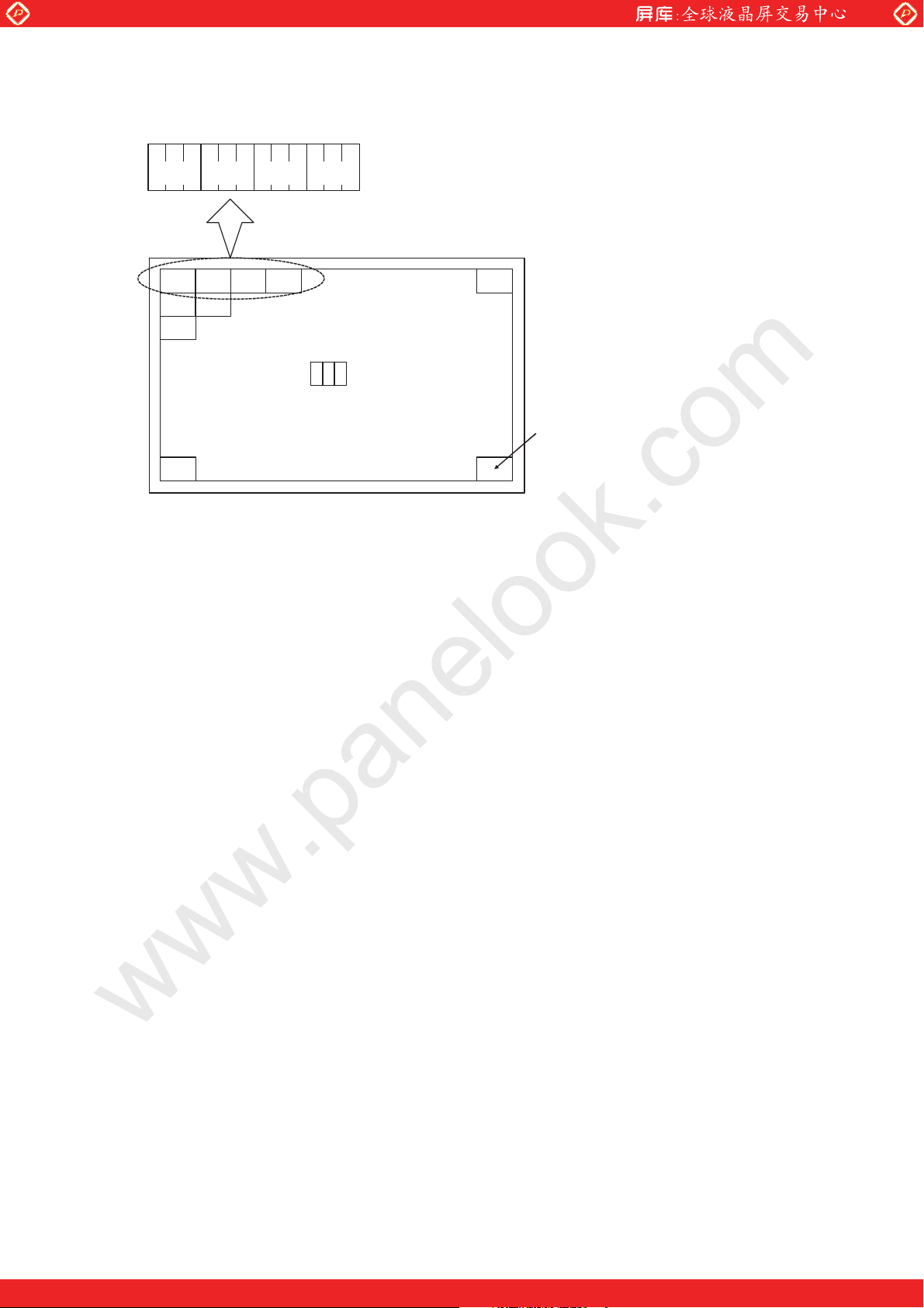
LCD Module has an inherent chance of failure. Customers must protect against injury, damage or
less from such failures by incorporating safety design measures into your facility and equipment
such as redundancy, fire protection, and prevention of over-current levels and other abnormal
operating conditions.
a) Be sure to turn off the power supply when inserting or disconnecting the cable.
b) Be sure to design the cabinet so that the module can be installed without any extra stress such as warp or
twist.
c) Since the front polarizer is easily damaged, pay attention not to scratch it.
d) Since long contact with water may cause discoloration or spots, wipe off water drop immediately.
e) When the panel surface is soiled, wipe it with absorbent cotton or other soft cloth.
f) Since the panel is made of glass, it may break or crack if dropped or bumped on hard surface. Handle with
care.
g) Since CMOS LSI is used in this module, take care of static electricity and take the human earth into
consideration when handling.
h) The module has some printed circuit boards (PCBs) on the back side, take care to keep them form any stress
or pressure when handling or installing the module; otherwise some of electronic parts on the PCBs may be
damaged.
i) Observe all other precautionary requirements in handling components.
j) When some pressure is added onto the module from rear side constantly, it causes display non-uniformity
issue, functional defect, etc. So, please avoid such design.
k) When giving a touch to the panel at power on supply, it may cause some kinds of degradation. In that case,
once turn off the power supply, and turn on after several seconds again, and that is disappear.
l) When handling LCD modules and assembling them into cabinets, please be noted that long-term storage in
the environment of oxidization or deoxidization gas and the use of such materials as reagent, solvent,
adhesive, resin, etc. which generate these gasses, may cause corrosion and discoloration of the LCD
modules.
m) This LCD module is designed to prevent dust from entering into it. However, there would be a possibility to
have a bad effect on display performance in case of having dust inside of LCD module. Therefore,
please ensure to design your TV set to keep dust away around LCD module.
www.panelook.com
480
960 1440
A㻌
C㻌
B㻌
LD-K23Z01-19
pixel
D㻌
E㻌
270
540
810
pixel
㻌
One step solution for LCD / PDP / OLED panel application: Datasheet, inventory and accessory!
www.panelook.com
Page 22

Global LCD Panel Exchange Center
2
11 Packing form
a) Piling number of cartons : 4
b) Packing quantity in one carton : 18pcs
c) Carton size : 1115(W)1090(D)790(H)mm
d) Total mass of one carton filled with full modules : 165kg
12 Reliability test item
No. Test item Condition
1
2
3
4
5
6
7
8
[Result evaluation criteria]
Under the display quality test condition with normal operation state, there shall be no change, which may
affect practical display function.
*For Shock test and Vibration test, the method of fixation is not guaranteed excluding the method
written in the attached document: ” The reliability test form (shock test & vibration test)”
High temperature storage test
Low temperature storage test
High temperature and high humidity
operation test
High temperature operation test
Low temperature operation test
Vibration test
(non-operation)
Shock test
(non-operation)
ESD
www.panelook.com
Ta=60qC 240h
Ta=-25qC240h
Ta=40qC ; 95%RH 240h
(No condensation)
Ta=50qC 240h
Ta=0qC 240h
Frequency: 10~57Hz/Vibration width (one side): 0.075mm
: 58~500Hz/Acceleration: 9.8 m/s²
Sweep time: 11 minutes
Test period: 3 hours (1h for each direction of X, Y, Z)
Maximum acceleration: (294m/s
Pulse width: 11ms, sinusoidal half wave
Direction: +/-X, +/-Y, +/-Z, once for each direction.
* At the following conditions, it is a thing without incorrect
operation and destruction.
(1)Non-operation: Contact electric discharge r10kV
(2)Operation Contact electric discharge r8kV
Conditions: 150pF, 330ohm
LD-K23Z01-20
)
Non-contact electric discharge r20kV
Non-contact electric discharge r15kV
One step solution for LCD / PDP / OLED panel application: Datasheet, inventory and accessory!
www.panelook.com
Page 23

Global LCD Panel Exchange Center
㸦
㸲㹑
㸧
LK400D3LC03(*)
㸦㹏㸧
13 Others
The label that displays SHARP, product model (LK400D3LC03), a product number is stuck on the back of the
module.
࠙LK400D3LC03ࠚ
No Item Remark
SHARP Logo mark Siz e: 16. 0 mm x 2.0 mm
䐟
2D Barcode (
䐠
model name (including the management character)
Model name
䐡
Barcode (
䐢
module Lot number “յ” *11P00001*
Module Lot number
䐣
(SHARP module serial)
Barcode (
䐤
12NC and seral No. (The last 8 digiits of 12NC) (䐣Module lot No.
12NC (Philips code)
䐥
2) Packing Label
[LK400D3LC03]
02'(/㸸
Bar code
㹊㹭㹲㹌㹍㸬
Bar code
㹏㹳㹟㹬㹲㹧㹲㹷㸸
Bar code
&8670(502'(/
Bar code
3) Adjusting volume has been set optimally before shipment, so do not change any adjusted value.
If adjusted value is changed, the specification may not be satisfied.
4) Disassembling the module can cause permanent damage and should be strictly avoided.
5) Please be careful since image retention may occur when a fixed pattern is displayed for a long time.
6) The chemical compound, which causes the destruction of ozone layer, is not being used.
7) When any question or issue occurs, it shall be solved by mutual discussion.
8) This module is corresponded to RoHS.
ECC200
CODE39
CODE128
) Module Lot number
㸦㸯㹒㸧㸰㸮㸯㸯㸨㸨㸨ղ
www.panelook.com
) In-company model name ( LK400D3LB53J )
External model name
Font: Arial Size: 8
P 0 0 0 0 1
21
(Year & Month) (Factory) (Serial No.)
Font: Arial Size: 7
) YYYY ZZZZ
ձ
㹮㹡㹱ճ
;;;;;;;;;;;;մ
11P00001
XXXX Y Y Y Y ZZZZ
Font: Arial Size: 7
ձ Management No :
ղ Lot No. (Date)
ճ Quantity
մ User code
LD-K23Z01-21
䠅
One step solution for LCD / PDP / OLED panel application: Datasheet, inventory and accessory!
www.panelook.com
Page 24

Global LCD Panel Exchange Center
14 Carton storage condition
Temperature 0qC to 40qC
Humidity 95%RH or less
Reference condition : 20qC to 35qC, 85%RH or less (summer)
: 5qC to 15qC, 85%RH or less (winter)
the total storage time (40qC,95%RH) : 240H or less
Sunlight Be sure to shelter a product from the direct sunlight.
Atmosphere Harmful gas, such as acid and alkali which bites electronic components and/or
wires must not be detected.
Notes Be sure to put cartons on palette or base, don’t put it on floor, and store them with
removing from wall
Please take care of ventilation in storehouse and around cartons, and control
changing temperature is within limits of natural environment
Storage life 1 year
www.panelook.com
LD-K23Z01-22
One step solution for LCD / PDP / OLED panel application: Datasheet, inventory and accessory!
www.panelook.com
Page 25
Global LCD Panel Exchange Center
www.panelook.com
One step solution for LCD / PDP / OLED panel application: Datasheet, inventory and accessory!
www.panelook.com
Page 26

Global LCD Panel Exchange Center
www.panelook.com
One step solution for LCD / PDP / OLED panel application: Datasheet, inventory and accessory!
www.panelook.com
 Loading...