

Page 1
Global LCD Panel Exchange Center
www.panelook.com
TECHNICAL LITERATURE
TFT - LCD PANEL
( Open Cell )
㨀㧱㧺㨀㧭㨀㧵㨂㧱
FOR
No.
DATE May. 21. 2010
LD-K22553
MODEL No.
The technical literature is subject to change without notice.
So, please contact SHARP or its representative before designing
your product based on this literature.
LK400D3HA
㧖㧖
DEVELOPMENT DEPARTMENT. 2
LIQUID CRYSTAL DISPLAY DIVISION.1
LIQUID CRYSTAL DISPLAY GROUP
SHARP CORPORATION
One step solution for LCD / PDP / OLED panel application: Datasheet, inventory and accessory!
www.panelook.com
Page 2
Global LCD Panel Exchange Center
RECORDS OF REVISION
LK400D3HA㧖㧖
www.panelook.com
SPEC No. DATE
No. PAGE
LD-K22553 May. 21. 2010 - - - 1st. Issue
REVISED
SUMMARY NOTE
One step solution for LCD / PDP / OLED panel application: Datasheet, inventory and accessory!
www.panelook.com
Page 3
Global LCD Panel Exchange Center
1 Application
This specification applies to the color 40.0” TFT-LCD Open Cell LK400D3HA㧖㧖
With parts (FPC,C-PWB) to drive it.䯵
䯴
* These specification are proprietary products of SHARP CORPORATION (“SHARP”) and include materials
protected under copyright of SHARP. Do not reproduce or cause any third party to reproduce them in any form or
by any means, electronic or mechanical, for any purpose, in whole or in part, without the express written
permission of SHARP.
* In case of using the device for applications such as control and safety equipment for transportation (aircraft, trains,
automobiles, etc.), rescue and security equipment and various safety related equipment which require higher
reliability and safety, take into consideration that appropriate measures such as fail-safe functions and redundant
system design should be taken.
* Do not use the device for equipment that requires an extreme level of reliability, such as aerospace applications,
telecommunication equipment (trunk lines), nuclear power control equipment and medical or other equipment for
life support.
* SHARP assumes no responsibility for any damage resulting from the use of the device that does not comply with
the instructions and the precautions specified in these specification.
* Contact and consult with a SHARP sales representative for any questions about this device.
2 Overview
This Open Cell is a color active matrix LCD Open-Cell incorporating amorphous silicon TFT (Thin Film Transistor).
It is composed of a color TFT-LCD panel, driver ICs and Source PWB. The following content can be achieved in
using LK0DZ1C0㧖㧖㧖(CONTROL PWBC-PWB) and LK0DZ1C0112 (FPC) that SHARP specifies. Graphics
and texts can be displayed on a 1920RGB1080 dots panel with one billion colors by using 10bit+ LVDS (L
V
oltage Differential Signaling) to interface, +12V of DC supply voltages.Graphics and texts can be displayed on a
1920RGB1080 dots panel with one billion colors by using 10bit+ LVDS (L
interface, +12V of DC supply voltages.
And in order to improve the response time of LCD, This C-PWB applies the Over Shoot driving (O/S driving)
technology for the control circuit .In the O/S driving technology, signals are being applied to the Liquid Crystal
according to a pre-fixed process as an image signal of the present frame when a difference is found between image
signal of the previous frame and that of the current frame after comparing them.
With combination of these technologies, motion blur can be reduced and clearer display performance can be realized.
www.panelook.com
LD-K22553䙱1
ow
ow Voltage Differential Signaling) to
LK0DZ1C0㧖㧖㧖
LK0DZ1C0112
CN1
CONTROL PWB
Control Signals
FPC
SOURCE PWB
SOURCE DRIVER
GATE DRIVER
LCD PANEL
1920×3(RGB)×1080
LK400D3HA㧖㧖 (Open Cell)
CN2
CN3
Power Supply
Circuit
FPC
GATE DRIVER
One step solution for LCD / PDP / OLED panel application: Datasheet, inventory and accessory!
www.panelook.com
Page 4
Global LCD Panel Exchange Center
3 Mechanical Specifications
Parameter Specifications Unit
Display size
Active area 885.6H) x 498.15 (V) mm
Pixel Format
Pixel pitch 461.25(H) x 461.25 (V) um
Pixel configuration R, G, B vertical stripe
Display mode Normally black
Cell Outline Dimensions[Note1] 921.18(H) x 548.55(V) x 1.82(D) mm
Mass
Surface treatment [Note2]
(Upper Polarizing film)
Surface treatment [Note2]
(Lower Polarizing film)
[Note1] Outline dimensions are shown in P21.
[Note2] With the protection film removed.
www.panelook.com
101.609 㧔Diagonal㧕
40.0 㧔Diagonal㧕
1920(H) x 1080(V)
㧔1pixel = R + G + B dot㧕
1.81 r0.3
Low-Haze Anti Glare
Hard coating : 2H and more
Plane
Hard coating :㧙
LD-K22553䙱2
cm
inch
pixel
kg
One step solution for LCD / PDP / OLED panel application: Datasheet, inventory and accessory!
www.panelook.com
Page 5
Global LCD Panel Exchange Center
y
q
)
q
)
q
)
q
]
(
)
p
r
[
]
q
)
)
q
)
)
q
)
)
p
p
p
p
p
p
K
)
p
)
p
p
p
p
p
p
p
p
p
p
K
)
p
)
p
p
p
p
pply
pply
pply
pply
pply
4 Cell Driving Specifications
www.panelook.com
LD-K22553䙱3
4.1
Driving interface of Control PWB SHARP specifies[
CN1 (Interface signals and +12V DC power supply)
Using connector : FI-RNE51SZ-HF (Japan Aviation Electronics Ind., Ltd.)
Matching connector : FI-RE51HL, FI-RE51CL (Japan Aviation Electronics Ind., Ltd.)
Matching LVDS transmitter : THC63LVD1023 or equivalent device
Pin No. S
1
2
3
4
5
6
7
8
9
10
11 GND
12
13
14
15
16
17
18
19
20
21
22
23
24
25
26
27
28
29
30
31
32
33
34
35
36
37
38
39
40
41
42
43
44
45
46
47
48
49
50
51
mbol Function Remark
GND
Reserved It is re
Reserved It is re
Reserved It is re
FRAME
O/S set O/S o
SELLVDS
Reserved
Reserved
Reserved
AIN0- A
AIN0+ A
AIN1- A
AIN1+ A
AIN2- A
AIN2+ A
GND
AC
ACK+ A
GND
AIN3- A
AIN3+ A
AIN4- A
AIN4+ A
GND
GND
BIN0- B
BIN0+ B
BIN1- B
BIN1+ B
BIN2- B
BIN2+ B
GND
BC
BCK+ B
GND
BIN3- B
BIN3+ B
BIN4- B
BIN4+ B
GND
GND
GND
GND
GND
VCC +12V Power Su
VCC +12V Power Su
VCC +12V Power Su
VCC +12V Power Su
VCC +12V Power Su
Frame fre
Select LVDS data orde
It is re
It is re
It is re
- Aport LVDS Clock signal(-
- Bport LVDS Clock signal(-
uired to set non-connection(OPEN
uired to set non-connection(OPEN
uired to set non-connection(OPEN
uency setting 0:120Hz 1:100Hz[Note 1
eration setting H:O/S ON, L:O/S OFF [Note 2] Pull up 3.3V
uired to set non-connection(OPEN
uired to set non-connection(OPEN
uired to set non-connection(OPEN
ort (-)LVDS CH0 differential data input
ort (+)LVDS CH0 differential data input
ort (-)LVDS CH1 differential data input
ort (+)LVDS CH1 differential data input
ort (-)LVDS CH2 differential data input
ort (+)LVDS CH2 differential data input
ort LVDS Clock signal(+
ort (-)LVDS CH3 differential data input
ort (+)LVDS CH3 differential data input
ort (-)LVDS CH4 differential data input
ort (+)LVDS CH4 differential data input
(Shown in Fig1)
Note 2,3
LK0DZ1C0
㧖㧖㧖]
Pull up 3.3V
Pull up 3.3V
Pull up 3.3V
Pull down :
Pull up 3.3V
Pull down : (GND
Pull down : (GND
Pull down : (GND
GND
One step solution for LCD / PDP / OLED panel application: Datasheet, inventory and accessory!
www.panelook.com
Page 6
Global LCD Panel Exchange Center
(
y)
(
y)
(
y)
p
p
p
p
p
p
K
)
p
)
p
p
p
p
p
p
p
p
p
p
K
)
p
)
p
p
p
p
CN2 (Interface signals) (Shown in Fig1)
Using connector : FI-RNE41SZ-HF (Japan Aviation Electronics Ind., Ltd.)
Matching connector : FI-RE41HL, FI-RE41CL (Japan Aviation Electronics Ind., Ltd.)
Pin No. Symbol Function Remark
1
2
3
4
5
Reserved
Reserved
Reserved
VCC) (+12V Power Suppl
VCC) (+12V Power Suppl
VCC) (+12V Power Suppl
Reserved
Reserved
6 Reserved
7 Reserved
8 Reserved
9 GND
10
11
12
13
14
15
16
17
18
19
20
21
22
23
24
25
26
27
28
29
30
31
32
33
34
35
36
37
38
39
40
41
CIN0- C
CIN0+ C
CIN1- C
CIN1+ C
CIN2- C
CIN2+ C
GND
CC
- Cport LVDS Clock signal(-
CCK+ C
GND
CIN3- C
CIN3+ C
CIN4- C
CIN4+ C
GND
GND
DIN0- D
DIN0+ D
DIN1- D
DIN1+ D
DIN2- D
DIN2+ D
GND
DC
- Dport LVDS Clock signal(-
DCK+ D
GND
DIN3- D
DIN3+ D
DIN4- D
DIN4+ D
GND
GND
[Note] GND of parts drived a liquid crystal panel drive has connected with a module chassis.
[Note 1]The equivalent circuit figure of the terminal
Control PWB
www.panelook.com
LD-K22553䙱4
ort (-)LVDS CH0 differential data input
ort (+)LVDS CH0 differential data input
ort (-)LVDS CH1 differential data input
ort (+)LVDS CH1 differential data input
ort (-)LVDS CH2 differential data input
ort (+)LVDS CH2 differential data input
ort LVDS Clock signal(+
ort (-)LVDS CH3 differential data input
ort (+)LVDS CH3 differential data input
ort (-)LVDS CH4 differential data input
ort (+)LVDS CH4 differential data input
100
Te rm in al
2.0K
One step solution for LCD / PDP / OLED panel application: Datasheet, inventory and accessory!
www.panelook.com
Page 7

Global LCD Panel Exchange Center
V
[Note 2]The equivalent circuit figure of the terminal
100
Te rm in al
www.panelook.com
LD-K22553䙱5
3.3
2.0K
[Note 3] LVDS Data order
Data L(GND)
TA0
TA1
TA2
TA3
TA4
TA5
TA6
TB0
TB1
TB2
TB3
TB4
TB5
TB6
TC0
TC1
TC2
TC3
TC4 NA NA
TC5 NA NA
TC6 DE(*) DE(*)
TD0
TD1
TD2
TD3
TD4
TD5
TD6
TE0
TE1
TE2
TE3
TE4
TE5
TE6
NA: Not Available
(*)Since the display position is prescribed by the rise of DE(Display Enable)signal, please do not fix DE
signal during operation at ”High”.
SELLVDS
[VESA]
R0(LSB)㩷
R1㩷
R2㩷
R3㩷
R4㩷
R5㩷
G0(LSB)㩷
G1㩷
G2㩷
G3㩷
G4㩷
G5㩷
B0(LSB)㩷
B1㩷
B2㩷
B3㩷
B4㩷
B5㩷
R6㩷
R7㩷
G6㩷
G7㩷
B6㩷
B7㩷
N/A㩷
R8㩷
R9(MSB)㩷
G8㩷
G9(MSB)㩷
B8㩷
B9(MSB)㩷
N/A㩷
H(3.3V) or Open
[JEIDA]
R4
R5
R6
R7
R8
R9(MSB)
G4
G5
G6
G7
G8
G9(MSB)
B4
B5
B6
B7
B8
B9(MSB)
R2
R3
G2
G3
B2
B3
N/A
R0(LSB)
R1
G0(LSB)
G1
B0(LSB)
B1
N/A
Control PWB
One step solution for LCD / PDP / OLED panel application: Datasheet, inventory and accessory!
www.panelook.com
Page 8
Global LCD Panel Exchange Center
–
,
–
–
,
–
SELLVDS= Low (GND)
ACK+,BCK+
CCK+,DCK+
ACK– ,BCK–
CCK– ,DCK–
AIN0+,BIN0+
CIN0+,DIN0+
AIN0
–,BIN0–
CIN0–,DIN0–
AIN1+,BIN1+
CIN1+,DIN1+
AIN1
–,BIN1–
CIN1–,DIN1–
AIN2+,BIN2+
CIN2+,DIN2+
AIN2
–,BIN2–
CIN2–,DIN2–
AIN3+,BIN3+
CIN3+,DIN3+
AIN3
–,BIN3–
CIN3–,DIN3–
AIN4+,BIN4+
CIN4+,DIN4+
AIN4
–,BIN4–
CIN4
DIN4
www.panelook.com
LD-K22553䙱6
1 cycle
G0 R5 R4 R3 R2 R1 R0 R0 R1 G0
B1 B0 G5 G4 G3 G2 G1 G1 G2 B1
DE
NA NA
B7 B6 G7 G6 R7 R6 R6 R7 NA NA
B9 B8 G9 G8 R9 R8 R8 R9 NA NA
B5 B4 B3 B2 B2 B3
DE
SELLVDS= High (3.3V) or OPEN
ACK+,BCK+
CCK+,DCK+
ACK– ,BCK–
CCK– ,DCK–
AIN0+,BIN0+
CIN0+,DIN0+
AIN0–,BIN0–
CIN0–,DIN0–
AIN1+,BIN1+
CIN1+,DIN1+
AIN1
CIN1–,DIN1–
AIN2+,BIN2+
CIN2+,DIN2+
–,BIN2–
AIN2
CIN2–,DIN2–
AIN3+,BIN3+
CIN3+,DIN3+
AIN3
CIN3–,DIN3–
AIN4+,BIN4+
CIN4+,DIN4+
–,BIN4–
AIN4
CIN4
–,BIN1–
–,BIN3–
DIN4
DE: Display Enable, NA: Not Available (Fixed Low)
1 cycle
G4 R9 R8 R7 R6 R5 R4 R4 R5 G4
B5 B4 G9 G8 G7 G6 G5 G5 G6 B5
DE
NA NA
B3 B2 G3 G2 R3 R2 R2 R3 NA NA
B1 B0 G1 G0 R1 R0 R0 R1 NA NA
B9 B8 B7 B6 B6 B7
DE
One step solution for LCD / PDP / OLED panel application: Datasheet, inventory and accessory!
www.panelook.com
Page 9

Global LCD Panel Exchange Center
㪠㪥㪧㪬㪫㩷㪪㪠㪞㪥㪘㪣㪪㩷
㪧㪦㪮㪜㪩㩷㪪㪬㪧㪧㪣㪰
㩷
㪣㪚㪛㩷㪧㪘㪥㪜㪣㩷
㪈㪐㪉㪇㬍㪊㩿㪩㪞㪙㪀㬍㪈㪇㪏㪇㩷
㪞㪘㪫㪜㩷㪛㪩㪠㪭㪜㪩㩷
㪞㪘㪫㪜㩷㪛㪩㪠㪭㪜㪩㩷
㪠㪥㪧㪬㪫㩷㪪㪠㪞㪥㪘㪣㪪㩷
㪚㪄㪧㪮㪙㩷
㪪㪦㪬㪩㪚㪜 㪛㪩㪠㪭㪜㪩
㪪㪦㪬㪩㪚㪜 㪧㪮㪙
Interface block diagram
㪚㪠㪥㪇㪄㩷㪚㪠㪥㪇㪂㩷
㪚㪠㪥㪈㪄㩷㪚㪠㪥㪈㪂㩷
㪚㪠㪥㪉㪄㩷㪚㪠㪥㪉㪂㩷
㪚㪠㪥㪊㪄㩷㪚㪠㪥㪊㪂㩷
㪚㪠㪥㪋㪄㩷㪚㪠㪥㪋㪂㩷
㪚㪚㪢㪄㩷㪚㪚㪢㪂㩷
㪛㪠㪥㪇㪄㩷㪛㪠㪥㪇㪂㩷
㪛㪠㪥㪈㪄㩷㪛㪠㪥㪈㪂㩷
㪛㪠㪥㪉㪄㩷㪛㪠㪥㪉㪂㩷
㪛㪠㪥㪊㪄㩷㪛㪠㪥㪊㪂㩷
㪛㪠㪥㪋㪄㩷㪛㪠㪥㪋㪂㩷
㪛㪚㪢㪄㩷㪛㪚㪢㪂㩷
㩷
www.panelook.com
㩷
㪚㪥㪉㩷
2
㩷
㪚㫆㫅㫋㫉㫆㫃㩷
㪪㫀㪾㫅㪸㫃㫊
Fig.1
Interface block diagram
㪚㪥㪈㩷
㪧㫆㫎㪼㫉㩷㪪㫌㫇㫇㫃㫐
㪚㫀㫉㪺㫌㫀㫋㩷
㪝㫉㪸㫄㪼㩷
㪦㪆㪪㪶㫊㪼㫋㩷
㪪㪜㪣㪣㪭㪛㪪㩷 㩷
㪘㪠㪥㪇㪄㩷㪘㪠㪥㪇㪂㩷
㪘㪠㪥㪈㪄㩷㪘㪠㪥㪈㪂㩷
㪘㪠㪥㪉㪄㩷㪘㪠㪥㪉㪂㩷
㪘㪠㪥㪊㪄㩷㪘㪠㪥㪊㪂㩷
㪘㪠㪥㪋㪄㩷㪘㪠㪥㪋㪂㩷
㪘㪚㪢㪄㩷㪘㪚㪢㪂㩷
㪙㪠㪥㪇㪄㩷㪙㪠㪥㪇㪂㩷
㪙㪠㪥㪈㪄㩷㪙㪠㪥㪈㪂㩷
㪙㪠㪥㪉㪄㩷㪙㪠㪥㪉㪂㩷
㪙㪠㪥㪊㪄㩷㪙㪠㪥㪊㪂㩷
㪙㪠㪥㪋㪄㩷㪙㪠㪥㪋㪂㩷
㪙㪚㪢㪄㩷㪙㪚㪢㪂㩷
㩷
㩷 㩷 㪂㪈㪉㪭㩷㪛㪚㩷
LD-K22553䙱7
One step solution for LCD / PDP / OLED panel application: Datasheet, inventory and accessory!
www.panelook.com
Page 10
Global LCD Panel Exchange Center
㧖㧖㧖
4.2 Vcom Adjusting interface of Control PWB SHARP specifies[LK0DZ1C0
CN2(Interface Vcom Adjusting)
Using Via Hole : 1.5mm Pitch (Ǿ0.7mm )
Mating connector : (housing)3P-SZN, (contact)SZN-002T-P0.7K (JST Co.,Ltd.)
Communication method:
Pin No. Symbol Function Remark
1 SDA
I2C DATA
2 SCL I2C CLK Pull up 3.3V[Note2]
3 GND
Refer to specifications of ISL24837 for the I2C command of Vcom adjustment.
[Note1]Interface
PinNo Symbol
1 SDA
2 SCL
3 GND
[note1]
I2C
www.panelook.com
Pull up 3.3V[Note2]
[Note2] The equivalent circuit figure of the terminal
3.3[V]
3.3[V]
10[Kohm]
10[Kohm]
LD-K22553䙱8
]
Terminal
TerminalTerminal
4.3 Absolute Maximum Ratings
Parameter Symbol Condition Ratings Unit Remark
Input voltage
(for Control)
12V supply voltage
(for Control)
Storage temperature Tstg - -25 ~ +60
Operation temperature
(Ambient)
I
V
VCC
Ta=25 qC
Ta=25 qC
-0.3 ~ 3.6 V [Note 1]
0 ~ + 14 V
Topa - 0 ~ +50
qC
qC
[Note 2]
[Note 3]
[Note 1] SELLVDS FRAME, O/S_set,
[Note 2] Humidity 95%RH Max.(Ta҇40qC)
Maximum wet-bulb temperature at 39 qC or less.(Ta>40qC)
No condensation.
[Note 3] Because the operation temperature of IC200 is MAX 105, thermally conductive interface Pad is
recommended.
Refer to C-PWB specifications for IC200.
One step solution for LCD / PDP / OLED panel application: Datasheet, inventory and accessory!
www.panelook.com
Page 11

Global LCD Panel Exchange Center
4.4 Electrical Characteristics of input signals
Parameter Symbol Min. Typ. Max. Unit Remark
Supply voltage Vcc 11.4 12 12.6 V [Note 1]
+12V supply
voltage
Current dissipation Icc - 700 2000 mA [Note 2]
Inrush current I
Permissible input ripple voltage VRP - - 100 mVP-P Vcc = +12.0V
High VTH - - 100 mV Differential input
threshold voltage
Low V
Input Low voltage VIL 0 - 1.0 V
Input High voltage VIH 2.3 3.3 3.6 V
Input leak current (Low)
Input leak current (High)
Terminal resistor RT - 100 -
[Note]VCM: Common mode voltage of LVDS driver.
[Note 1]
Input voltage sequences Dip conditions for supply voltage
0 < t1 ҇ 20ms a) 6.5V ҇ Vcc < 10.8V
10 < t2 ҇ 50ms td ҇ 10ms
10 < t3 ҇ 50ms b) Vcc < 6.5V
0 < t4 ҇ 1s Dip conditions for supply voltage is
t5 ҈ 1000 ms based on input voltage sequence.
t6 ҈ 0
t7 ҈ 300ms
www.panelook.com
LD-K22553䙱9
Ta=25 qC
- 6000 - mA [Note 7]
RUSH
CM = +1.2V
V
TL -100 - - mV
IIL1 - - 400 μA
IL2 - - 40 μA
I
IIH1 - - 40 μA
IH2 - - 400 μA
I
:
[Note 6]
[Note 3]
I = 0V
V
[Note 4]
I = 0V
V
[Note 5]
I = 3.3V
V
[Note 4]
I = 3.3V
V
[Note 5]
Differential
input
0.9VCC
0.1Vcc
Vcc
t1
Data1
Data2
Back light:VON
t2
t3
OFF
ON
t5
t6
t4
t3
0.9Vcc
0.1Vcc
t7
OFF
0.1Vcc
Vcc
V1
V2
td
V1:10.8V
V2:6.5V
Data1: ACKr, AIN0r, AIN1r, AIN2r, AIN3r, AIN4r,BCKr, BIN0r, BIN1r, BIN2r, BIN3r, BIN4r
CCKr, CIN0r, CIN1r, CIN2r, CIN3r, CIN4r,DCKr, DIN0r, DIN1r, DIN2r, DIN3r, DIN4r
*V
voltage pursues the sequence mentioned above
CM
Data2: SELLVDS, FRAME, O/S_SET
One step solution for LCD / PDP / OLED panel application: Datasheet, inventory and accessory!
www.panelook.com
Page 12
Global LCD Panel Exchange Center
4
[Note]About the relation between data input and back light lighting, please base on the above-mentioned input
sequence. When back light is switched on before panel operation or after a panel operation stop, it may not
display normally. But this phenomenon is not based on change of an incoming signal, and does not give
damage to a liquid crystal display.
[Note 2] Typical current situation: 1024 gray-bar patterns. (Vcc = +12.0V)
The explanation of RGB gray scale is seen in section 8.
4)$
)5
4)$
)5
4)$
)5
[Note 3] SELLVDS, FRAME, O/S_SET
[Note 4] O/S_SET, SELLVDS
[Note 5] FRAME
[Note 6] ACKr, AIN0r, AIN1r, AIN2r, AIN3r, AIN4r,BCKr, BIN0r, BIN1r, BIN2r, BIN3r, BIN4r
CCKr, CIN0r, CIN1r, CIN2r, CIN3r, CIN4r,DCKr, DIN0r, DIN1r, DIN2r, DIN3r, DIN4r
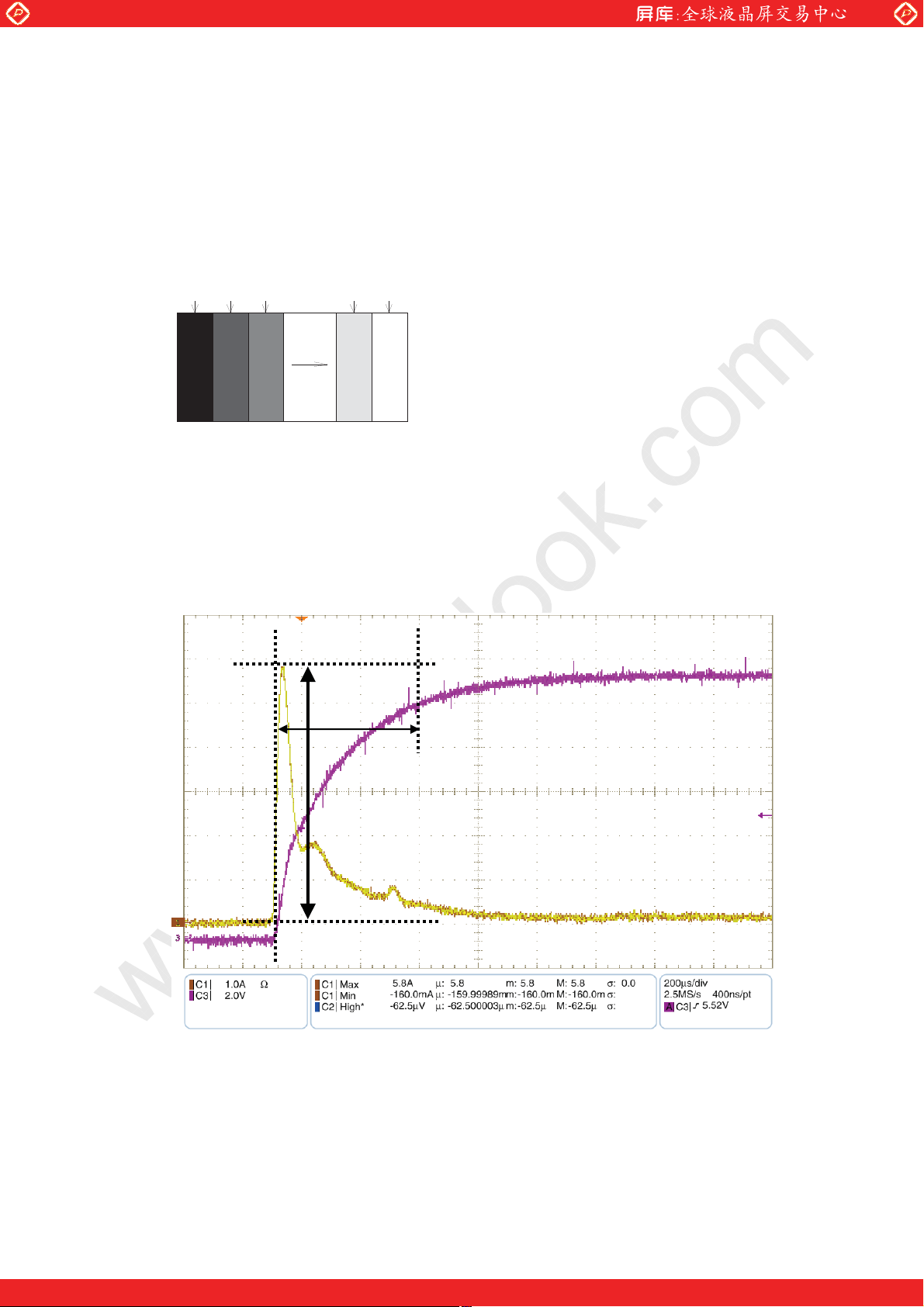
[Note 7] Vcc12V inrush current waveform (This figure is I
)$
)5
www.panelook.com
4)$
)5
CK㧩74.25MHz
Th㧩7.41s
RUSH
LD-K22553䙱10
Vcc㧩+12.0V
: t1=500Ǵs)
0.1Vcc
t
I
RUSH
1
Vcc= 12V
0.9Vcc
200Ǵs/div
One step solution for LCD / PDP / OLED panel application: Datasheet, inventory and accessory!
www.panelook.com
Page 13
Global LCD Panel Exchange Center
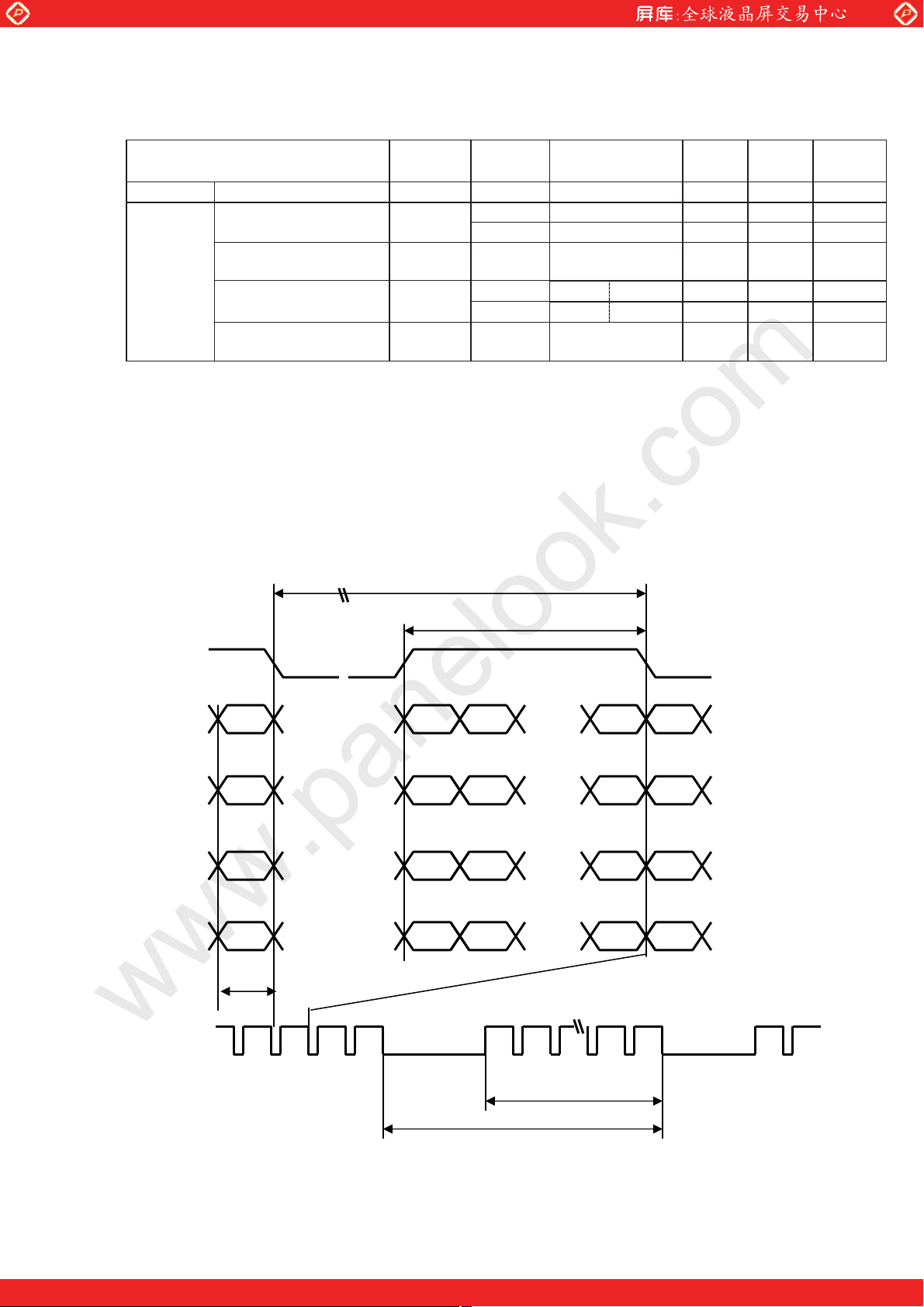
4.5 Timing characteristics of input signals for C-PWB
Timing diagrams of input signal are shown in Fig.2.
Parameter Symbol Min. Typ. Max. Unit Remark
www.panelook.com
LD-K22553䙱11
Clock Frequency 1/Tc 69
Horizontal period TH
Data enable
signal
Horizontal period
(High)
Vertical period TV
Vertical period
(High)
THd
TVd 1080 1080 1080 line
[Note]-When vertical period is very long, flicker and etc. may occur.
-Please turn off the module after it shows the black screen.
-Please make sure that length of vertical period should become of an integral multiple of horizontal
length of period. Otherwise, the screen may not display properly.
-As for your final setting of driving timing, we will conduct operation check test at our side, please
inform your final setting.
TH
DE
Aport DATA
1
5
(R,G,B)
Bport DATA
2
6
(R,G,B)
Cport DATA
1919 1919
3
7
(R,G,B)
Dport DATA
4
8 1920 1920
(R,G,B)
Tc
DE
TV
Fig.2.Timing characteristics of input signal
74.25
542 550
7.3 7.41
480 480
1096
88.2
THd
1 2 1080
1350
100
TVd
1125
120
1917 1917
1918 1918
1079
76
MHz
600 clock
8.1 μs
480 clock
1400
123.10
line
Hz
One step solution for LCD / PDP / OLED panel application: Datasheet, inventory and accessory!
www.panelook.com
Page 14

Global LCD Panel Exchange Center
4.6 Input data signal and display position on the screen
R1G1B1R2G2B2
㧝㨮㧝 㧝㧞
R3G3B3R4G4B4
㧝㨮㧟 㧝㧠
www.panelook.com
LD-K22553䙱12
㧝㧝㧝㧞㧝㧟
㧞㧝㧞㧞
㧟㧝
㨯
㧝㧠
RGB
Display position of Dat (V,H)
㨯
㨯
One step solution for LCD / PDP / OLED panel application: Datasheet, inventory and accessory!
www.panelook.com
Page 15

Global LCD Panel Exchange Center
4.7 LVDS signal characteristics
CLK-
Vo c
CLK+
Vo c
RINx-
Vo c
RINx+
Vo c
CLK-
CLK+
RINx-
Vdiff=0 Vdiff=0
RINx+
tpd0
tpd1
tpd2
tpd3
tpd4
tpd5
tpd6
The item Symbol min. typ. max. unit
Differential voltage Vod 200 400 600
Common mode voltage Voc Vod/2 1200
LVDS clock period t
Delay time, CLK rising
edge to serial bit position 0
Delay time, CLK rising
edge to serial bit position 1
Delay time, CLK rising
edge to serial bit position 2
Data
position
Delay time, CLK rising
edge to serial bit position 3
Delay time, CLK rising
edge to serial bit position 4
Delay time, CLK rising
edge to serial bit position 5
Delay time, CLK rising
edge to serial bit position 6
www.panelook.com
t
CLK
12.35 13.50 13.69
CLK
tpd0
tpd1
tpd2
tpd3
tpd4
tpd5
tpd6
1*t
2* t
3* t
4* t
5* t
6* t
LD-K22553䙱13
Vod
Vod
mV
2400㧙Vo d / 2
-0.25 0 0.25
/7-0.25 1* t
CLK
/7-0.25 2* t
CLK
/7-0.25 3* t
CLK
/7-0.25 4* t
CLK
/7-0.25 5* t
CLK
7-0.25 6* t
CLK
/7 1* t
CLK
/7 2* t
CLK
/7 3* t
CLK
/7 4* t
CLK
/7 5* t
CLK
/7 6* t
CLK
/7+0.25
CLK
/7+0.25
CLK
/7+0.25
CLK
/7+0.25
CLK
/7+0.25
CLK
/7+0.25
CLK
ns
One step solution for LCD / PDP / OLED panel application: Datasheet, inventory and accessory!
www.panelook.com
Page 16
Global LCD Panel Exchange Center
5 Input Signal, Basic Display Color and Gray scale of Each Color
Colors &
Gray scale
Black – 0 0 0 0 0 0 0 0 0 0 0 0 0 0 0 0 0 0 0 0 0 0 0 0 0 0 0 0 0 0
Blue – 0 0 0 0 0 0 0 0 0 0 0 0 0 0 0 0 0 0 0 0 1 1 1 1 1 1 1 1 1 1
Green – 0 0 0 0 0 0 0 0 0 0 1 1 1 1 1 1 1 1 1 1 0 0 0 0 0 0 0 0 0 0
Cyan – 0 0 0 0 0 0 0 0 0 0 1 1 1 1 1 1 1 1 1 1 1 1 1 1 1 1 1 1 1 1
Red – 1 1 1 1 1 1 1 1 1 1 0 0 0 0 0 0 0 0 0 0 0 0 0 0 0 0 0 0 0 0
Basic Color
Magenta – 1 1 1 1 1 1 1 1 1 1 0 0 0 0 0 0 0 0 0 0 1 1 1 1 1 1 1 1 1 1
Yellow – 1 1 1 1 1 1 1 1 1 1 1 1 1 1 1 1 1 1 1 1 0 0 0 0 0 0 0 0 0 0
White – 1 1 1 1 1 1 1 1 1 1 1 1 1 1 1 1 1 1 1 1 1 1 1 1 1 1 1 1 1 1
Black GS0 0 0 0 0 0 0 0 0 0 0 0 0 0 0 0 0 0 0 0 0 0 0 0 0 0 0 0 0 0 0
× GS1 1 0 0 0 0 0 0 0 0 0 0 0 0 0 0 0 0 0 0 0 0 0 0 0 0 0 0 0 0 0
R0 R1 R2 R3 R4 R5 R6 R7 R8 R9 G0 G1 G2 G3 G4 G5 G6 G7 G8 G9 B0 B1 B2 B3 B4 B5 B6 B7 B8 B9
Gray
Scale
www.panelook.com
LD-K22553䙱14
Data signal
Darker GS2 0 1 0 0 0 0 0 0 0 0 0 0 0 0 0 0 0 0 0 0 0 0 0 0 0 0 0 0 0 0
×
Ø
Brighter GS1021 1 0 1 1 1 1 1 1 1 1 0 0 0 0 0 0 0 0 0 0 0 0 0 0 0 0 0 0 0 0
p
p
p
p
p
p
p
p
Gray Scale of Red
Ø GS1022 0 1 1 1 1 1 1 1 1 1 0 0 0 0 0 0 0 0 0 0 0 0 0 0 0 0 0 0 0 0
Red GS1023 1 1 1 1 1 1 1 1 1 1 0 0 0 0 0 0 0 0 0 0 0 0 0 0 0 0 0 0 0 0
Black GS0 0 0 0 0 0 0 0 0 0 0 0 0 0 0 0 0 0 0 0 0 0 0 0 0 0 0 0 0 0 0
× GS1 0 0 0 0 0 0 0 0 0 0 1 0 0 0 0 0 0 0 0 0 0 0 0 0 0 0 0 0 0 0
Darker GS2 0 0 0 0 0 0 0 0 0 0 0 1 0 0 0 0 0 0 0 0 0 0 0 0 0 0 0 0 0 0
×
Ø
Brighter GS1021 0 0 0 0 0 0 0 0 0 0 1 0 1 1 1 1 1 1 1 1 0 0 0 0 0 0 0 0 0 0
Gray Scale of Green
Ø GS1022 0 0 0 0 0 0 0 0 0 0 0 1 1 1 1 1 1 1 1 1 0 0 0 0 0 0 0 0 0 0
Green GS1023 0 0 0 0 0 0 0 0 0 0 1 1 1 1 1 1 1 1 1 1 0 0 0 0 0 0 0 0 0 0
Black GS0 0 0 0 0 0 0 0 0 0 0 0 0 0 0 0 0 0 0 0 0 0 0 0 0 0 0 0 0 0 0
× GS1 0 0 0 0 0 0 0 0 0 0 0 0 0 0 0 0 0 0 0 0 1 0 0 0 0 0 0 0 0 0
Darker GS2 0 0 0 0 0 0 0 0 0 0 0 0 0 0 0 0 0 0 0 0 0 1 0 0 0 0 0 0 0 0
Ø
Ø
Brighter GS1021 0 0 0 0 0 0 0 0 0 0 0 0 0 0 0 0 0 0 0 0 1 0 1 1 1 1 1 1 1 1
Gray Scale of Blue
Ø GS1022 0 0 0 0 0 0 0 0 0 0 0 0 0 0 0 0 0 0 0 0 0 1 1 1 1 1 1 1 1 1
p
p
p
p
p
p
p
p
p
p
p
p
p
p
p
p
Blue GS1023 0 0 0 0 0 0 0 0 0 0 0 0 0 0 0 0 0 0 0 0 1 1 1 1 1 1 1 1 1 1
0: Low level voltage, 1: High level voltage.
Each basic color can be displayed in 1024 gray scales from 10 bits data signals. According to the combination of
total 30 bits data signals, one billion-color display can be achieved on the screen.
One step solution for LCD / PDP / OLED panel application: Datasheet, inventory and accessory!
www.panelook.com
Page 17

Global LCD Panel Exchange Center
Optical characteristics
6 Optical Specifications
6.1 O
Parameter Symbol Condition Min. Typ. Max. Unit Remark
Viewing angle
range
Contrast ratio CRn - 5000 - - [Note2,4]
Horizontal
Vertical
www.panelook.com
(Reference value)
T
T
T
T
21
22
11
12
CR>
10
Ta=25qC, Vcc=12.0V, Timing:120Hz(typ. value)
70 88 - Deg.
70 88 -
Deg.
LD-K22553䙱15
[Note1,4]
Response time
White
Red
Luminance
Green
Blue
Transmittance T
Luminance
uniformity
-Optical characteristics are based on SHARP standard module LK400D3LA14
-The measurement shall be executed 60 minutes after lighting at rating.
[Note]The optical characteristics are measured using the following equipment.
Detector㧔EZ-CONTRAST/ Photodiode㧕
Center of the screen (T㧩0q)
TFT-LCD Module
Fig.3-1 Measurement of viewing angle range and
Response time.
White
Viewing angle range: EZ-CONTRAST
Response time: Photodiode
W
DRV
Gw
x
y
x
y
x
y
x
y
T
=0 deg.
T
=0 deg.
- - 1.25 [Note 6]
4 ms [Note3,4,5]
Typ.-0.03 0.278 Typ.+0.03
Typ.-0.03 0.285 Typ.+0.03
Typ.-0.03 0.644 Typ.+0.03
Typ.-0.03 0.344 Typ.+0.03
Typ.-0.03 0.284 Typ.+0.03
Typ.-0.03 0.607 Typ.+0.03
Typ.-0.03 0.147 Typ.+0.03
Typ.-0.03 0.069 Typ.+0.03
- 6.16 - %
400mm
Center of the screen (T㧩0q)
TFT-LCD Module
Fig.3-2 Measurement of Contrast, Luminance,
Chromaticity.
-
-
-
-
-
-
-
-
Detector㧔SR-3A-UL1Equivalent goods㧕
Field=1q
[Note4]
One step solution for LCD / PDP / OLED panel application: Datasheet, inventory and accessory!
www.panelook.com
Page 18

Global LCD Panel Exchange Center
[Note 1]Definitions of viewing angle range :
T
22
T
12
[Note 2]Definition of contrast ratio :
The contrast ratio is defined as the following.
Luminance (brightness) with all pixels white
Contrast Ratio
Luminance (brightness) with all pixels black
[Note 3]Definition of response time
The response time (W
and Wr) is defined as the following figure and shall be measured by switching the input
d
signal for “any level of gray (0%, 25%, 50%, 75% and 100%)” and “any level of gray (0%, 25%, 50%, 75%
and 100%)”.
www.panelook.com
Normal line
T
11
6 o’clock direction
㧩
T
LD-K22553䙱16
21
0%
0%
25㧑
50㧑
75㧑
100%
td: 25%-0㧑
td: 50%-0㧑 td: 50%-25㧑
td: 75%-0㧑 td: 75%-25㧑 td: 75%-50㧑
td: 100%-0㧑 td: 100%-25㧑 td: 100%-50㧑 td:100%-75㧑
25㧑 50㧑 75㧑
tr:0%-25㧑
tr:0%-50% tr:0%-75% tr:0%-100%
tr: 25%-50㧑 tr25%-75㧑 tr: 25%-100㧑
tr: 50%-75㧑 tr: 50%-100㧑
100%
tr: 75%-100㧑
t*:x-y...response time from level of gray(x) to level of gray(y)
= 6(tr:x-y)/10 , Wd = 6(td:x-y)/10
W
r
Bright
100%
90%
Dark
Bright
Photodetector
10%
Output
0%
Wd Wr
time
[Note 4]This shall be measured at center of the screen.
[Note 5] This value is valid when O/S driving is used at typical input time value.
One step solution for LCD / PDP / OLED panel application: Datasheet, inventory and accessory!
www.panelook.com
Page 19

Global LCD Panel Exchange Center
[Note 6]Definition of white uniformity ;
White uniformity is defined as the following with five measurements. (AaE)
Maximum luminance of five points (brightness)
㨃㧩
G
Minimum luminance of five points (brightness)
www.panelook.com
480
960 1440
A㩷
C㩷
B㩷
LD-K22553䙱17
pixel
D㩷
E㩷
270
540
810
pixel
㩷
One step solution for LCD / PDP / OLED panel application: Datasheet, inventory and accessory!
www.panelook.com
Page 20
Global LCD Panel Exchange Center
LK400D3JA14*
㧔
㧠㧿
㧕
LK400D3HA㧖㧖
㧔
㧠㧿
㧕
Y
V
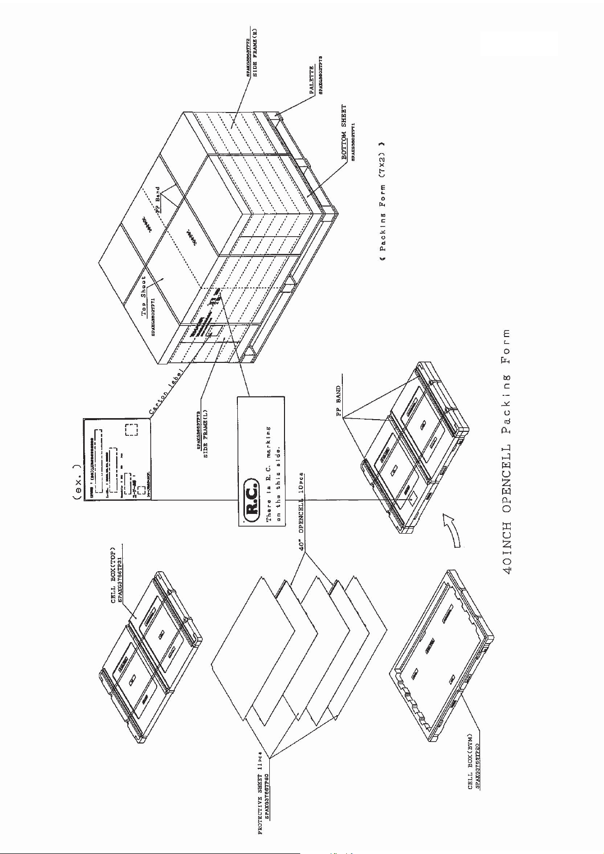
7 Shipping and Packing
7.1 Packing form
a) Piling number of cell boxes : 14cell box/1 palette
b) Packing quantity in one cell box :10pcs
c) Carton size :1360(W)112(D)1063(H)
d) Total mass of one carton filled with full cell :428.5kg Max
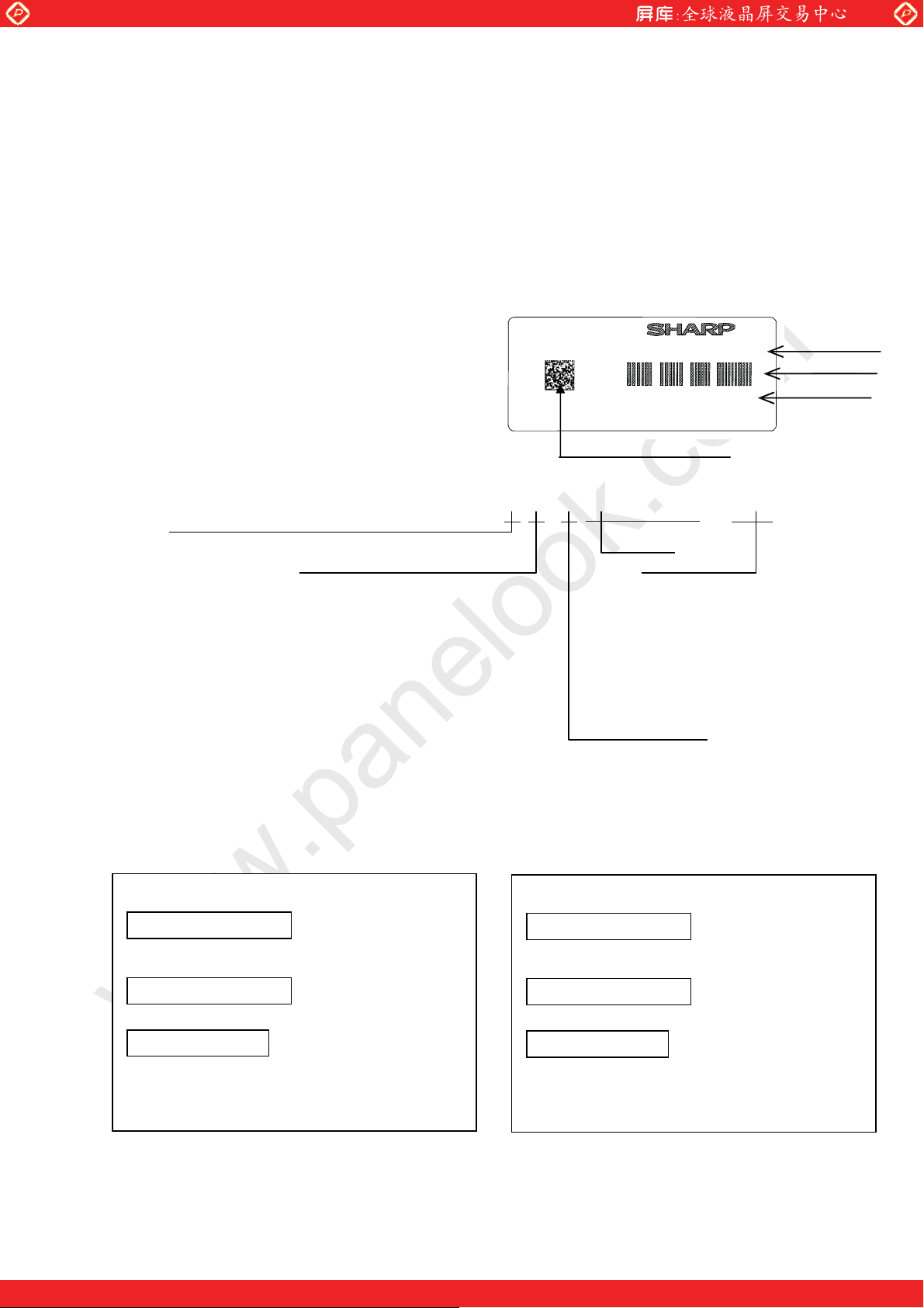
7.2 Label
a) Cell Label
This label is stuck on the protection film of front polarizer.
ޣLK400D3HA㧖㧖ޤ JAPAN PRODUCTION
[LK400D3HA㧖㧖]
␠ౝຠ⇟㧦
㧽㨡㨍㨚㨠㨕㨠㨥㧦
࡙ࠩຠ⇟
ࠪࡖࡊ‛ᵹ↪ࡌ࡞ߢߔޕ
A production year(the last figures of the Christian Era)
b) Packing Label
This Label is stuck on the packing case(cell box) and carton.
b-1)Cell box b-2)Carton
Bar code Ԙ
㧸㨛㨠㧺㧻㧚
Bar codeԙ
Bar code Ԛ
ԘManagement No
ԙLot No.(Date)
ԚQuantity
㧔㧝㨀㧕㧞㧜㧖㧖㧖㧖㧖
㧔㧽㧕
www.panelook.com
A production month (1-9, X,Y, Z)
㨜㨏㨟
㪈
䌌䌋䋴 䋰 䋰䌄䋳
HA㧖㧖
䋪
2D Barcode
How to express Lot No.
٤٤ ٤ ٤ ٤ ٤ ٤ 㧙 㧙
٤
Serial No.
Management No.
K: Kameyama Plant.
L: Kameyama Tec. Kameyama Fab.
N: NSEC
F: DID
: TPV
: TOT
␠ౝຠ⇟㧦
Bar code Ԙ
㧸㨛㨠㧺㧻㧚
Bar codeԙ
㧽㨡㨍㨚㨠㨕㨠㨥㧦
Bar code Ԛ
࡙ࠩຠ⇟
ࠪࡖࡊ‛ᵹ↪ࡌ࡞ߢߔޕ
㧔㧝㨀㧕㧞㧜㧖㧖㧖㧖㧖
㧔㧽㧕
LD-K22553䙱18
%GNN 0Q
$CTEQFG
.QV 0Q
㨜㨏㨟
One step solution for LCD / PDP / OLED panel application: Datasheet, inventory and accessory!
www.panelook.com
Page 21
Global LCD Panel Exchange Center
8 Carton storage condition.
Temperature 0°C to 40°C
Humidity 95%RH or less
Reference condition : 20°C to 35°C, 85%RH or less (summer)
: 5°C to 15°C, 85%RH or less (winter)
· the total storage time (40°C, 95%RH) : 240H or less
Sunlight Be sure to shelter a product from the direct sunlight.
Atmosphere Harmful gas, such as acid and alkali which bites electronic components and/or
wires must not be detected.
Notes Be sure to put cartons on palette or base, don’t put it on floor, and store them with
removing from wall
Please take care of ventilation in storehouse and around cartons, and control
changing temperature is within limits of natural environment
Storage life 1 year
9 Reliability
Reliability test item
No. Test item Condition
1
2
3
4
5
Above tests are executed under the CCFL module conditions.
High temperature storage test
Low temperature storage test
High temperature and high humidity
operation test
High temperature operation test
Low temperature operation test
10Precautions
a) Since the polarizer is easily damaged, pay attention not to scratch it.
b) Since long contact with water may cause discoloration or spots, wipe off water drop immediately.
c) When the polarizer is soiled, wipe it with absorbent cotton or other soft cloth.
d) Since the panel is made of glass, it may break or crack if dropped or bumped on hard surface. Handle with
care.
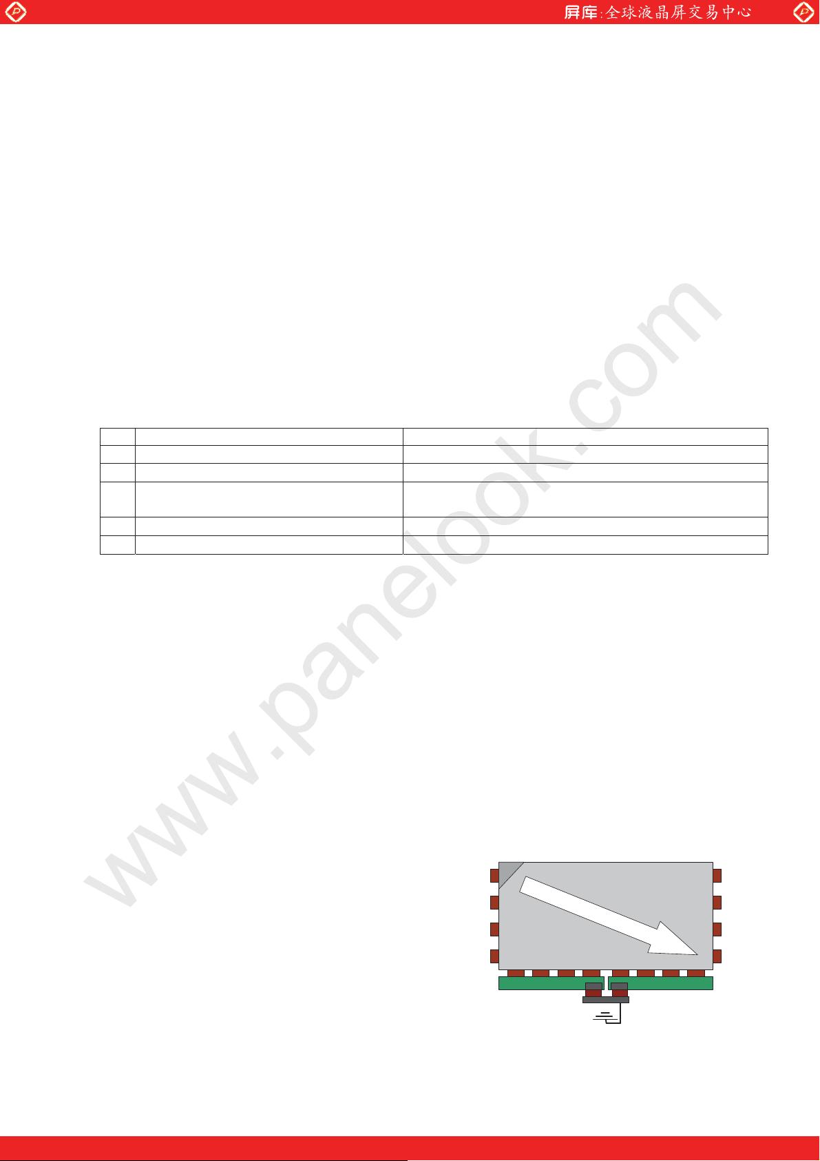
e) Precautions of peeling off the protection film.
- Be sure to peel off slowly (recommended more than 7sec) and constant speed.
- Peeling direction shows Fig.
- Be sure to ground person with adequate methods such as the anti-static wrist band.
- Be sure to ground S-PWB while peeling of the protection film.
- Ionized air should be blown over during peeling action.
- The protection film must not touch drivers and S-PWBs.
- If adhesive may remain on the polarizer after the
protection film peeling off,
please remove with isopropyl-alcohol.
www.panelook.com
LD-K22553䙱19
Ta=60qC240h
Ta=-25qC 240h
Ta=40qC ; 95%RH 240h
(No condensation)
Ta=50qC 240h
Ta=0qC 240h
One step solution for LCD / PDP / OLED panel application: Datasheet, inventory and accessory!
www.panelook.com
Page 22

Global LCD Panel Exchange Center
f) Since the Open Cell consists of TFT and electronic circuits with CMOS-ICs, which are very weak to
electrostatic discharges, persons who are handling the Open Cell should be grounded through adequate
methods such as the anti-static wrist band. Connector pins should not be touched directly with bare hands.
- Reference : Process control standard of sharp
Item Management standard value and performance standard
1 Anti-static mat (floor) 1 to 50 [M ohm]
2 Anti-static mat (shelf, desk) 1 to 100 [M ohm]
3 Ionizer Attenuate from +1000V to +100V within 2 sec
4 Anti-static wrist band 0.8 to 10 [M ohm]
5 Anti-static wrist band entry and
ground resistance
6 Temperature 22 to 26 [oC]
7 Humidity 60 to 70 [%RH]
g) The Open Cell has some PWBs, take care to keep them from any stress or pressure when handling or
installing the Open Cell, otherwise some of electronic parts on the PWBs may be damaged.
h) Be sure to turn off the power supply when inserting or disconnecting the cable.
i) Be sure to design the module and cabinet so that the Open Cell can be installed without any extra stress
such as warp or twist.
j) When handling the Open Cell and assembling them into module and cabinets, please be noted that
long-term storage in the environment of oxidization or deoxidization gas and the use of such materials as
reagent, solvent, adhesive, resin, etc. which generate these gasses, may cause corrosion and discoloration
of the Open Cell.
k) Applying too much force and stress to PWB and driver may cause a malfunction electrically and
mechanically.
l) The Open Cell has high frequency circuits. Sufficient suppression to EMI should be done by system
manufacturers.
m) Please be careful since image retention may occur when a fixed pattern is displayed for a long time.
n) The chemical compound, which causes the destruction of ozone layer, is not used.
o) This Open Cell is corresponded to RoHS. ‘‘R.C.’’ label on the side of palette shows it.
p) When any question or issue occurs, it shall be solved by mutual discussion.
www.panelook.com
LD-K22553䙱20
Below 1000 [ohm]
One step solution for LCD / PDP / OLED panel application: Datasheet, inventory and accessory!
www.panelook.com
Page 23

Global LCD Panel Exchange Center
www.panelook.com
One step solution for LCD / PDP / OLED panel application: Datasheet, inventory and accessory!
www.panelook.com
Page 24
Global LCD Panel Exchange Center
www.panelook.com
LD-K22553-22
One step solution for LCD / PDP / OLED panel application: Datasheet, inventory and accessory!
www.panelook.com
 Loading...