

Page 1
Page 2
RECORDS OF REVISION
MODEL No. : LK400D3HA3K
SPEC No. : LD-K22223A
DATE
NO.
2010.02.23
LD-K22223
REVISED
2010.04.12 LD-K22223A A
No.
PAGE SUMMARY NOTE
- - - 1st Issue
All Reformat of all pages
10
[Add]Scan Direction
[Change]Optical calacteristics
2nd Issue
13
Chromaticity ,Luminance uniformity
[Change]Optical calacteristics[Note6]
15
Definition of white uniformity(5point -> 9point)
[Add]Optical characteristics[Note7]
15
[Add]Reliability test item
16
Page 3
LD-K22223A-1
1 Application
This specification applies to the color 40.0” TFT-LCD Open Cell LK400D3HA3K
* This specification is proprietary products of SHARP CORPORATION (“SHARP”) and include materials protected
under copyright of SHARP. Do not reproduce or cause any third party to reproduce them in any form or by any
means, electronic or mechanical, for any purpose, in whole or in part, without the express written permission of
SHARP.
* In case of using the device for applications such as control and safety equipment for transportation (aircraft, trains,
automobiles, etc.), rescue and security equipment and various safety related equipment which require higher
reliability and safety, take into consideration that appropriate measures such as fail-safe functions and redundant
system design should be taken.
* Do not use the device for equipment that requires an extreme level of reliability, such as aerospace applications,
telecommunication equipment (trunk lines), nuclear power control equipment and medical or other equipment for
life support.
* SHARP assumes no responsibility for any damage resulting from the use of the device that does not comply with
the instructions and the precautions specified in these technical literature.
* Contact and consult with a SHARP sales representative for any questions about this device.
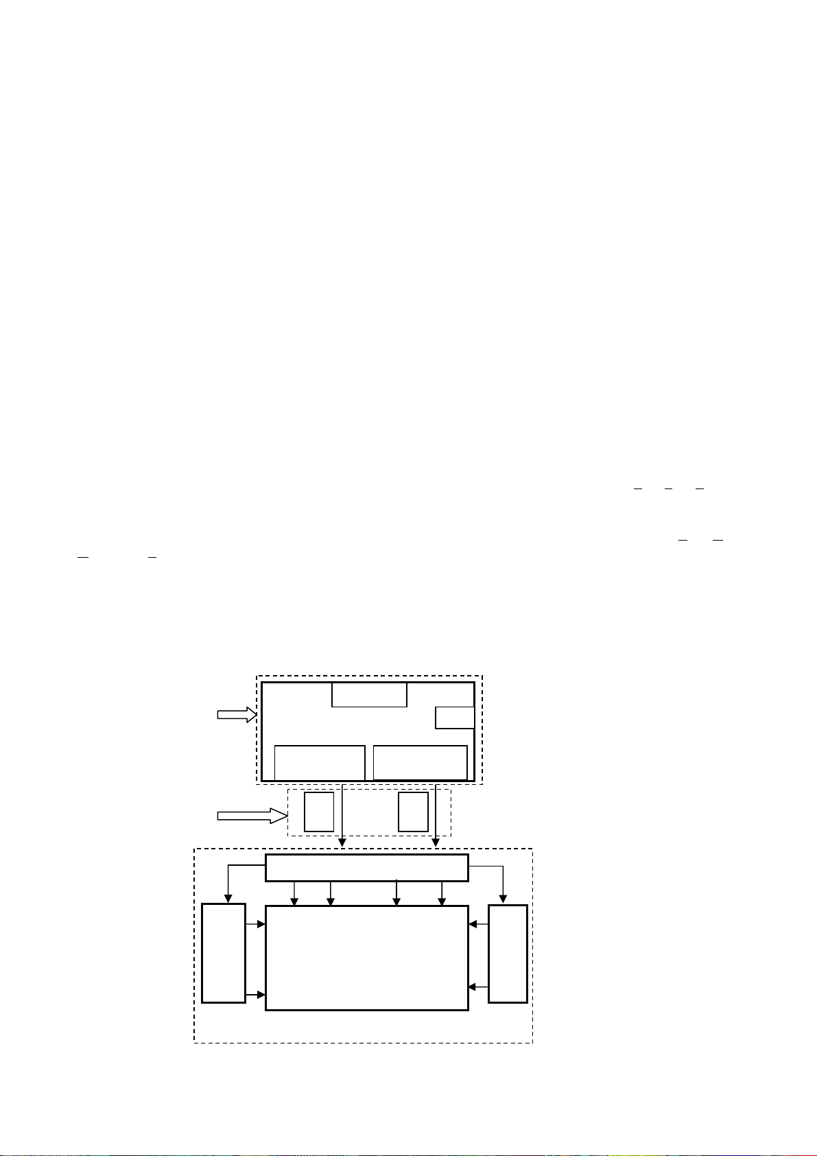
2 Overview
This Open Cell is a color active matrix LCD Open-Cell incorporating amorphous silicon TFT (Thin Film Transistor).
It is composed of a color TFT-LCD panel, driver ICs and Source PWB. The following content can be achieved in
using LK0DZ1C0115 (C-PWB) and LK0DZ1C0114 (FPC) that SHARP specifies. Graphics and texts can be
displayed on a 1920×RGB×1080 dots panel with one billion colors by using 10bit+ LVDS (L
ifferential Signaling) to interface, +12V of DC supply voltages.
D
And in order to improve the response time of LCD, This module applies the Over Shoot driving (O/S driving)
technology for the control circuit .In the O/S driving technology, signals are being applied to the Liquid Crystal
according to a pre-fixed process as an image signal of the present frame when a difference is found between image
signal of the previous frame and that of the current frame after comparing them.
With combination of these technologies, motion blur can be reduced and clearer display performance can be
realized.
ow Voltage
CN1
Power Supply
SOURCE DRIVER
LCD PANEL
CN3
Circuit
FPC
GATE DRIVER
LK0DZ1C0115
LK0DZ1C0114
CONTROL PWB
Control Signals
FPC
GATE DRIVER
1920×3(RGB)×1080
LK400D3HA3K (Open Cell)
Page 4
3 Mechanical Specifications
Parameter Specifications Unit
Display size
Active area 885.6H) x 498.15 (V) mm
Pixel Format
Pixel pitch 461.25(H) x 461.25 (V) um
Pixel configuration R, G, B vertical stripe
Display mode Normally black
Open Cell Outline Dimensions
[Note1]
Mass
Surface treatment[[Note2]
[Note1]Outline Dimensions are shown fig.1
[Note2]With the protection film removed.
101.609 (Diagonal)
40.0 (Diagonal)
1920(H) x 1080(V)
(1pixel = R + G + B dot)
921.18(H) x 555.7(V) x 1.82(D)
1.88 ±0.3
- Front polarizer : Glare
Hard coating: 2H and more
- Rear polarizer :
Hard coating less (B)
4 Open Cell Driving Specifications
4.1
Driving interface of Control PWB SHARP specifies[LK0DZ1C0115]
CN1 (Interface signals and +12V DC power supply)
Using connector : PF050-C82B-C35 (UJU Electronics Co, Ltd.)
Mating LVDS transmitter : THC63LVD1023 or equivalent device
Pin No. Symbol Function Remark
1 VCC
2 VCC +12V Power Supply
3 VCC +12V Power Supply
4 VCC +12V Power Supply
5 VCC +12V Power Supply
6 Reserved It is required to set non-connection(OPEN)
7 GND
8 GND
9 GND
10
11
12
13
14
15
16 GND
17
18
19
20
21
22
23
24 GND
25
26
27
28
29
30
AIN0-
AIN0+
AIN1-
AIN1+
AIN2-
AIN2+
ACK-
ACK+
GND
AIN3-
AIN3+
AIN4-
AIN4+
CIN0-
CIN0+
CIN1-
CIN1+
CIN2-
CIN2+
+12V Power Supply
Aport (-)LVDS CH0 differential data input
Aport (+)LVDS CH0 differential data input
Aport (-)LVDS CH1 differential data input
Aport (+)LVDS CH1 differential data input
Aport (-)LVDS CH2 differential data input
Aport (+)LVDS CH2 differential data input
Aport LVDS Clock signal(-)
Aport LVDS Clock signal(+)
Aport (-)LVDS CH3 differential data input
Aport (+)LVDS CH3 differential data input
Aport (-)LVDS CH4 differential data input
Aport (+)LVDS CH4 differential data input
Cport (-)LVDS CH0 differential data input
Cport (+)LVDS CH0 differential data input
Cport (-)LVDS CH1 differential data input
Cport (+)LVDS CH1 differential data input
Cport (-)LVDS CH2 differential data input
Cport (+)LVDS CH2 differential data input
LD-K22223A-2
cm
inch
pixel
mm
kg
Page 5
LD-K22223A-3
31
32
33
34
35
36
37
38
39 GND
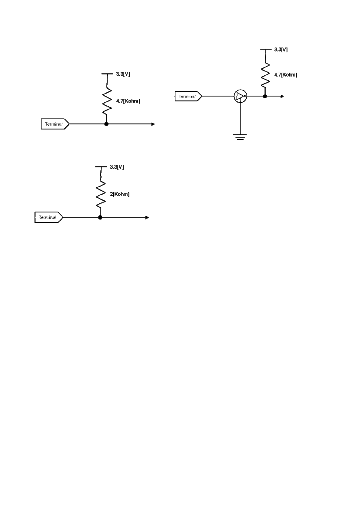
40 I2C_SCL I2C CLK Pull up 3.3V[Note1]
41 Reserved It is required to set non-connection(OPEN)
42 Reserved
43 WP
44 I2C_SDA I2C DATA Pull up 3.3V[Note1]
45 SELLVDS
46 Reserved
47 Reserved It is required to set non-connection(OPEN)
48 Reserved
49 Reserved
50 Reserved
51 Reserved
52 GND
53 DIN4+
54 DIN455 DIN3+
56 DIN357 GND
58 DCK+
59 DCK60 GND
61 DIN2+
62 DIN263 DIN1+
64 DIN165 DIN0+
66 DIN067 GND
68 BIN4+
69 BIN470 BIN3+
71 BIN372 GND
73 BCLK+
74 BCLK75 GND
76 BIN2+
77 BIN278 BIN1+
79 BIN180 BIN0+
81 BIN082 GND
GND
CCK-
CCK+
GND
CIN3-
CIN3+
CIN4-
CIN4+
Cport LVDS Clock signal(-)
Cport LVDS Clock signal(+)
Cport (-)LVDS CH3 differential data input
Cport (+)LVDS CH3 differential data input
Cport (-)LVDS CH4 differential data input
Cport (+)LVDS CH4 differential data input
It is required to set non-connection(OPEN)
I2C bus enable(L/Open:enable, H:disable)
Select LVDS data order [Note4]
It is required to set non-connection(OPEN)
It is required to set non-connection(OPEN)
It is required to set non-connection(OPEN)
It is required to set non-connection(OPEN)
It is required to set non-connection(OPEN)
Dport (+)LVDS CH4 differential data input
Dport (-)LVDS CH4 differential data input
Dport (+)LVDS CH3 differential data input
Dport (-)LVDS CH3 differential data input
Dport LVDS Clock signal(+)
Dport LVDS Clock signal(-)
Dport (+)LVDS CH2 differential data input
Dport (-)LVDS CH2 differential data input
Dport (+)LVDS CH1 differential data input
Dport (-)LVDS CH1 differential data input
Dport (+)LVDS CH0 differential data input
Dport (-)LVDS CH0 differential data input
Bport (+)LVDS CH4 differential data input
Bport (-)LVDS CH4 differential data input
Bport (+)LVDS CH3 differential data input
Bport (-)LVDS CH3 differential data input
Bport LVDS Clock signal(+)
Bport LVDS Clock signal(-)
Bport (+)LVDS CH2 differential data input
Bport (-)LVDS CH2 differential data input
Bport (+)LVDS CH1 differential data input
Bport (-)LVDS CH1 differential data input
Bport (+)LVDS CH0 differential data input
Bport (-)LVDS CH0 differential data input
[Note2]
Pull up 3.3V[Note3]
Page 6
LD-K22223A-4
[note] GND of a liquid crystal panel drive part should be connected with a module chassis..
[Note 1] The equivalent circuit figure of the terminal [Note2] The equivalent circuit figure of the terminal
[Note3] The equivalent circuit figure of the terminal
Page 7
[Note 4] LVDS Data order
Data L(GND)
TA0
TA1
TA2
TA3
TA4
TA5
TA6
TB0
TB1
TB2
TB3
TB4
TB5
TB6
TC0
TC1
TC2
TC3
TC4 NA NA
TC5 NA NA
TC6 DE(*) DE(*)
TD0
TD1
TD2
TD3
TD4
TD5
TD6
TE0
TE1
TE2
TE3
TE4
TE5
TE6
NA: Not Available
(*)Since the display position is prescribed by the rise of DE(Display Enable)signal, please do not fix DE
signal during operation at ”High”.
SELLVDS
[VESA]
R0(LSB)
R1
R2
R3
R4
R5
G0(LSB)
G1
G2
G3
G4
G5
B0(LSB)
B1
B2
B3
B4
B5
R6
R7
G6
G7
B6
B7
N/A
R8
R9(MSB)
G8
G9(MSB)
B8
B9(MSB)
N/A
LD-K22223A-5
H(3.3V) or Open
[JEIDA]
R4
R5
R6
R7
R8
R9(MSB)
G4
G5
G6
G7
G8
G9(MSB)
B4
B5
B6
B7
B8
B9(MSB)
R2
R3
G2
G3
B2
B3
N/A
R0(LSB)
R1
G0(LSB)
G1
B0(LSB)
B1
N/A
Page 8
SELLVDS= Low (GND)
NA
NA
NA
N
NA
NA
NA
NA
NA
N
NA
NA
ACK+, BCK+
CCK+, DCK+
ACK-, BCKCCK-, DCK-
AIN0+, BIN0+
CIN0+, DIN0+
AIN0-, BIN0CIN0-, DIN0-
AIN1+, BIN1+
CIN1+, DIN1+
AIN1-, BIN1CIN1-, DIN1-
AIN2+, BIN2+
CIN2+, DIN2+
AIN2-, BIN2CIN2-, DIN2-
AIN3+, BIN3+
CIN3+, DIN3+
AIN3-, BIN3CIN3-, DIN3-
1cycle
R1 R0 G0 R5 R4 R3 R2 R1 R0 G0
G2 G1 B1 B0 G5 G4 G3 G2 G1 B1
B3 B6 DE
R7 R6
B7 B6 G7 G6 R7 R6
B5 B4 B3 B2 DE
LD-K22223A-6
A
AIN4+, BIN4+
CIN4+, DIN4+
AIN4-, BIN4CIN4-, DIN4-
R9 R8
SELLVDS= High (3.3V) or OPEN
ACK+, BCK+
CCK+, DCK+
ACK-, BCKCCK-, DCK-
AIN0+, BIN0+
CIN0+, DIN0+
AIN0-, BIN0CIN0-, DIN0-
AIN1+, BIN1+
CIN1+, DIN1+
AIN1-, BIN1CIN1-, DIN1-
AIN2+, BIN2+
CIN2+, DIN2+
AIN2-, BIN2CIN2-, DIN2-
R5 R4 G4 R9 R8 R7 R6 R5 R4 G4
G6 G5 B5 B4 G9 G8 G7 G6 G5 B5
B7 B6 DE
B9 B8 G9 G8 R9 R8
1cycle
B9 B8 B7 B6 DE
AIN3+, BIN3+
CIN3+, DIN3+
AIN3-, BIN3CIN3-, DIN3-
AIN4+, BIN4+
CIN4+, DIN4+
AIN4-, BIN4CIN4-, DIN4-
R3 R2
R1 R0
B3 B2 G3 G2 R3 R2
B1 B0 G1 G0 R1 R0
A
DE: Display Enable, NA: Not Available (Fixed Low)
Page 9

LD-K22223A-7
4.2
Vcom Adjusting interface of Control PWB SHARP specifies[LK0DZ1C0115]
CN3(Interface Vcom Adjusting)
[note1]
Interface : 1.5mm Pitch Via Hole(0.7mm phi)
Mating connector : (housing)3P-SZN, (contact)SZN-002T-P0.7K (JST Co.,Ltd.)
Pin No. Symbol Function Remark
1 SDA
I2C DATA
Pull up 3.3V[Note2]
2 SCL I2C CLK Pull up 3.3V[Note2]
3 GND
[Note1]Interface [Note2] The equivalent circuit figure of the terminal
3.3[V]
3.3[V]
PinNo Symbol
3 GND
2 SCL
1 SDA
10[Kohm]
10[Kohm]
Terminal
TerminalTerminal
4.3
Absolute Maximum Ratings
Parameter Symbol Condition Ratings Unit Remark
Input voltage
(for Control)
12V supply voltage
(for Control)
I
V
VCC
Ta=2 5 °C
Ta=2 5 °C
-0.3 ~ 3.6 V [Note 1]
0 ~ + 14 V
Storage temperature Tstg - -25 ~ +60
Operation temperature
(Ambient)
Topa - 0 ~ +50
[Note 1] SELLVDS
[Note 2] Humidity 95%RH Max.(Ta≦40°C)
Maximum wet-bulb temperature at 39 °C or less.(Ta>40°C)
No condensation.
4.4
Electrical Characteristics of input signals
Parameter Symbol Min. Typ. Max. Uniit Remark
Supply voltage Vcc 11.4 12 12.6 V [Note 1]
+12V supply
voltage
Current dissipation Icc - 0.8 2.9 A [Note 2]
I
Inrush current
RUSH
I
RUSH
Permissible input ripple voltage VRP - - 100 mVP-P Vcc = +12.0V
Input Low voltage VIL 0 - 0.8 V
Input High voltage VIH 2.0 - 3.3 V
Input leak current (Low) IIL1 - - 400 µA
Input leak current (High) IIH1 - - 400 µA
Terminal resistor RT - 100 - Ohm
Input Differential voltage |VID| 200 400 600 mV [Note 5]
Differential input
common mode voltage
VCM |VID|/2 1.2
[Note] VCM: Common mode voltage of LVDS driver.
°C
[Note 2]
°C
Ta=2 5 °C
1 - 4.5 - A
t1=500us
[Note 6]
2 - 2.5 - A t1>5ms
[Note 3]
I = 0V
V
[Note 4]
I = 3.3V
V
[Note 4]
Differential
input
2.4-
|VID|/2
V
[Note 5]
Page 10

LD-K22223A-8
0
[Note 1]
Input voltage sequences Dip conditions for supply voltage
0 < t1 < 20ms a) V2 ≦ Vcc < V1
20ms < t2 < 5s td < 10ms
20ms < t3 < 5s b) Vcc < V2
0 < t4 < 1s Dip conditions for supply voltage is
t5-1 > 1s based on input voltage sequence.
t5-2 > 1s
t6 -1> 0
t6 -2> 0
t7 > 1s
0.9VCC
.1Vcc
Vcc
t1
Data1
Data2
Back light:VON
t2
t3
t5-2
t5-1
OFF
ON
ON
t6-2
t6- 1
0.9Vcc
0.1Vc c
t4
t3
OFF
t7
0.1V cc
Vcc
V1=10.8V
V2=9.1V
td
※ Data1: ACK±, AIN0±, AIN1±, AIN2±, AIN3±, AIN4±,BCK±, BIN0±, BIN1±, BIN2±, BIN3±, BIN4±
CCK±, CIN0±, CIN1±, CIN2±, CIN3±, CIN4±, DCK±, DIN0±, DIN1±, DIN2±, DIN3±, DIN4±
*V
voltage pursues the sequence mentioned above
CM
※ Data2: SELLVDS, I2C_SCL, I2C_SDA, WP
[Note]About the relation between data input and back light lighting, please base on the above-mentioned input
sequence. When back light is switched on before panel operation or after a panel operation stop, it may not
display normally. But this phenomenon is not based on change of an incoming signal, and does not give
damage to a liquid crystal display.
[Note 2] Typical current situation: 1024 gray-bar patterns. (Vcc = +12.0V)
The explanation of RGB gray scale is seen in section 5.1.
RGB
GS0
RGB
GS1
RGB
GS2
....
RGB
GS1022
RGB
GS1023
Vcc=+12.0V
CK=74.25MHz
Th=7.4μs
TV=120Hz
[Note 3] SELLVDS
[Note 4] SELLVDS
[Note 5] ACK±, AIN0±, AIN1±, AIN2±, AIN3±, AIN4±,BCK±, BIN0±, BIN1±, BIN2±, BIN3±, BIN4±
CCK±, CIN0±, CIN1±, CIN2±, CIN3±, CIN4±,DCK±, DIN0±, DIN1±, DIN2±, DIN3±, DIN4±
Page 11
t1
I
*CK-,*IN-
*CK+,*IN+
GND
[Note 6] Vcc12V inrush current waveform
LD-K22223A-9
|VID|
|VID|
VCM
Vcc
RUSH
4.5
Timing characteristics of input signals
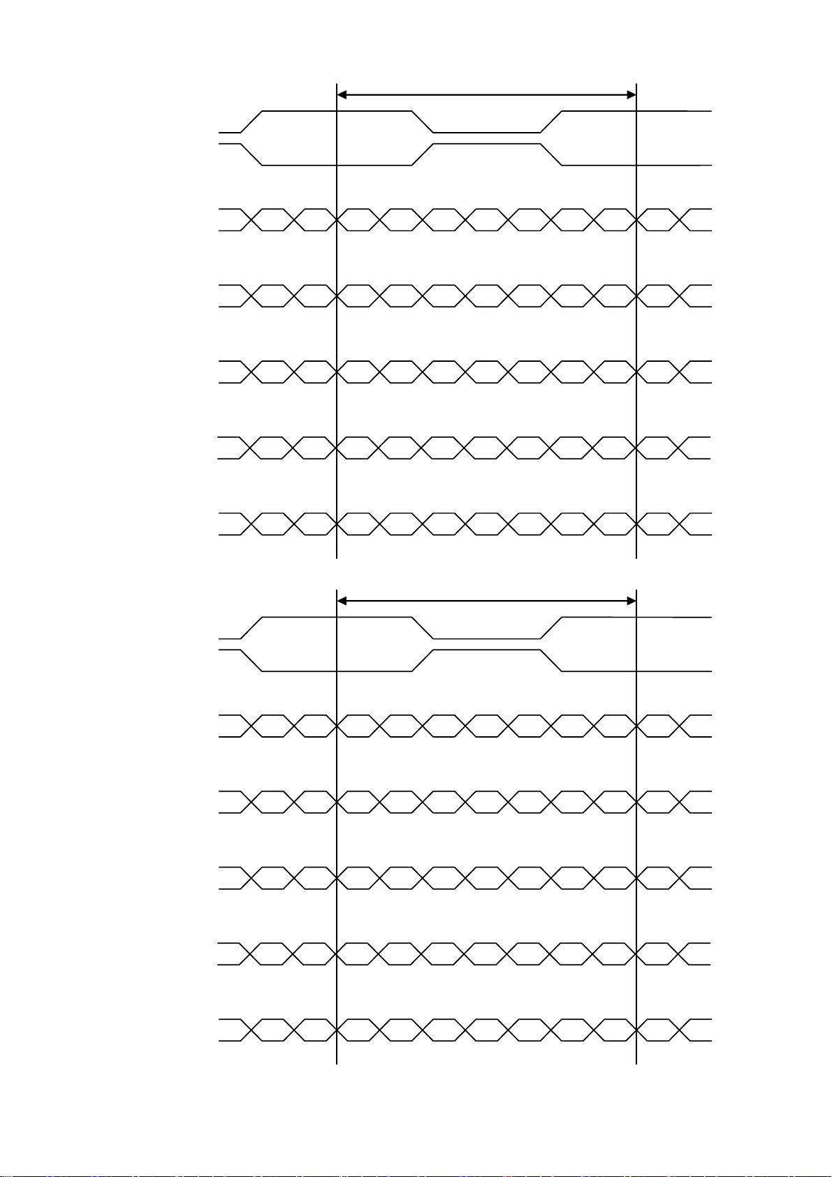
Timing diagrams of input signal are shown in Fig.2.
Parameter Symbol Min. Typ. Max. Unit Remark
Clock Frequency 1/Tc 69 74.25
Horizontal period TH
Horizontal period
Data enable
signal
[Note]-When vertical period is very long, flicker and etc. may occur.
-Please turn off the module after it shows the black screen.
-Please make sure that length of vertical period should become of an integral multiple of horizontal
length of period. Otherwise, the screen may not display properly.
-As for your final setting of driving timing, we will conduct operation check test at our side, please
inform your final setting.
(High)
Vertical period TV
Vertical period
(High)
THd
TVd 1080 1080 1080 line
542
7.3
480
1096
88.2
550
7.41
480
1125
120
76.0
600
8.1
480
1400
123.1
Icc
MHz
clock
µs
clock
line
Hz
Page 12

DE
Aport DATA
(R,G,B)
Bport DATA
(R,G,B)
Cport DATA
(R,G,B)
Dport DATA
(R,G,B)
DE
4.6
R1 G1 B1 R2 G2 B2
(1、1) (1,2)
TH
THd
1
2
1919 1919
Tc
3
4
TV
5
6
7
8 1920 1920
1 2 1080
Fig.2.Timing characteristics of input signal
Input data signal and display position on the screen
R1 G1 B1 R2 G2 B2
(1、3) (1,4)
LD-K22223A-10
1917 1917
1918 1918
1079
TVd
1・1 1・2 1・3
2・1 2・2
3・1
1080・1
1・4
R G B
Display position of Dat (V,H)
1・1920
1080・1920
[Note] Scan direction is setting for using S-PWBs’ side up. ▲A
Page 13

4.7 LVDS signal characteristics
CLK-
CLK+
RINx-
RINx+
tpd0
tpd1
t
CLK
Vdiff=0 Vdiff=0
tpd2
tpd3
tpd4
tpd5
tpd6
LD-K22223A-11
Data
position
The item Symbol min. typ. max. unit
Delay time, CLK rising
edge to serial bit position 0
Delay time, CLK rising
edge to serial bit position 1
Delay time, CLK rising
edge to serial bit position 2
Delay time, CLK rising
edge to serial bit position 3
Delay time, CLK rising
edge to serial bit position 4
Delay time, CLK rising
edge to serial bit position 5
Delay time, CLK rising
edge to serial bit position 6
tpd0
tpd1
tpd2
tpd3
tpd4
tpd5
tpd6
-0.25 0 0.25
1*t
2* t
3* t
4* t
5* t
6* t
CLK
CLK
CLK
CLK
CLK
CLK
/7-0.25 1* t
/7-0.25 2* t
/7-0.25 3* t
/7-0.25 4* t
/7-0.25 5* t
7-0.25 6* t
/7 1* t
CLK
/7 2* t
CLK
/7 3* t
CLK
/7 4* t
CLK
/7 5* t
CLK
/7 6* t
CLK
CLK
CLK
CLK
CLK
CLK
CLK
/7+0.25
/7+0.25
/7+0.25
/7+0.25
/7+0.25
/7+0.25
ns
Page 14

LD-K22223A-12
5 Optical Specifications
5.1 Input Signal, Basic Display Colors and Gray Scale of Each Color
Colors &
Gray scale
Black – 0 0 0 0 0 0 0 0 0 0 0 0 0 0 0 0 0 0 0 0 0 0 0 0 0 0 0 0 0 0
Blue – 0 0 0 0 0 0 0 0 0 0 0 0 0 0 0 0 0 0 0 0 1 1 1 1 1 1 1 1 1 1
Green – 0 0 0 0 0 0 0 0 0 0 1 1 1 1 1 1 1 1 1 1 0 0 0 0 0 0 0 0 0 0
Cyan – 0 0 0 0 0 0 0 0 0 0 1 1 1 1 1 1 1 1 1 1 1 1 1 1 1 1 1 1 1 1
Red – 1 1 1 1 1 1 1 1 1 1 0 0 0 0 0 0 0 0 0 0 0 0 0 0 0 0 0 0 0 0
Basic Color
Magenta – 1 1 1 1 1 1 1 1 1 1 0 0 0 0 0 0 0 0 0 0 1 1 1 1 1 1 1 1 1 1
Yellow – 1 1 1 1 1 1 1 1 1 1 1 1 1 1 1 1 1 1 1 1 0 0 0 0 0 0 0 0 0 0
White – 1 1 1 1 1 1 1 1 1 1 1 1 1 1 1 1 1 1 1 1 1 1 1 1 1 1 1 1 1 1
Black GS0 0 0 0 0 0 0 0 0 0 0 0 0 0 0 0 0 0 0 0 0 0 0 0 0 0 0 0 0 0 0
Gray
R0 R1 R2 R3 R4 R5 R6 R7 R8 R9 G0 G1 G2 G3 G4 G5 G6 G7 G8 G9 B0 B1 B2 B3 B4 B5 B6 B7 B8 B9
Scale
× GS1 1 0 0 0 0 0 0 0 0 0 0 0 0 0 0 0 0 0 0 0 0 0 0 0 0 0 0 0 0 0
Darker GS2 0 1 0 0 0 0 0 0 0 0 0 0 0 0 0 0 0 0 0 0 0 0 0 0 0 0 0 0 0 0
×
Ø
Brighter GS1021 1 0 1 1 1 1 1 1 1 1 0 0 0 0 0 0 0 0 0 0 0 0 0 0 0 0 0 0 0 0
↓
↓
↓
↓
Gray Scale of Red
Ø GS1022 0 1 1 1 1 1 1 1 1 1 0 0 0 0 0 0 0 0 0 0 0 0 0 0 0 0 0 0 0 0
Data signal
↓
↓
↓
↓
Red GS1023 1 1 1 1 1 1 1 1 1 1 0 0 0 0 0 0 0 0 0 0 0 0 0 0 0 0 0 0 0 0
Black GS0 0 0 0 0 0 0 0 0 0 0 0 0 0 0 0 0 0 0 0 0 0 0 0 0 0 0 0 0 0 0
× GS1 0 0 0 0 0 0 0 0 0 0 1 0 0 0 0 0 0 0 0 0 0 0 0 0 0 0 0 0 0 0
Darker GS2 0 0 0 0 0 0 0 0 0 0 0 1 0 0 0 0 0 0 0 0 0 0 0 0 0 0 0 0 0 0
×
Ø
Brighter GS1021 0 0 0 0 0 0 0 0 0 0 1 0 1 1 1 1 1 1 1 1 0 0 0 0 0 0 0 0 0 0
Gray Scale of Green
Ø GS1022 0 0 0 0 0 0 0 0 0 0 0 1 1 1 1 1 1 1 1 1 0 0 0 0 0 0 0 0 0 0
Green GS1023 0 0 0 0 0 0 0 0 0 0 1 1 1 1 1 1 1 1 1 1 0 0 0 0 0 0 0 0 0 0
Black GS0 0 0 0 0 0 0 0 0 0 0 0 0 0 0 0 0 0 0 0 0 0 0 0 0 0 0 0 0 0 0
↓
↓
↓
↓
↓
↓
↓
↓
× GS1 0 0 0 0 0 0 0 0 0 0 0 0 0 0 0 0 0 0 0 0 1 0 0 0 0 0 0 0 0 0
Darker GS2 0 0 0 0 0 0 0 0 0 0 0 0 0 0 0 0 0 0 0 0 0 1 0 0 0 0 0 0 0 0
Ø
Ø
Brighter GS1021 0 0 0 0 0 0 0 0 0 0 0 0 0 0 0 0 0 0 0 0 1 0 1 1 1 1 1 1 1 1
Gray Scale of Blue
Ø GS1022 0 0 0 0 0 0 0 0 0 0 0 0 0 0 0 0 0 0 0 0 0 1 1 1 1 1 1 1 1 1
Blue GS1023 0 0 0 0 0 0 0 0 0 0 0 0 0 0 0 0 0 0 0 0 1 1 1 1 1 1 1 1 1 1
↓
↓
↓
↓
↓
↓
↓
↓
0: Low level voltage, 1: High level voltage.
Each basic color can be displayed in 1024 gray scales from 10 bits data signals. According to the combination of
total 30 bits data signals, one billion-color display can be achieved on the screen.
Page 15
6 Optical Specifications
6.1 Optical characteristics ▲A
Parameter Symbol Condition Min. Typ. Max. Unit Remark
θ
Viewing angle
range
Contrast ratio CRn 3200 4000 - - [Note2,4]
Horizontal
Vertical
θ
θ
θ
21
22
11
12
CR>10
LD-K22223A-13
Ta=2 5°C, Vcc=12.0V, Timing:120Hz(typ. value)
70 88 - Deg.
70 88 -
Deg.
[Note1,4]
Response time
White
Red
Chromaticity
Luminance White YL 400 450 - cd/m2 [Note 4]
Luminance
uniformity
-Optical characteristics (except Note7) are based on SHARP standard module (CCFL)
-The measurement shall be executed 60 minutes after lighting at rating.
[Note]The optical characteristics are measured using the following equipment.
Fig.4-1 Measurement of viewing angle range and
Green
Blue
White
Detector(EZ-CONTRAST/ Photodiode)
Center of the screen (θ=0°)
TFT-LCD Module
Response time.
Viewing angle range: EZ-CONTRAST
Response time: Photodiode
τ
δw
DRV
x
y
x
y
x
y
x
y
θ
=0 deg.
4 ms [Note3,4,5]
Typ.-0.03 (0.270) Typ.+0.03
Typ.-0.03 (0.280) Typ.+0.03
Typ.-0.03 (0.650) Typ.+0.03
Typ.-0.03 (0.340) Typ.+0.03
Typ.-0.03 (0.282) Typ.+0.03
Typ.-0.03 (0.635) Typ.+0.03
Typ.-0.03 (0.145) Typ.+0.03
Typ.-0.03 (0.060) Typ.+0.03
- - (1.34) [Note 6,7]
Detector(SR-3A-L1)
400mm
Field=1°
Center of the screen (θ=0°)
TFT-LCD Module
Fig.4-2 Measurement of Contrast, Luminance,
-
-
-
-
-
-
-
-
[Note 4,7]
Chromaticity
.
Page 16

LD-K22223A-14
[Note 1]Definitions of viewing angle range :
Normal line
θ
11
θ
21
θ
12
θ
22
6 o’clock direction
[Note 2]Definition of contrast ratio :
The contrast ratio is defined as the following.
Luminance (brightness) with all pixels white
Contrast Ratio
=
Luminance (brightness) with all pixels black
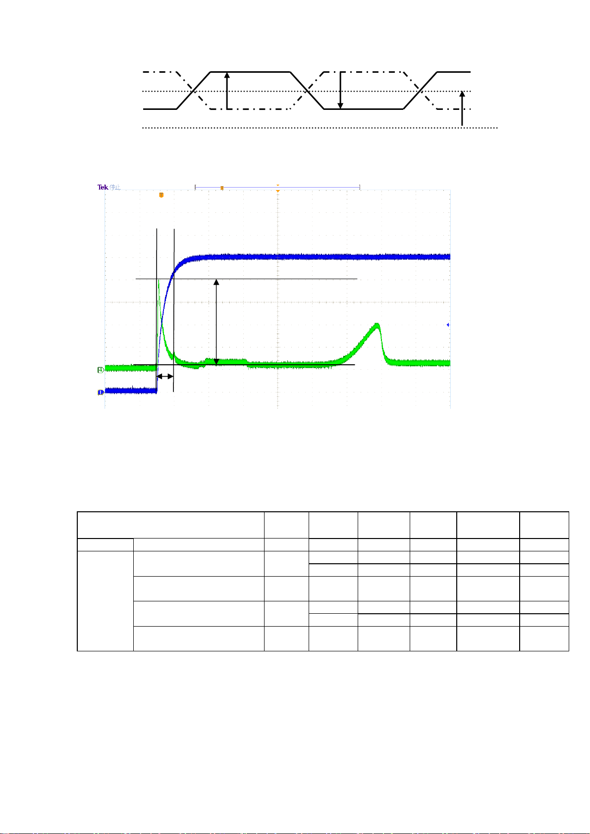
[Note 3]Definition of response time
The response time (τ
and τr) is defined as the following figure and shall be measured by switching the input
d
signal for “any level of gray (0%, 25%, 50%, 75% and 100%)” and “any level of gray (0%, 25%, 50%, 75%
and 100%)”.
0% 25% 50% 75% 100%
0%
25%
50%
75%
100%
tr: 0%-25% tr: 0%-50% tr: 0%-75% tr: 0%-100%
td: 25%-0% tr: 25%-50% tr: 25%-75% tr: 25%-100%
td: 50%-0% td: 50%-25% tr: 50%-75% tr: 50%-100%
td: 75%-0% td: 75%-25% td: 75%-50% tr: 75%-100%
td: 100%-0% td: 100%-25% td: 100%-50% td:100%-75%
t*:x-y...response time from level of gray(x) to level of gray(y)
= Σ(tr:x-y)/10 , τd = Σ(td:x-y)/10
τ
r
Bright
100%
90%
Dark
Bright
Photodetector
10%
Output
0%
τd τr
time
[Note 4]This shall be measured at center of the screen.
[Note 5] This value is valid when O/S driving is used at typical input time value.
Page 17
Y
V
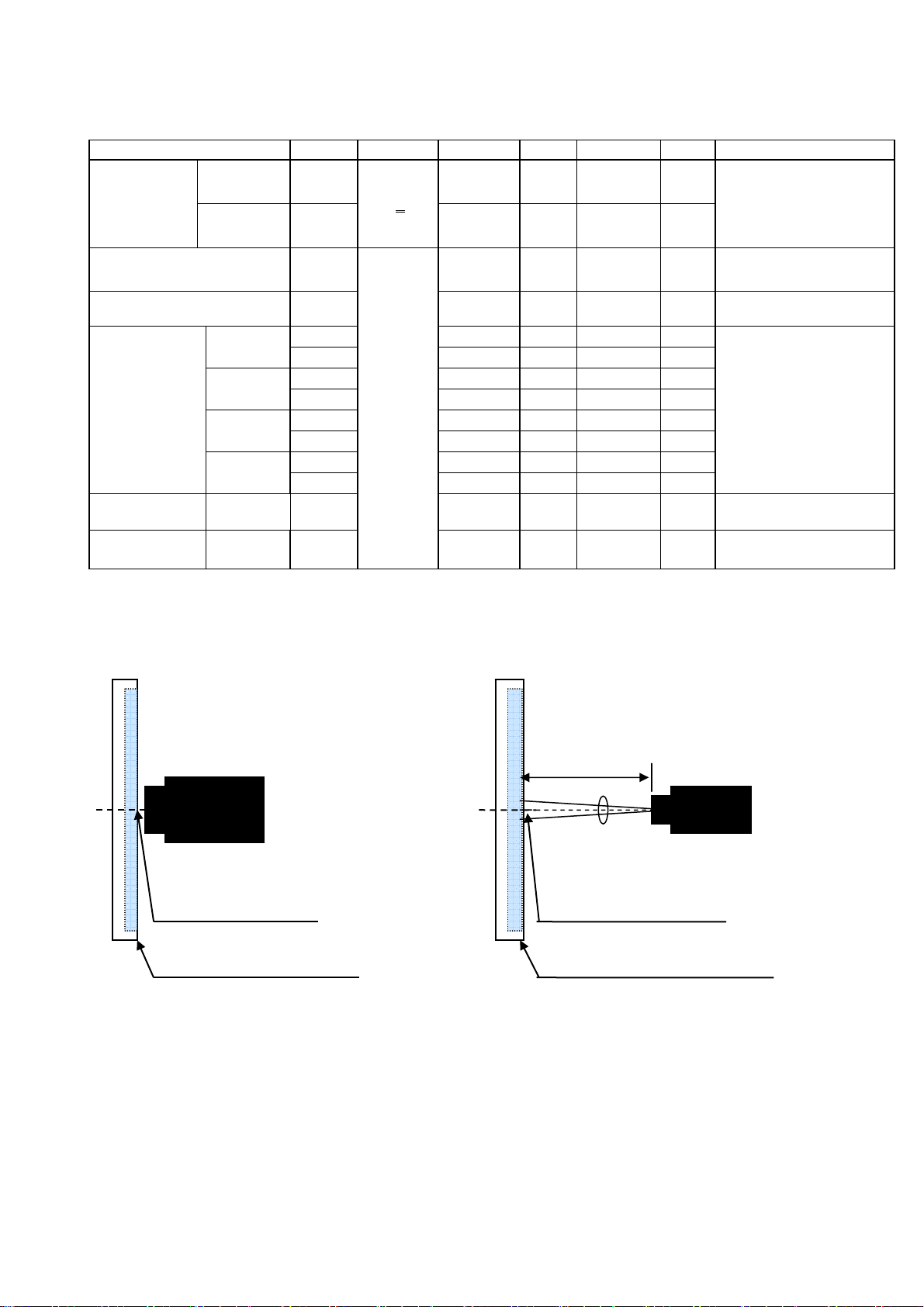
[Note 6] This value is calculated as the following with nine measurements. (1∼9) ▲A
Maximum luminance of nine points (brightness)
W=
δ
Minimum luminance of nine points (brightness)
320 960 1600
LD-K22223A-15
1
7 9
2
5
8
3
6 4
180
540
900
[pixels]
[Note7] This value is reference based on measurement result by SEC backlight system. ▲A
7 Packing for shipping
7.1 Packing form
a) Piling number of cell boxes : 14cell box/1 palette
b) Packing quantity in one cell box : 10pcs.
c) Carton size :1360(W)×1120(D)×1063(H)
d) Total mass of one carton filled with full Open Cell : 358.4kg Max
7.2 Label
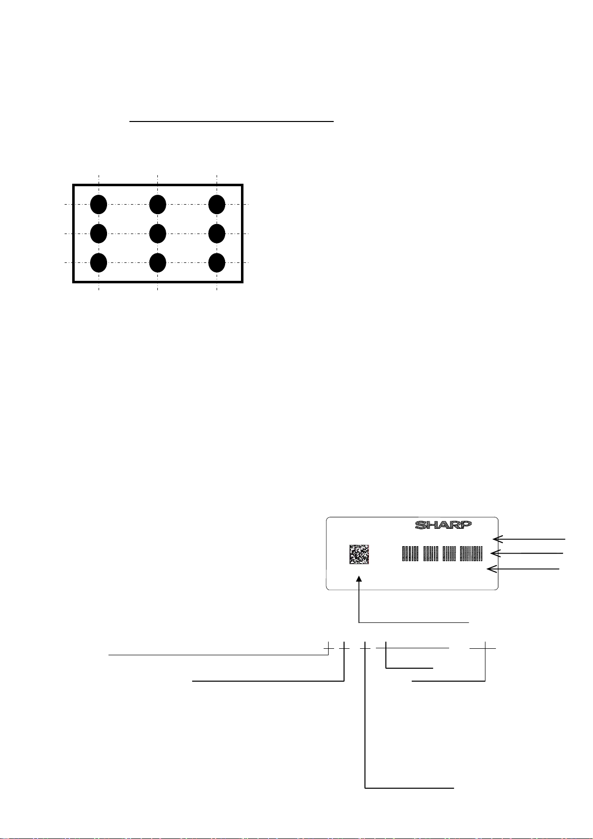
a) Open Cell Label
This label is stuck on the protection film of front polarizer.
【LK400D3HA3K】JAPAN PRODUCTION
A production year(the last figures of the Christian Era)
A production month (1-9, X,Y, Z)
LK400D3HA3K
X X K00001 *
2D Barcode
How to express Lot No.
○ ○ ○ ○ ○ ○ ○ ○ - -
Serial No.
Management No.
K: Kameyama Plant.
L: Kameyama Tec. Kameyama Fab.
N: NSEC
F: DID
: TPV
: TOT
Module No.
Barcode
Lot No.
Page 18
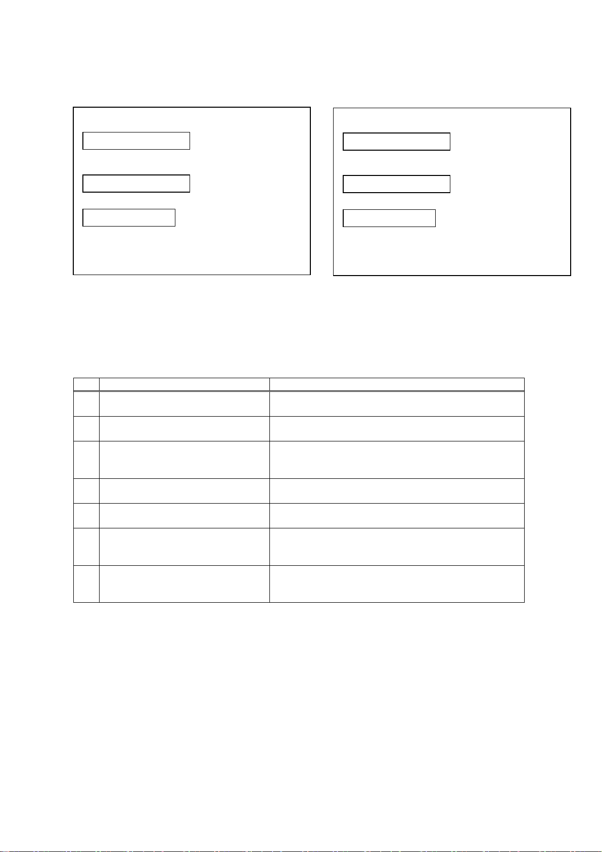
b) Packing Label
(
)
(
)
This Label is stuck on the packing case(cell box) and carton.
[LK400D3HA3K*]
b-1)Cell box b-2)Carton
【LK520D3LZ97X,T】
社内品番:
LotNO.
4S
Bar code (①)
(1T)200*. *.**
LK400D3HA3K*
社内品番:
Bar code
LotNO.
4S
LK400D3HA3K*
(①)
(1T)200*. *.**
Bar code
Quantity:
Bar code
ユーザ品番
シャープ物流用ラベルです。
(②)
(Q)
(③)
Bar code
pcs
Quantity:
Bar code
ユーザ品番
シャープ物流用ラベルです。
(②)
(Q)
(③)
① Management No.
② Lot No. (Date)
③ Quantity
8 Reliability ▲A
Reliability test item
No. Test item Condition
1
2
High temperature storage test
(Open Cell)
Low temperature storage test
(Open Cell)
High temperature and
3
high humidity operation test
Ta = 6 0
Ta = -25
Ta = 4 0
(No condensation)
(Open Cell)
4
5
High temperature operation test
(Open Cell)
Low temperature operation test
(Open Cell)
Vibration test
6
(Cell Box with full Open Cells)
Ta = 5 0
Ta = 0
X and Y direction: 15min, Z direction: 60min.
5Hz to 50Hz acceleration velocity: 1.0G
Sweeping ratio: 3min
7
(Cell Box with full Open Cells)
Drop test
Height: 25cm (corner and edge), 32cm (surface)
Number: 8times
(corner 1time and edge 3times and surface 4times)
[Result evaluation criteria]
Under the display quality test condition with normal operation state, there shall be no change,
which may affect practical display function.
o
C 240h
o
C 240h
o
C 95%RH 240h
o
C 240h
o
C 240h
LD-K22223A-16
pcs
Page 19

LD-K22223A-17
9 Handling Precautions of the Open Cell
a) Be sure to turn off the power supply when inserting or disconnecting the cable.
b) Be sure to design the LCD module and cabinet so that the Open Cell can be installed without any extra stress
such as warp or twist.
c) Since the polarizer is easily damaged, pay attention not to scratch it.
d) Since long contact with water may cause discoloration or spots, wipe off water drop immediately.
e) When the panel surface is soiled, wipe it with absorbent cotton or other soft cloth.
f) Since the panel is made of glass, it may break or crack if dropped or bumped on hard surface. Handle with
care.
g) Since a open cell consists of a TFT cell and electronic circuits with CMOS-ICs, which are very weak to
electrostatic discharge, persons who are handling a open cell should be grounded through adequate methods
such as an anti-static wrist band. Connector pins should not be touched directly with bare hands.
・Reference : Process control standard of sharp
item Management standard value and performance standard
1 Anti-static mat(shelf) 1 to 50 [Mega ohm]
2 Anti-static mat(floor,desk) 1 to 100 [Mega ohm]
3 Ionizer Attenuate from ±1000V to ±100V within two seconds.
4 Anti-static wrist band 0.8 to 10 [Mega ohm]
5 Anti-static wrist band entry and
ground resistance
6 Temperature 22 to 26 [oC]
7 Humidity 60 to 70 [%RH]
h) The Open Cell has some PWBs, take care to keep them form any stress or pressure when handling or
installing the Open Cell; otherwise some of electronic parts on the PWBs may be damaged.
i) When handling LCD modules and assembling them into cabinets, please be noted that long-term storage in
the environment of oxidization or deoxidization gas and the use of such materials as reagent, solvent,
adhesive, resin, etc. which generate these gasses, may cause corrosion and discoloration of the LCD Open
Cell.
j) Observe all other precautionary requirements in handling components.
k) Applying too much force and stress to PWB and SOF may cause a malfunction electrically and
mechanically.
l) The TFT open cell has high frequency circuits. Sufficient suppression to EMI should be done by system
manufacturers.
m) When you peel the protection film for a polarizer.
・The protection film should be peeled as Fig.3
・Slowly(Recommendation : more than 5[sec]) & constant speed
・Persons who are electrically grounded with adequate methods such as an anti-static wrist band.
・Ionized air should be blown over the during peeling action..
・Ground S-PWB connectors while peeling of a protection film.
・The protection film must not touch SOFs.
Below 1000 [ohm]
Fig.3 Direction peeled off
Page 20

LD-K22223A-18
・Please remove with isopropyl-alcohol if adhesive may remain on a polarizer after a protection film is peeled
off.
n) Electrical components which may not affect electrical performance are subjective to change without notice
because of their availability.
o) Please be careful since image retention may occur when a fixed pattern is displayed for a long time.
p) The chemical compound, which causes the destruction of ozone layer, is not being used.
q) This Open Cell is corresponded to RoHS. ‘‘R.C.’’ label on the side of palette shows it.
r) When any question or issue occurs, it shall be solved by mutual discussion.
10 Carton storage condition.
Temperature 0°C to 40°C
Humidity 95%RH or less
Reference condition : 20°C to 35°C, 85%RH or less (summer)
: 5°C to 15°C, 85%RH or less (winter)
· the total storage time (40°C, 95%RH) : 240H or less
Sunlight Be sure to shelter a product from the direct sunlight.
Atmosphere Harmful gas, such as acid and alkali which bites electronic components and/or
wires must not be detected.
Notes Be sure to put cartons on palette or base, don’t put it on floor, and store them with
removing from wall
Please take care of ventilation in storehouse and around cartons, and control
changing temperature is within limits of natural environment
Storage life 1 year
Page 21

Page 22

 Loading...