

Page 1
T315XW01 VH (QD32HL05) 1of 32
Product Description:
AUO Model Name: T315XW01 VH (QD32HL05 Rev.01)
Customer Part No/Project Name: LK315T3LF12
Customer Signature Date AUO Date
Approved By: Frank Ko
Reviewed By: HongJye Hong
Prepared By: CT Wu
©Copyright AU Optronics, Inc.
January, 2006 All Rights Reserved. T315XW01 VH - Specs. Ver 05 1/35
Page 2

T315XW01 VH (QD32HL05) 2of 32
Document Version : 05
Date : 200611/02
Product Specifications
31.5” WXGA Color TFT-LCD Module
Model Name: T315XW01 VH
(QD32HL05 Rev.01)
( ) Preliminary Specifications
(*) Final Specifications
©Copyright AU Optronics, Inc.
January, 2006 All Rights Reserved. T315XW01 VH - Specs. Ver 05 2/35
Page 3

T315XW01 VH (QD32HL05) 3of 32
These specification sheets are the proprietary product of AUO Optronics Inc. (”AUO”)
and include materials protected under copyright of AUO. Do not reproduce or cause any
third party to reproduce them in any form or by any means, electronic or mechanical, for
any purpose, in whole or in part, without the express written permission of AUO.
The device listed in these technical literature sheets was designed and manufactured for
use in OA equipment.
In case of using the device for applications such as control and safety equipment for
transportation (aircraft, trains, automobiles, etc.), rescue and security equipment and
various safety related equipment which require higher reliability and safety, take into
consideration that appropriate measures such as fail-safe functions and redundant system
design should be taken.
Do not use the device for equipment that requires an extreme level of reliability, such as
aerospace applications, telecommunication equipment (trunk lines), nuclear power control
equipment and medical or other equipment for life support.
AUO assumes no responsibility for any damage resulting from the use of the device, which
does not comply with the instructions, and the precautions specified in these technical
literature sheets.
Contact and consult with an AUO sales representative for any questions about this device.
©Copyright AU Optronics, Inc.
January, 2006 All Rights Reserved. T315XW01 VH - Specs. Ver 05 3/35
Page 4
T315XW01 VH (QD32HL05) 4of 32
Revision History
Ver.
01 Dec. 13,2005
02 Jan.11,2006
03 Jan.13,2006
Date ECN NO. Change Content
NA Preliminary Specification Initiate
1.Updated haze, connector (Page: 5, 6, 8)
2.Updated electrical characteristics (Page: 10, 11).
NA
NA
3.Updated optical characteristics (Page: 17).
4.Updated module Reliability test item ESD: C&R (Page: 20).
5,Updated modue label, packing label (Page: 20).
1.Updated Vcc-dip conditions: 4V ≦ Vcc <4.5 V (Page: 11)
2.Update 7-1. Timing characteristics (Page: 15).
9. Optical characteristic (page18)
Add Note 4
03 Jan.14,2006
NA
12.Reliability test items (page 21)
Change item name to “High temperature storage test 2”
Add item 16 (Page 31 and 32)
1.Updated input voltage for control 5.5V (Page 10)
2.Updated rush current spec.: 3.0A (max.) (Page 11).
3.Updated backlight driving characteristics and lamp life time (typ.) to
60000hrs (Page 12).
4.Updated timing characteristics F
(Page 15).
04 Mar.04, 2006
05 Nov.02, 2006
NA
CECN-31T01-
0610-01
5.Added remark V
6.Changed reliability test item and criteria (item10) name to “High
temperature operation test2”, proceeded in operation mode (Page:21, 31).
7.Correct reliability test ESD C&R condition, 150PF/330Ω(Page: 21, 30).
8.Updated Lot No. label and packing label description (Page:22, 23)
9.Updated module back view drawing with FFC protect Mylar modification
(Page 25).
1. Update Produce spec document format to AUO standard.
2. Update AUO model name QD32HL05 Rev01 à T315XW01 VH
3. Update Serial label & carton label format. (page 23)
(max.): 82MHz changed to 85MHz
CLK
=3.3V at luminance of white (Page 18).
BRTC
©Copyright AU Optronics, Inc.
January, 2006 All Rights Reserved. T315XW01 VH - Specs. Ver 05 4/35
Page 5

T315XW01 VH (QD32HL05) 5of 32
Content List
Page
1. Application 6
2. Overview 6
3. General Specifications 6
4. Input Terminals 7
5. Absolute Maximum Ratings 11
6. Electrical Characteristics 12
7. Timing Characteristics of LCD module input signals 16
8. Input Signals, Basic Display Colors and Gray
Scale of Each Color 18
9. Optical Characteristics 19
10. Display Quality 21
11. Handling Precautions 21
12. Reliability Test Items 22
13. Others (Label & Pallet packing) 23
14. Drawing 25
15. Packing 27
16. Reliability test criteria 31
©Copyright AU Optronics, Inc.
January, 2006 All Rights Reserved. T315XW01 VH - Specs. Ver 05 5/35
Page 6
T315XW01 VH (QD32HL05) 6of 32
1. Application
This specification applies to a color TFT-LCD module, QD32HL05
2. Overview
This module is a color active matrix LCD module incorporating amorphous silicon
TFT (Thin Film Transistor). It is composed of a color TFT-LCD panel; driver ICs, control
circuit and power supply circuit and a backlight unit. Graphics and texts can be displayed
on a 1366×3×768 dots panel with 16.7 million colors by using the LVDS (Low Voltage
Differential Signaling) interface, 8-bit driving method and supplying +5V DC supply
voltage for TFT-LCD panel driving.
The TFT-LCD panel used for this module has fast response time. A low-reflection
and higher-color-saturation type color filter is also used for this panel. Therefore,
high-brightness and high-contrast image, which is suitable for multimedia use, can be
obtained by using this module.
[Features]
1) High aperture panel; high brightness
2) Brilliant and high contrast image
3) High speed response
4) WXGA resolution, 16:9
5) LVDS interface
6) QSV technology
7) Wide viewing angle
3. General Specifications
Parameter Specifications Unit
Display size 80.04 (31.51") Diagonal cm
Active area
Pixel format
697.685 (H)×392.256 (V)
1366 (H)×768 (V)
mm
Pixel
(1 pixel = R+G+B dots)
Pixel pitch
0.5107(H) × 0.5107 (V)
mm
Pixel configuration R,G, B vertical stripe
Display mode Normally Black
Unit outline dimensions
760 (W)×450 (H)×48(D)
mm
Thickness 48 max. mm
Weight 7000 max. g
Surface treatment Anti-glare (Haze 13 %) and
hard-coating 3H
Lamp Quantity 16 straight lamps pcs
©Copyright AU Optronics, Inc.
January, 2006 All Rights Reserved. T315XW01 VH - Specs. Ver 05 6/35
Page 7
T315XW01 VH (QD32HL05) 7of 32
4. Input Terminals
4-1. TFT-LCD pin assignment of panel
CN1: FI-X30SSL-HF (JAE) or equivalent
Pin NO.
1
2
3
4
5
6
7
8
VCC +5V input
VCC +5V input
VCC +5V input
VCC +5V input
GND Power Ground
GND Power Ground
GND Power Ground
GND Power Ground
Symbol Function Remark
LVDS data mapping
9 LVDS SELECT
Low/Open for Normal
(NS),
High for JEIDA
10
11
12
13
14
15
16
17
18
19
20
21
22
23
24
25
26
27
RESERVED N.C.
GND Ground
RXIN0- LVDS data input
RXIN0+ LVDS data input
GND Ground
RXIN1- LVDS data input
RXIN1+ LVDS data input
GND Ground
RXIN2- LVDS data input
RXIN2+ LVDS data input
GND Ground
RXCLK- LVDS clock input
RXCLK+ LVDS clock input
GND Ground
RXIN3- LVDS data input
RXIN3+ LVDS data input
GND Ground
RESERVED N.C.
Low: 0-0.8 V;
High: 2.7-3.3 V;
Default NS type.
Low/Open for
PAL(50Hz)
High for NTSC(60Hz)
28
29
30
NTSC or
_PAL_SELECTION
OD table selection
GND Ground
GND Ground
【
Note 1】All GND(ground) pins should be connected together and to VCC which should
also be connected to the LCDs metal frame.
【
Note 2】Relation between LVDS signals and actual data shows below section (7-1).
©Copyright AU Optronics, Inc.
January, 2006 All Rights Reserved. T315XW01 VH - Specs. Ver 05 7/35
Page 8
T315XW01 VH (QD32HL05) 8of 32
R4 R3 R2 G2 R7 R6 R5 R4 R3 R2
G5 G4 G3 B3 B2 G7 G6 G5 G4 G3
B6 B5 B4 DE VS HS B7 B6 B5 B4 G0 R1 R0 -- B1 B0 G1 G0 R1 R0 G2
B3
DE --
R2 R1 R0 G0 R5 R4 R3 R2 R1 R0 G3 G2 G1 B1 B0 G5 G4 G3 G2 G1
B4 B3 B2 DE VS HS B5 B4 B3 B2 G6 R7 R6 -- B7 B6 G7 G6 R7 R6
G0 B1
DE --
【
Note 3】All VCC (power supply) pins should be connected together.
LVDS OPTION=High(3.3 V)
RXCLK-/+
RXIN0-/+
RXIN1-/+
RXIN2-/+
RXIN3-/+
LVDS OPTION=LOW (GND)/ NC
RXCLK-/+
RXIN0-/+
RXIN1-/+
RXIN2-/+
RXIN3-/+
©Copyright AU Optronics, Inc.
January, 2006 All Rights Reserved. T315XW01 VH - Specs. Ver 05 8/35
Page 9
T315XW01 VH (QD32HL05) 9of 32
RxClk-
RxClk+
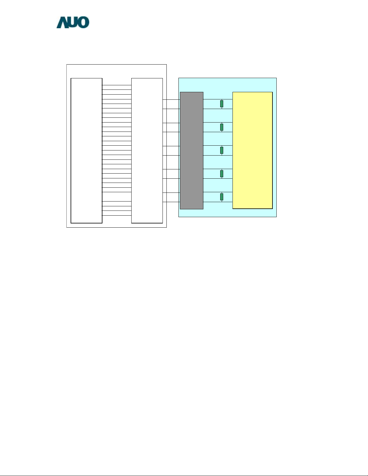
4-2 Interface block diagram
Host System 24Bit
R0
R1
R2
R3
R4
R5
R6
R7
G0
G1
G2
G3
G4
G5
G6
G7
B0
B1
B2
B3
B4
B5
B6
B7
HS
VS
DE
CLK
THC63LVDM83R
or Compatible
51
52
54
55
Tx056
3
Tx0+
50
2
4
Tx16
7
Tx1+
11
12
14
Tx28
10
Tx2+
15
19
20
TxClk22
23
TxClk+
24
16
18
Tx3-
27
Tx3+
28
30
31
48
47
46
45
42
41
40
39
38
37
LCD Module
12
12
13
13
15
15
16
16
18
18
19
19
Input
Connector
21
21
22
22
24
24
25
25
100
100
100
100
100
Rx0-
Rx0+
Rx1-
Rx1+
Rx2-
Rx2+
Rx3-
Rx3+
Timing
Controller
©Copyright AU Optronics, Inc.
January, 2006 All Rights Reserved. T315XW01 VH - Specs. Ver 05 9/35
Page 10
T315XW01 VH (QD32HL05) 10of 32
4-3. Backlight driving
4-3-1. Inverter conector
Connector
CN1
CN2~CN9
CN10
S14 B-PH-SM3 TB (JST) or Equivalent
SM02(12B)-BHS-1-TB (JST) or Equivalent
S2B-ZR-SM3A-TF (JST) or Equivalent
Type
4-3-2 Pin assignment of inverter (CN1)
Pin
Symbol Description Remark
No.
1 VDD +24V DC
2 VDD +24V DC
3 VDD +24V DC
4 VDD +24V DC
5 VDD +24V DC
6 GND Ground
7 GND Ground
8 GND Ground
9 GND Ground
10 GND Ground
11 NC Non Connection
12 BRTC Backlight On/OFF signal On : High, Off : Low
13 BRTI Luminance controlled by voltage method
Note.1
14 SGND Signal Ground
Note.1 Luminance ratio is linearly controllable in the range of the following table.
BRTI Voltage (VBI) Luminance ratio
0V 20% (Minimum)
3.3V 100% (Maximum)
©Copyright AU Optronics, Inc.
January, 2006 All Rights Reserved. T315XW01 VH - Specs. Ver 05 10/35
Page 11

T315XW01 VH (QD32HL05) 11of 32
℃
5. Absolute Maximum Ratings
LCD module
Parameter Symbol Condition
Input Voltage (for control) VI
5 V Supply Voltage (for Pannel) VCC
Input Voltage (for inverter) V
24V supply voltage (for Inverter) V
Storage temperature
brt
INV
Tstg
Ta=25℃
Ta=25℃ 0 ~ +6.0
Ta=25
Ta=25
Operating temperature (Ambient) Topa
【
Note1】LVDS SELECT, NTSC or PAL SELECTION
【
Note2】BRTC,BRTI
【
Note3】Humidity:90%RH Max. at Ta≦40℃.
℃
℃
-
-20 ~ +60
-
0 ~ +50
Ratings Unit Remark
-0.3 ~ +5.5
0 ~ +6.0
0 ~ 27.5
V
V
V
V
DC
DC
DC
DC
【
【
【
Note1
Note2
Note3
℃
Maximum wet-bulb temperature at 39℃ or less at Ta>40℃.
No condensation.
】
】
】
©Copyright AU Optronics, Inc.
January, 2006 All Rights Reserved. T315XW01 VH - Specs. Ver 05 11/35
Page 12

T315XW01 VH (QD32HL05) 12of 32
90 %
10 %
T2 T3 T4 T5 T6 T7
Vi (Parallel CMOS Signal)
6. Electrical Characteristics
6-1TFT-LCD panel driving Ta=25 C
Vcc
Parameter Symbol Min. Typ. Max. Unit
Supply input voltage Vcc +4.5 +5 +5.5
Supply input current ICQ
Power description PD
-
-
960 1400 mA
4.8 7.7 W
V
Remark
【
Note2】
【
Note3】
Rush current Iccs 3.0 A
Permissive Input Ripple
Vrp 120 mV
Voltage
Differential input High
Threshold voltage Low
LVDS select (High)
LVDS select (Low)
Input current (High)
Input current (Low)
Terminal resistor
【
Note1】VCM : Common mode voltage of LVDS driver.
【
Note2】On-off conditions for supply voltage
Power Supply For LCD
Vcc
10 %
VTH
VTL
VIH
VIL
IOH
IOL
RT
90 %
-
–100
-
-
+100 mV VCM=+1.2V
-
mV
2.7 3.3 V
0 0.8 V
-
-
-
-
-
100
+/-10
+/-10
-
μ
A
μ
A
Ω
【
Note1】
VI=3.3V
VI=0V
Differential input
0
Interface Signal.
T1
Valid
0
Power For Lamp
0F
0<T1≦10ms; 0.5ms<T2≦50ms; 200ms≦T3; 200ms≦T4; 0.5ms<T5≦50ms; 0<T6
Lamp
0F
≦
10ms; 400ms<T7
Vcc
Vcc-dip conditions
1) 4V ≦ Vcc <4.5V
4V
4.5V
td ≦10 ms
2) V
Vcc-dip conditions should also follow the On-off conditions for supply voltage
cc
<
4 V
t
d
©Copyright AU Optronics, Inc.
January, 2006 All Rights Reserved. T315XW01 VH - Specs. Ver 05 12/35
Page 13

T315XW01 VH (QD32HL05) 13of 32
【Note3】
Typical current condition: 2-line vertical stripe pattern (0,255GS). VCC=+5V
BR G
BR G
BR G
BR G
BR G
BR G
BR G
BR G
BR G
BR G
BR G
BR G
BR G
BR G
BR G
BR G
BR G
BR G
BR G
BR G
BR G
BR G
BR G
BR G
BR G
BR G
BR G
BR G
BR G
BR G
Max current condition: 1x1dot Checker Board Pattern (0, 255GS). VCC=+5V
R G B R G B
R G B R G B
R G B R G B
R G B R G B
:0 GS
:255 GS
6-2. Backlight driving
The backlight system is a direct-lighting type with 16 CCFT (Cold Cathode
Fluorescent Tube).
The characteristics of the lamp are shown in the following table.
Parameter Symbol Min. Typ. Max. Unit
Remark
BR G
BR G
BR G
BR G
BR G
BR G
Power Supply Input Voltage V
Power Supply Input Current
Power Consumption P
DD
IDD 4.1 4.6 5.0 A
DD
Lamp current IL 4.5 5.0 5.5 mA
Lamp voltage V L 1215 1350 1485 Vrms
Lamp power consumption
PL - 6.75 8.17
21.6 24.0 26.4 V
- 110.4 132 W
W
【Note1】
【Note3】
【Note2】
±
10%
by per lamp
Ripple Voltage Vrf - - 800 mV
Diming Voltage VBrt 0 - 3.3 V Input Impedance:58K
BRTC(ON / OFF Voltage)
Lamp frequency FL 56 58 60 kHz
Established starting voltage Vs
VON 2.0 3.3 5.0 V High
V
0 - 0.8 V Low
OFF
【
Note4】
- - 1700 Vrms Ta=25
℃
【
Note5
】
1900 Vrms Ta=0℃
Lamp life time LL 50000 60000
Hours IL<=6.0mA【Note6
】
©Copyright AU Optronics, Inc.
January, 2006 All Rights Reserved. T315XW01 VH - Specs. Ver 05 13/35
Page 14

T315XW01 VH (QD32HL05) 14of 32
【
Note1】
1. Power ON sequence:
0.9V
DD
V
DD
V
ON
T1T2
0V
2. Power OFF sequence:
V
ON
4mS < T1 ≦ 20mS
2mS ≦ T2
2mS ≦ t1
V
DD
1.0V
t1
0.9V
DD
0V
0V
©Copyright AU Optronics, Inc.
January, 2006 All Rights Reserved. T315XW01 VH - Specs. Ver 05 14/35
Page 15

T315XW01 VH (QD32HL05) 15of 32
CN10
Input
【
Note2】 Lamp current is measured with current meter at low voltage end as shown
below.
1P
CN1
14P
CN2 ~CN9
CCFL
【
Note3】 Calculated Value for reference ( I
【
Note4】 Lamp frequency may produce interference with horizontal synchronous
DD × VDD)
frequency, and this may cause beat on the display. Therefore lamp frequency
shall be detached as much as possible from the horizontal synchronous
frequency and from the harmonics of horizontal synchronous to avoid
interference.
【
Note5】 The voltage above this value should be applied to the lamp for more than 1
second to start-up. Otherwise the lamp may not be turned on.
【
Note6】Lamp life time is defined as the time when either ① or ② occurs in the
continuous operation under the condition of Ta = 25℃ and I
≦
6.0mArms.
L
① Brightness becomes 50 % of the original value under standard condition.
② Kick-off voltage at Ta = 0℃ exceeds maximum value.
©Copyright AU Optronics, Inc.
January, 2006 All Rights Reserved. T315XW01 VH - Specs. Ver 05 15/35
Page 16

T315XW01 VH (QD32HL05) 16of 32
A D E F
7. Timing characteristics of LCD module input signals
7-1. Timing characteristics
Symbol Min Typ Max Unit Notes
ITIME
Hsync
Vsync
Frequency F
Period t
Period t
Width-Active t
Frequency f
Period t
Width-Active t
CLK
CLK
HA
HC
H
VA
VC
55 80 85 MHz DCLK
18.18 12.5 - ns
1512 1648 1780 t
CLK
(A)
8 16 - (C)
36.38 48.6 52 kHz
774 810 - (A)
2 6 -
tHA
(C)
Frequency fv 47 60 63 Hz
Data
Enable
Horizontal back
porch
Horizontal front
t
HD
tHF 130 186 - t
8 80 - t
CLK
CLK
(D)
(F)
porch
Horizontal active t
Horizontal blanking t
Vertical back porch t
HE
HB
VD
1366 1366 1366 t
146 282 t
2 20 - t
CLK
CLK
HA
(E)
(B)
(D)
Vertical front porch tVF 2 16 - tHA (F)
Vertical active t
768 768 768 tHA (E)
VE
Vertical blanking tVB 6 42 tHA (B)
Notes:
1. The performance of electro-optical characteristics may be influenced by variance of the
vertical refresh rates.
2. This module is drived by the data enable signal.
The data enable signal should follow Vsync and Hsync of above table.
7-2 Signal Timing Waveform
Data
ENAB
Sync
B
C
©Copyright AU Optronics, Inc.
January, 2006 All Rights Reserved. T315XW01 VH - Specs. Ver 05 16/35
Page 17

T315XW01 VH (QD32HL05) 17of 32
7-3. Input Data Signals and Display Position on the screen
©Copyright AU Optronics, Inc.
January, 2006 All Rights Reserved. T315XW01 VH - Specs. Ver 05 17/35
Page 18

8. Input Signals, Basic Display Colors and Gray Scale of Each Color
Colors &
Gray
scale
Black
T315XW01 VH (QD32HL05) 18of 32
Data signal
Gray
Scale
R0 R1 R2 R3 R4 R5 R6 R7 G0 G1 G2 G3 G4 G5 G6 G7 B0 B1 B2 B3 B4 B5 B6 B7
-
0 0 0 0 0 0 0 0 0 0 0 0 0 0 0 0 0 0 0 0 0 0 0 0
Blue
Basic Color Gray Scale of Red Gray Scale of Green Gray Scale of Blue
Green
Cyan
Red
Magenta
Yellow
White
Black GS0 0 0 0 0 0 0 0 0 0 0 0 0 0 0 0 0 0 0 0 0 0 0 0 0
Darker GS2 0 1 0 0 0 0 0 0 0 0 0 0 0 0 0 0 0 0 0 0 0 0 0 0
Brighter GS253 1 0 1 1 1 1 1 1 0 0 0 0 0 0 0 0 0 0 0 0 0 0 0 0
Red GS255 1 1 1 1 1 1 1 1 0 0 0 0 0 0 0 0 0 0 0 0 0 0 0 0
Black GS0 0 0 0 0 0 0 0 0 0 0 0 0 0 0 0 0 0 0 0 0 0 0 0 0
Darker GS2 0 0 0 0 0 0 0 0 0 1 0 0 0 0 0 0 0 0 0 0 0 0 0 0
Brighter GS253 0 0 0 0 0 0 0 0 1 0 1 1 1 1 1 1 0 0 0 0 0 0 0 0
Green GS255 0 0 0 0 0 0 0 0 1 1 1 1 1 1 1 1 0 0 0 0 0 0 0 0
ñ
ñ
ò
ò
ñ
ñ
ò
ò
-
-
-
-
-
-
-
GS1 1 0 0 0 0 0 0 0 0 0 0 0 0 0 0 0 0 0 0 0 0 0 0 0
â
â
GS254 0 1 1 1 1 1 1 1 0 0 0 0 0 0 0 0 0 0 0 0 0 0 0 0
GS1 0 0 0 0 0 0 0 0 1 0 0 0 0 0 0 0 0 0 0 0 0 0 0 0
â
â
GS254 0 0 0 0 0 0 0 0 0 1 1 1 1 1 1 1 0 0 0 0 0 0 0 0
0 0 0 0 0 0 0 0 0 0 0 0 0 0 0 0 1 1 1 1 1 1 1 1
0 0 0 0 0 0 0 0 1 1 1 1 1 1 1 1 0 0 0 0 0 0 0 0
0 0 0 0 0 0 0 0 1 1 1 1 1 1 1 1 1 1 1 1 1 1 1 1
1 1 1 1 1 1 1 1 0 0 0 0 0 0 0 0 0 0 0 0 0 0 0 0
1 1 1 1 1 1 1 1 0 0 0 0 0 0 0 0 1 1 1 1 1 1 1 1
1 1 1 1 1 1 1 1 1 1 1 1 1 1 1 1 0 0 0 0 0 0 0 0
1 1 1 1 1 1 1 1 1 1 1 1 1 1 1 1 1 1 1 1 1 1 1 1
â
â
â
â
â
â
Black GS0 0 0 0 0 0 0 0 0 0 0 0 0 0 0 0 0 0 0 0 0 0 0 0 0
Darker GS2 0 0 0 0 0 0 0 0 0 0 0 0 0 0 0 0 0 1 0 0 0 0 0 0
Brighter GS253 0 0 0 0 0 0 0 0 0 0 0 0 0 0 0 0 1 0 1 1 1 1 1 1
Blue GS255 0 0 0 0 0 0 0 0 0 0 0 0 0 0 0 0 1 1 1 1 1 1 1 1
ñ
ñ
ò
ò
0: Low level voltage, 1: High level voltage
Each basic color can be displayed in 256 gray scales from 8 bit data signals. According to the combination of
total 24 bit data signals, the 16,777,216-color display can be achieved on the screen.
©Copyright AU Optronics, Inc.
January, 2006 All Rights Reserved. T315XW01 VH - Specs. Ver 05 18/35
GS1 0 0 0 0 0 0 0 0 0 0 0 0 0 0 0 0 1 0 0 0 0 0 0 0
â
â
GS254 0 0 0 0 0 0 0 0 0 0 0 0 0 0 0 0 0 1 1 1 1 1 1 1
Page 19

T315XW01 VH (QD32HL05) 19of 32
Photo detector
o
9. Optical Characteristics
Parameter Symbol Condition Min. Typ. Max. Unit Remark
Viewing
angle U
range
Contrast ratio
Response time
Rise time
Fall time
Gray to gary reponse time
Chromaticity of Wx 0.247 0.277 0.307
White (CIE 1931) Wy 0.257 0.287 0.317
L/R
D
τr
τd
θ21,θ
22
θ11
θ12
CRn θ=0°
τ
CR>10 80 88 Deg.
80 88 Deg.
80 88 Deg.
900 1200
TBD TBD ms
TBD TBD ms
8 TBD ms
-
TBD TBD ms
-
Ta=25℃, Vcc=+5V
【Note1,4】
【Note2,4】
【Note3,4】
【Note4】
Chromaticity of Rx 0.611 0.641 0.671
Red (CIE 1931) Ry 0.310 0.340 0.370
Chromaticity of Gx 0.254 0.284 0.314
Green (CIE 1931) Gy 0.582 0.612 0.642
Chromaticity of Bx 0.116 0.146 0.176
Blue (CIE 1931) By 0.047 0.077 0.107
Luminance of white
White Uniformity
Color Temperatore CT 10500
The measurement shall be executed 30 minutes after
※
Arms)
YL
δW
(5P)
400 500 Cd/m
-
- 1.25
ghting at rating.(Typical IL =6.0 m
li
NTSC 72%
2
V
=3.3V
BRTC
【Note4】
【Note5】
°
K
The optical characteristics shall be measured in a dark room or equivalent state with the method
shown in Fig.3 below.
(TOPCON: SR-3)
Fig 1. Optical characteristics measurement method
©Copyright AU Optronics, Inc.
January, 2006 All Rights Reserved. T315XW01 VH - Specs. Ver 05 19/35
Page 20

T315XW01 VH (QD32HL05) 20of 32
time
τrτ
d
Black
Black
White
0%
10%
100%
90%
【Note1】Definitions of viewing angle range:
【Note2】Definition of contrast ratio:
The contrast ratio is defined as the following.
Contrast Ratio (CR) =
Luminance (brightness) with all pixels white
Luminance (brightness) with all pixels black
【Note3】Definition of response time:
The response time is defined as the following figure and shall be measured by
switching the input signal for "black" and "white" .
(Relative Value)
Photo detector Output
【Note4】This shall be measured at center of the screen.
Share of module quantity of luminance over 460cd/m2; ≧ 90%
©Copyright AU Optronics, Inc.
January, 2006 All Rights Reserved. T315XW01 VH - Specs. Ver 05 20/35
Page 21

T315XW01 VH (QD32HL05) 21of 32
A C
【Note5】Definition of white uniformity:
White uniformity is defined as the following the number of measurement points
within active area, formula are δw(5)(A~E). HxV : active area
H/4
H/2
3H/4
D
V/4
V/2
B
E
3V/4
δw =
Maximum Luminance (of 5 points measurement)
Minnum Luminance (of 5 points measurement)
10. Display Quality
The display quality of the color TFT-LCD module shall be in compliance with the
Incoming Inspection Standard.
11.Handling Precautions
a) Be sure to turn off the power supply when inserting or disconnecting the cable.
b) Be sure to design the cabinet so that the module can be installed without any extra
stress such as warp or twist.
c) Since the front polarizer is easily damaged, pay attention not to scratch it.
d) Wipe off water drop immediately. Long contact with water may cause discolora
-tion or spots.
e) When the panel surface is soiled, wipe it with absorbent cotton or other soft cloth.
f) Since the panel is made of glass, it may break or crack if dropped or bumped on
hard surface. Handle with care.
g) Since CMOS LSI is used in this module, take care of static electricity and injure
the human earth when handling.
h) Observe all other precautionary requirements in handling components.
i) This module has its circuitry PCBs on the rear side and should be handled carefully
in order not to be stressed.
j) Laminated film is attached to the module surface to prevent it from being
scratched. Peel the film off slowly just before the use with strict attention to
electrostatic charges. Ionized air shall be blown over during the action. Blow off
the 'dust' on the polarizer by using an ionized nitrogen gun, etc…
©Copyright AU Optronics, Inc.
January, 2006 All Rights Reserved. T315XW01 VH - Specs. Ver 05 21/35
Page 22

T315XW01 VH (QD32HL05) 22of 32
12. Reliability test items
No. Test item Conditions
1 High temperature storage test
2 Low temperature storage test
Ta = 60℃, 500h
Ta = -25℃, 500h
3 High temperature
& High humidity operation
Ta = 40℃, 95 %RH, 500h
test
4 High temperature operation
test
5 Low temperature operation
Ta = 50℃, 500h
Ta = 0℃, 500h
test
6 Vibration test (non-
operating)
7 Shock test
(Non- operating)
Frequency: 10〜500Hz, 1.0G,
1Hr/each axis
Gravity: 100G
Pulse width: 2ms, half sine wave
Direction : ±X,±Y,±Z
Once for each direction.
8 ESD
Contact-op: ±8kv, Contact-nop:
±
10kv,
Air-op: ±15kv, Air-nop: ±20kv,
(Contact area is limited on metal bezel)
C: 150PF
R: 330Ω
9 Thermal cycle
10 High temperature operation
Ta = -20, 1h ~ 60℃, 1h, 100 cycles
Ta =60℃, 200h
【Note1】
test 2
【Note1】Image sticking pattern (black pattern with white block matrix inside, white block size equals to one-seventh
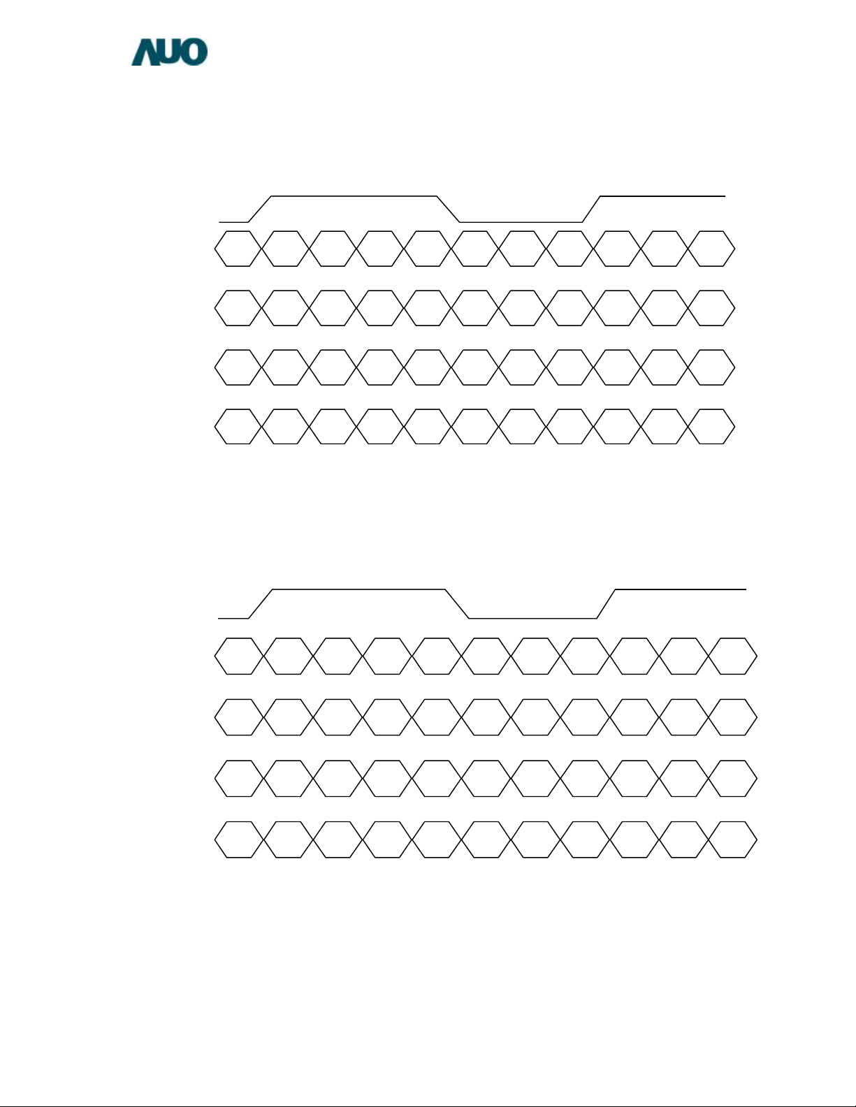
active area) shown as following:
©Copyright AU Optronics, Inc.
January, 2006 All Rights Reserved. T315XW01 VH - Specs. Ver 05 22/35
Page 23

T315XW01 VH (QD32HL05) 23of 32
Module
Serial Number Bar Code
Product Name
Module Quantity Per
Module Quantity
VH H00
13.Others
1) Lot No. Label:
Module Serial Number
Product Name
RATING: 5V 960mA(1400mA max)
INVERTER RATING: 24V 4.5A (5.0A Max)
01
MADE IN TAIWAN
2) Packing Label: 2 packing labels was attached on Carton shown as following.
:
Product Name
Bar Code
:
Lot No.: Date Code
Lot No. Bar Code
:
Carton
Bar Code
Carton No. Bar Code
©Copyright AU Optronics, Inc.
January, 2006 All Rights Reserved. T315XW01 VH - Specs. Ver 05 23/35
Digital 1-2 : Year ( 06 = 2006)
Digital 3 : Month (1,2,3,4,5,6,7,8,9,A,B,C)
Digital 4-5: Day.
Digital 6-10 : Carton Sequential Number.
Carton No.
Page 24

T315XW01 VH (QD32HL05) 24of 32
3) Pallet
By air transportation, there are 2-layer of cartons stacking on one pallet;
By ocean transportation, there are 3-layer of cartons stacking on one pallet.
For both air- and ocean- transportation, each layer has 6 cartons.
4) Maximum layer of carton 3-layer.
Notes:
1) Adjusting volume has been set optimally before shipment, so do not change any adjusted value. If adjusted
value is changed, the specification may not be satisfied.
2) Disassembling the module can cause permanent damage and should be strictly avoided.
3) Please be careful since image retention may occur when a fixed pattern is displayed for a long time.
4) If any problem occurs in relation to the description of this specification, it shall be resolved through
discussion with spirit of cooperation.
©Copyright AU Optronics, Inc.
January, 2006 All Rights Reserved. T315XW01 VH - Specs. Ver 05 24/35
Page 25

14. Drawing
Front View
T315XW01 VH (QD32HL05) 25of 32
©Copyright AU Optronics, Inc.
January, 2006 All Rights Reserved. T315XW01 VH - Specs. Ver 05 25/35
No Reproduction and Redistribution Allowed
Page 26

Back View
T315XW01 VH (QD32HL05) 26of 32
©Copyright AU Optronics, Inc.
January, 2006 All Rights Reserved. T315XW01 VH - Specs. Ver 05 26/35
No Reproduction and Redistribution Allowed
Page 27

T315XW01 VH (QD32HL05) 27of 32
15) Packing
15-1 Packing: By air transportation (1 of 2)
CORNER PAPER
COVER (TOP)
CARTON(3X2)
LDPE
透明伸縮膜
PALLET
Production
carton outline
carton weight
pallet outline
pallet weight
module/carton
module/stack
volume
Protecter paper
Corner paper
Cover
Cover Weight
total outline
total weights
V32(QD32HL) LCD MODULE
864(D)*380(W)*562(H)mm
35.5kg (include modules)
1200(D)*930(W)*130(H)mm
15 kg
4 pcs
24 pcs
m*m*m
1.42
1170*900 mm
50*50*750(8)mm(4x)
1200(L)x930(W)x100(H)mm,8t
0.8 kg
1200(D)*930(W)*1270(H)mm
228.8 kg
©Copyright AU Optronics, Inc.
January, 2006 All Rights Reserved. T315XW01 VH - Specs. Ver 05 27/35
No Reproduction and Redistribution Allowed
Page 28

T315XW01 VH (QD32HL05) 28of 32
Packing: By air transportation (2 of 2)
©Copyright AU Optronics, Inc.
January, 2006 All Rights Reserved. T315XW01 VH - Specs. Ver 05 28/35
No Reproduction and Redistribution Allowed
Page 29

T315XW01 VH (QD32HL05) 29of 32
15-2 Packing: By ocean transportation (1 of 2)
380
D
W
W
1
2
3
4
5
6
7
8
9
10
11
40" CONTAINER LOADING
(TOP VIEW)
D
12
864
13
14
15
16
17
18
COVER
W=1200(Pallet)
PATTERN B(1 LAYERS)
19
20
COVER
21
22
562+8*2=578
PATTERN A(2 LAYERS)
CONTAINER 40' & 20' CUBE LOADING PATTERN
100
562*2+8*2=1140 D=930(PALLET)
130
CONTAINER LOADING
CONTAINER SIZE
Q'ty
MODULES/CARTON
LOAD PATTERN
CARTONS/PALLET
PALLETS/CONTAINER
MODULES/PATTERN
TOTAL MODULES
20'
Production
carton outline
carton weight
pallet outline
pallet weight
module/carton
Pattern
1978
Protecter paper
Cover
Cover Weight
modules/pattern
Corner paper
Total volume
total outline
total weights
32"(QD32HL)LCD MODULE
864(D)*380(W)*562(H)mm
29.5kg(include modules)
1200(D)*930(W)*130(H)mm
15 kg
4 pcs
1170*900 mm
1200*930
0.8 kg
1200(D)*930(W)*1978(H)mm
251.1kg
40'
4
ABAB
6
22
582
3
22
264
846
AB
24 pcs
50*50*750(8)mm
m*m*m
2.21
10
240
6
20'
4
3
10
120
360
12 pcs
©Copyright AU Optronics, Inc.
January, 2006 All Rights Reserved. T315XW01 VH - Specs. Ver 05 29/35
No Reproduction and Redistribution Allowed
Page 30

T315XW01 VH (QD32HL05) 30of 32
Packing: By ocean transportation (2 of 2)
©Copyright AU Optronics, Inc.
January, 2006 All Rights Reserved. T315XW01 VH - Specs. Ver 05 30/35
No Reproduction and Redistribution Allowed
Page 31

T315XW01 VH (QD32HL05) 31of 32
There is no faital defect for the performance of the LCD module inspected by
module inspected by
There is no faital defect for the performance of the LCD module inspected by
There is no faital defect for the performance of the LCD module inspected by
There is no faital defect for the performance of the LCD module inspected by
here is no faital defect for the performance of the LCD module inspected by
There is no faital defect for the performance of the LCD module inspected by
There is no faital defect for the performance of the LCD module inspected by
16. Reliability test criteria
No.
Test item Conditions Judge Criteria
1 High temperature storage test
2 Low temperature storage test
3 High temperature
& High humidity operation
test
4 High temperature operation
test
5 Low temperature operation
test
6 Vibration test (non-
operating)
7 Shock test
(Non- operating)
8 ESD
Ta = 60℃, 500h
Ta = -25℃, 500h
Ta = 40℃, 95 %RH, 500h
Ta = 50℃, 500h
Ta = 0℃, 500h
Frequency: 10〜500Hz, 1.0G,
1Hr/each axis
Gravity: 100G
Pulse width: 2ms, half sine wave
Direction : ±X,±Y,±Z
Once for each
direction.
Contact-op: ±8kv, Contact-nop:
10kv,
Air-op: ±15kv, Air-nop: ±20kv,
(Contact area is limited on metal
bezel)
C: 150PF, R: 330Ω
the inspection method specified in Doc.NO. QD32HL05-01-IIS
There is no faital defect for the performance of the LCD
the inspection method specified in Doc.NO. QD32HL05-01-IIS
the inspection method specified in Doc.NO. QD32HL05-01-IIS
the inspection method specified in Doc.NO. QD32HL05-01-IIS
the inspection method specified in Doc.NO. QD32HL05-01-IIS
T
the inspection method specified in Doc.NO. QD32HL05-01-IIS
Active area must be inside of the bezel opening.
the inspection method specified in Doc.NO. QD32HL05-01-IIS
Active area must be inside of the bezel opening.
±
the inspection method specified in Doc.NO. QD32HL05-01-IIS
©Copyright AU Optronics, Inc.
January, 2006 All Rights Reserved. T315XW01 VH - Specs. Ver 05 31/35
No Reproduction and Redistribution Allowed
Page 32

T315XW01 VH (QD32HL05) 32of 32
There is no faital defect for the performance of the LCD module inspected by
9 Thermal cycle
10 High temperature operation
test 2
【Note1】Image sticking pattern shown as following:
Ta = -20, 1h ~ 60℃, 1h, 100 cycles
Ta =60℃, 200h
To check linear simi that occur
boundary between white and
black pattern.
【Note1】
3 x 3 - (V/7 x H/7) White
the inspection method specified in Doc.NO. QD32HL05-01-IIS
Cannot see any simi through the 10% ND filter at any gray scale at 60 degC.
Tentative criteria until the end of Feb:
Cannot see any simi through the 5% ND filter at 60 degC and through the
10% ND filter at 25 degC at any gray scale.
V/7
V
H/7
H/7
H
©Copyright AU Optronics, Inc.
January, 2006 All Rights Reserved. T315XW01 VH - Specs. Ver 05 32/35
No Reproduction and Redistribution Allowed
V/7
Black (Back ground)
 Loading...