

Page 1
TECHNICAL LITERATURE
TFT - LCD MODULE
No.
DATE Aug. 27. 2010
LD-K22575
MODEL No.
The technical literature is subject to change without notice.
So, please contact SHARP or its representative before designing
your product based on this literature.
LK315T3LA94
DEVELOPMENT DEPARTMENT. 1
LIQUID CRYSTAL DISPLAY DIVISION.1
LIQUID CRYSTAL DISPLAY GROUP
SHARP CORPORATION
Page 2
LK315T3LA94
RECORDS OF REVISION
SPEC No. DATE
No. PAGE
LD-K22575 Aug. 27. 2010 - - - 1st. Issue
REVISED
SUMMARY NOTE
Page 3

LD-K22575-1
Table of contents
1. Application.........................................................................................................................................2
2. Overview ............................................................................................................................................2
3. Mechanical specifications ..................................................................................................................2
4. Interface specifications ......................................................................................................................3
4.1. TFT panel driving............................................................................................................................. 3
4.2. LED driving..................................................................................................................................... 5
4.3. Interface block diagram..................................................................................................................... 6
4.4. Display position of data..................................................................................................................... 7
5. Back light lifetime .............................................................................................................................8
6. Absolute maximum ratings ...............................................................................................................8
7. Electrical characteristics ...................................................................................................................9
7.1. Control circuit .................................................................................................................................. 9
7.2. LED back light............................................................................................................................... 10
8. Timing characteristic of input and output signals.......................................................................... 11
8.1. Input data format .............................................................................................................................11
8.2. Timing characteristics of input signals .............................................................................................. 14
8.3. Control signals for 3D mode ............................................................................................................ 15
9. Input signal, basic display colors and gray scale of each color .......................................................18
10. Optical characteristics.....................................................................................................................19
10.1.
10.2. 3D mode .................................................................................................................................... 21
11. Reliability.........................................................................................................................................21
12. Packing form....................................................................................................................................21
13. Carton storage condition..................................................................................................................22
14. Precautions ......................................................................................................................................22
2D mode .................................................................................................................................... 19
Page 4
LD-K22575-2
1. Application
This technical literature applies to the color 31.5” TFT-LCD Module (LK315T3LA94).
* This technical literature is proprietary product of SHARP CORPORATION (“SHARP”) and includes materials
protected under copyright of SHARP. Do not reproduce or cause any third party to reproduce them in any form or by
any means, electronic or mechanical, for any purpose, in whole or in part, without the express written permission of
SHARP.
* In case of using the device for applications such as control and safety equipment for transportation (aircraft, trains,
automobiles, etc.), rescue and security equipment and various safety related equipment which require higher
reliability and safety, take into consideration that appropriate measures such as fail-safe functions and redundant
system design should be taken.
* Do not use the device for equipment that requires an extreme level of reliability, such as aerospace applications,
telecommunication equipment (trunk lines), nuclear power control equipment and medical or other equipment for
life support.
* SHARP assumes no responsibility for any damage resulting from the use of the device that does not comply with
the instructions and the precautions specified in this technical literature.
* Contact and consult with a SHARP sales representative for any questions about this device.
2. Overview
This module is a color active matrix LCD panel incorporating amorphous silicon TFT (Thin Film Transistor). It is
composed of a color TFT-LCD panel, driver ICs, Source-PWB, Control-PWB, optical sheets, LED-PWBs and
mechanical chassis.
Graphics and texts can be displayed on a 1366×RGB×768 dots panel with 16,777,216 colors by using LVDS (L
oltage Differential Signaling), I2C interface and +12V DC supply voltage, which are put into Control-PWB.
V
This module applies the Over Shoot driving (O/S driving) technology, signals are being applied to the Liquid
Crystal according to a pre-fixed process as image signals of the present frame when a difference is found between
image signals of the previous and current frame by comparing each other. The O/S driving technology makes the
Liquid Crystal response within 1 frame completely, motion blur reduce, so that clearer display performance can be
realized.
This module also can switch 2D and 3D mode to each other. In 2D mode, this can display images by converting
Single Frame Rate signals to Double Frame rate, while in 3D mode, by converting 3D input signals of Single Frame
Rate to pseudo-quarter Frame Rate. In both modes, FRC (Frame Rate Control) function operates.
ow
3. Mechanical specifications
Parameter Specifications Unit
Display size
Active area 697.69 (H) × 392.26 (V) mm
Pixel Format
Pixel pitch
Pixel configuration
Display mode
Outline Dimensions [Note1]
Mass
Surface treatment [Note2]
(Polarizer)
[Note1] Outline dimensions are shown in Fig.16 & 17.
[Note2] Without the protection film.
80.039 (Diagonal)
31.5 (Diagonal)
1366 (H) × 768 (V)
(1pixel = R + G + B dot)
0.51075(H) × 0.51075 (V)
R,G, B vertical stripe
Normally black
735.4(W) × 433.0(H) × (26.5)(D)
TBD
Low-Haze Anti Glare, Hard coating
Surface Hardness; 2H
cm
inch
pixel
mm
mm
kg
Page 5
Interface specifications
V
4.
LD-K22575-3
4.1.
TFT panel driving
CN1 (Interface signals and +12V DC power supply; shown in Fig.1)
Used connector: GT103-30S-H23-D-E2500 (LSMtron) or IS100-L30B-C23 (UJU)
Mated connector: FI-X30H/FI-X30HL, FI-X30C/FI-X30C2L
or FI-X30M (Japan Aviation Electronics Ind. , Ltd.)
Mated LVDS transmitter: THC63LVDM83R (THine) or equivalent device
Pin No. Symbol Function Type Remark
1 VCC +12V Power Supply I
2 VCC +12V Power Supply I
3 VCC +12V Power Supply I
4 VCC +12V Power Supply I
5 GND
6 GND
7 SDA
8 SCL
9 Reserved
10 Reserved
11 GND
12 RIN013 RIN0+
14 GND
15 RIN116 RIN1+
17 GND
18 RIN219 RIN2+
20 GND
21 CLKIN22 CLKIN+
23 GND
24 RIN325 RIN3+
26 GND
27 FST
28 LST
29
LRI
Ground
Ground
I2C data
I2C clock
Not available
Not available
Ground
Negative (-) LVDS differential data input
Positive (+) LVDS differential data input
Ground
Negative (-) LVDS differential data input
Positive (+) LVDS differential data input
Ground
Negative (-) LVDS differential data input
Positive (+) LVDS differential data input
Ground
Clock Signal(-)
Clock Signal(+)
Ground
Negative (-) LVDS differential data input
Positive (+) LVDS differential data input
Ground
Frame start signal
Line start signal
Discriminating signal either left or right eye data
I
I
I/O [Note1]
I/O [Note1]
-
-
I
I [Note 6]
I [Note 6]
I
I [Note 6]
I [Note 6]
I
I [Note 6]
I [Note 6]
I
I [Note 6]
I [Note 6]
I
I [Note 6]
I [Note 6]
I
O [Note 2, 5]
O [Note 2, 5]
I [Note 3, 5]
(for 3D frame alternative mode only)
30
GLS
Glass shutter control signal
O [Note 4, 5]
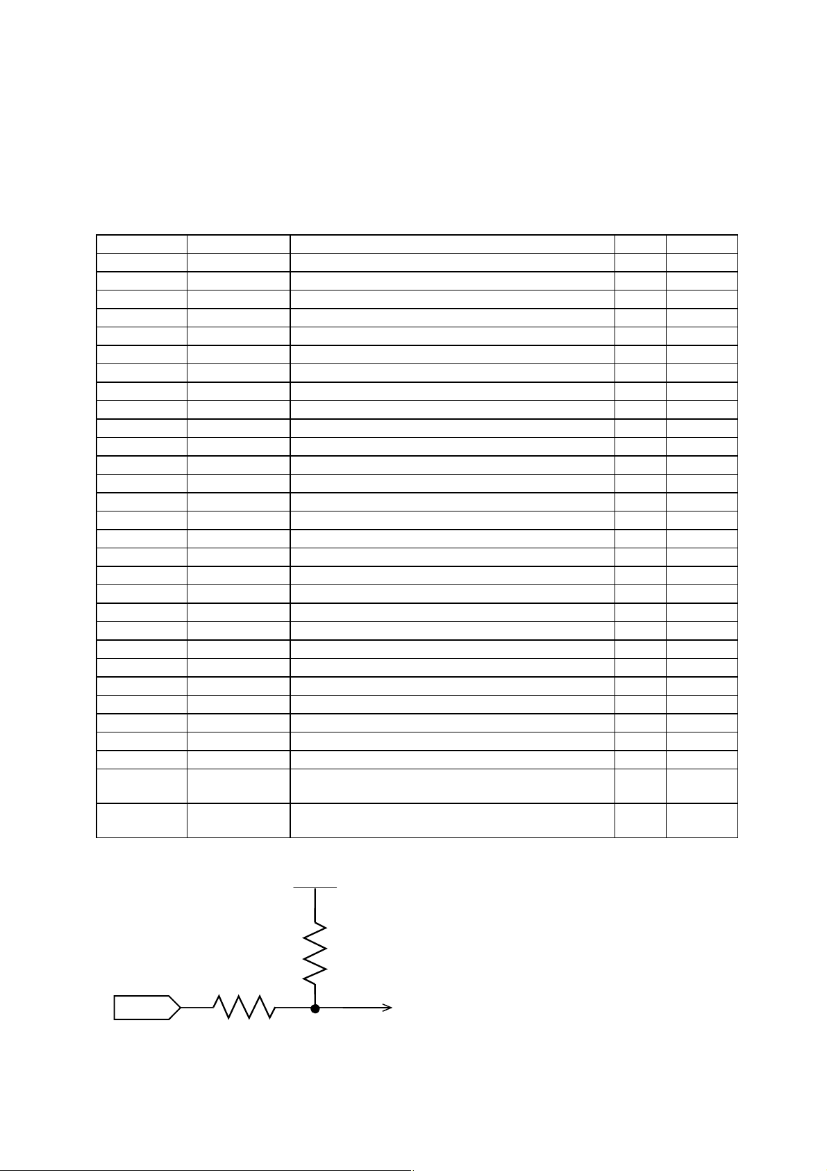
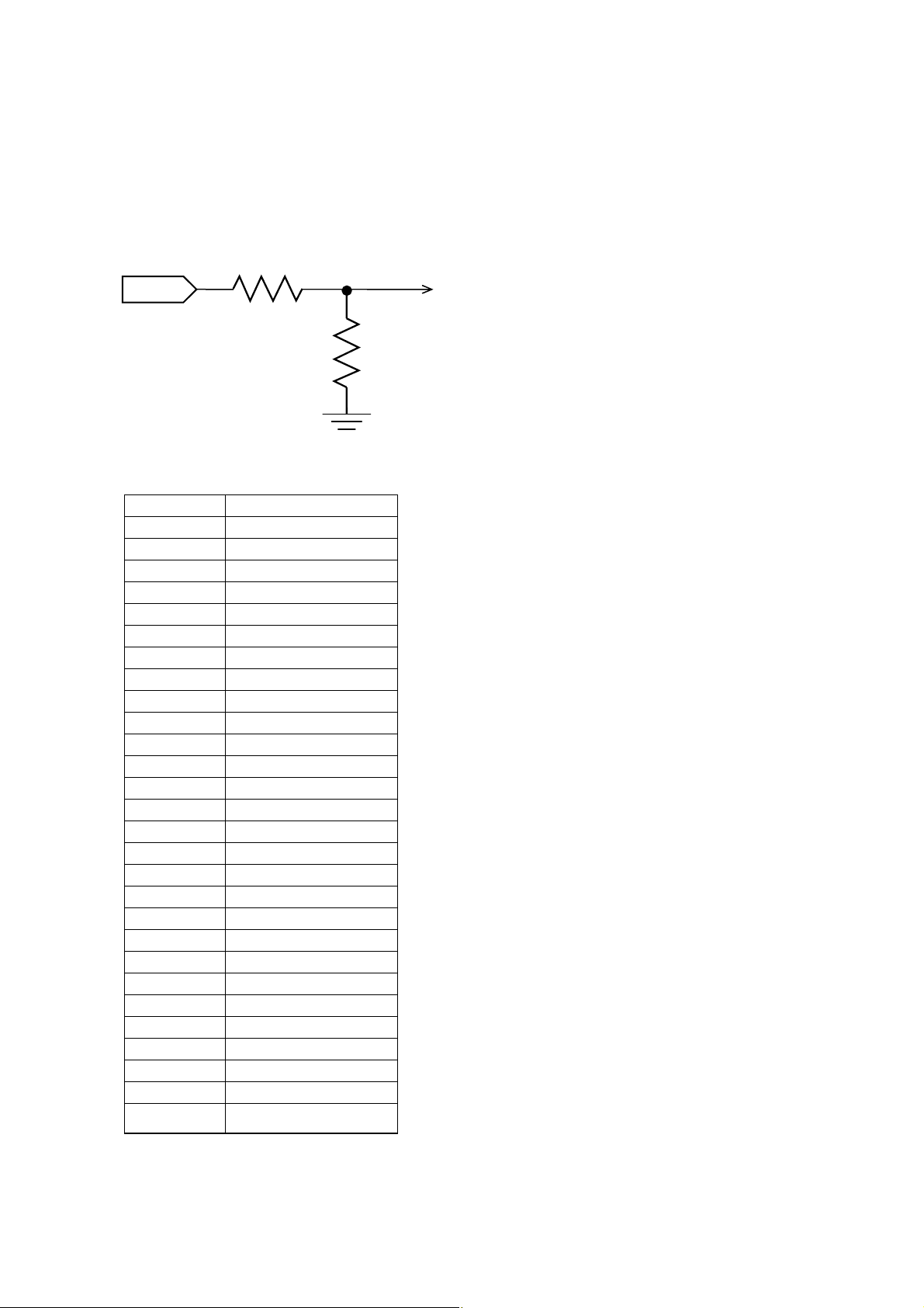
[Note 1] These signals are I2C interface, used to control 2D/3D data. The equivalent circuit figure of these terminals
as below:
CC
0 [Ω]
Ter mi na l
2K [Ω]
[Note 2]
These signals are used for LED-ON/OFF scanning. Timing characteristic of them is explained in section 8.2.
Page 6
LD-K22575-4
[Note 3]
This signal is used to distinguish Left eye data from Right eye data for 3D frame alternative mode only. Timing
characteristic of this signal is explained in section 8.3.
[Note 4]
If you connect this signal to your emitter device and glass, you can synchronize glass shutter timing with 3D data
and see 3D contents. Timing characteristic of this signal is explained in section 8.3.
[Note 5] The equivalent circuit figure of these terminals is as below:
0 [Ω]
Ter mi na l
2K [Ω]
GND
[Note 6] The LVDS data order corresponds to VESA format only in this module. Please input LVDS data as follows:
Transmitter
TA0
TA1
TA2
TA3
TA4
TA5
TA6
TB0
TB1
TB2
TB3
TB4
TB5
TB6
TC0
TC1
TC2
TC3
TC4
TC5
TC6
TD0
TD1
TD2
TD3
TD4
TD5
TD6
Data
R0(LSB)
R1
R2
R3
R4
R5
G0(LSB)
G1
G2
G3
G4
G5
B0(LSB)
B1
B2
B3
B4
B5
NA
NA
DE(*)
R6
R7(MSB)
G6
G7(MSB)
B6
B7(MSB)
NA
NA: Not Available (Fixed Low)
(*) Since the display position is prescribed by the rise of DE (Display Enable) signal, please do not fix DE signal
during operation at "High."
Page 7
LD-K22575-5
1 cycle
CLKIN+
CLKIN-
RIN0+
G0 R5 R4 R3 R2 R1 R0 R0 R1 G0
RIN0-
RIN1+
B1 B0 G5 G4 G3 G2 G1 G1 G2 B1
RIN1-
RIN2+
DE
NA NA
B5 B4 B3 B2 B2 B3
DE
RIN2-
RIN3+
B7 B6 G7 G6 R7 R6 R6 R7 NA NA
RIN3-
NA: Not Available (Fixed Low)
DE: Display Enable
Fig. 1 LVDS input data format
4.2.
You should adjust LED current to 0.525A. (I
LED driving
=0.525A , V
LED
=about 92V).
LED
CN101 (+525mA DC power supply)
Using connector: 51103-0400 (Molex)
TBD
Mating connector: XAP-04V-1 (JST)
Pin No. Symbol Function Default(OPEN) Input Impedance Remark
1 I
2 I
3
Reserved
4 Reserved - -
Input LED current
+LED
Input LED current
+LED
Page 8
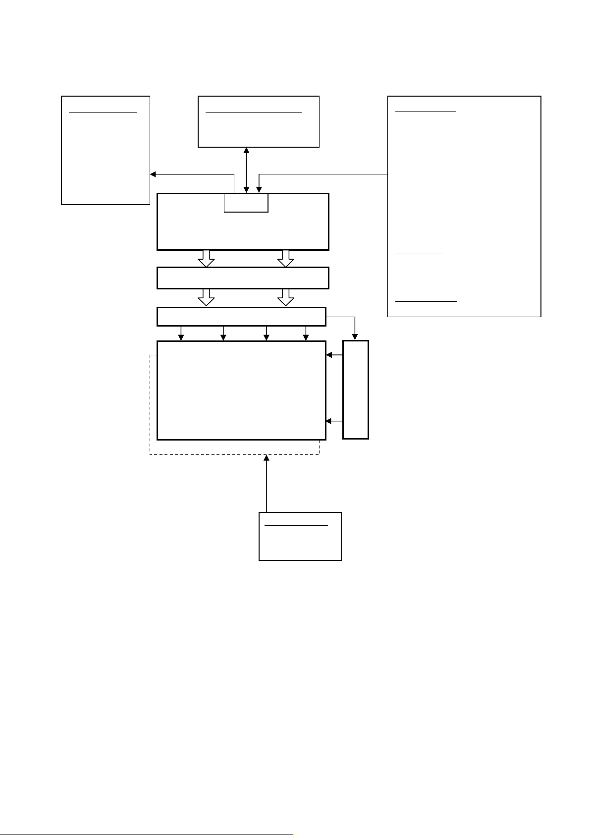
4.3.
Interface block diagram
Output signals
FST
LST
(for control LED)
GLS
(to emitter, glass)
LED-BACK LIGHT
LD-K22575-6
Control signals (I2C)
SDA
SCL
CN1
Control PWB
Source PWB
Source driver
Input signals
CLKIN+
CLKINRIN0+
RIN0RIN1+
RIN1RIN2+
RIN2RIN3+
RIN3-
3D signals
LRI
(frame alternative mode only)
Power supply
+12V DC
LCD panel
1366×3(RGB)×768
Gate driver
Power Supply
(CN101)
=0.525A
I
LED
Fig. 2 Interface block diagram
Page 9

4.4.
Display position of data
B1 G1 R1 B2 G2 R2
(1、1) (1,2 )
1・1 1・2 1・3
2・1 2・2
3・1
768 ・1
Fig. 3 Display position of data (V, H)
LD-K22575-7
1・13 6 6
B
G R
768・1366
Page 10

LD-K22575-8
Back light lifetime
5.
The back light system is direct type with LED packages. The characteristics of the back light are shown as below:
Item Symbol Min. Typ. Max. Unit Remarks
Life time TLED TBD TBD - Hour [Note]
[Note] The value of life time is per one LED.
LED life time is defined as the time when brightness becomes 50% of the original value in the continuous
operation under the condition of TC(Temperature of LED terminal)=85℃.
Absolute maximum ratings
6.
Parameter Symbol Condition Ratings Unit Remark
Input voltage
(for Control PWB)
+12V supply voltage
(for Control PWB)
Input voltage
(for LED)
Input current
(for LED)
I Ta=25°C -0.3 ~+ 3.6 V [Note 1]
V
Ta=25°C -0.3 ~+18 V
V
CC
Ta=25°C TBD V
V
LED
Ta=25°C TBD A
I
LED
Storage temperature Tstg - -25 ~ +60 °C
Operation temperature
(Ambient)
Topa - 0 ~ +50 °C
[Note 1] SDA, SCL, GSP, GCK, LRI, LRO
[Note 2] Humidity 95%RH Max.(Ta ≤ 40°C)
Maximum wet-bulb temperature is 39°C or less (Ta > 40°C). No condensation.
[Note 2]
Page 11

Electrical characteristics
C
0
4
(
)
7.
LD-K22575-9
7.1.
Control circuit
Ta=25°C
Parameter Symbol Min. Typ. Max. Uniit Remark
Supply voltage VCC (+11.4) +12.0 (+12.6) V [Note 1]
ICC - TBD mA [Note 2]
I
T
V
RUSH
RUSH
RP
-
TBD
mA
- TBD - ms [Note 6]
- - TBD mV
P-P
[Note 6]
Vcc = +12.0V
*V
CM = +1.2V
[Note 4]
- 100 - Ω LVDS input
T
[Note 3]
I = 0V
- - TBD µA
I
IL
I
- - TBD µA
IH
2.6 3.3 V
OH
V
[Note 3]
I =3.3V
V
[Note 3]
[Note 5]
+12V DC power
Differential
signal
Input voltage
Output voltage
Current
consumption
Permissible input
ripple voltage
Threshold high VTH - - TBD mV
Threshold low VTL TBD - - mV
Terminal resistor R
Low voltage VIL 0 - 0.7 V
High voltage VIH 2.6 - 3.3 V
Leak current
(Low)
Leak current
(High)
Low voltage VOL 0 - 0.7 V
High voltage V
[Note] *VCM: Common mode voltage of LVDS driver.
[Note 1]
Input voltage sequences Dip conditions for supply voltage
TBD < t1 ≤ TBD a) TBD ≤ V
< TBD V
CC
TBD < t2-1 td ≤ TBD
TBD < t2-2 b) VCC < TBD
0 < t3 ≤ TBD Dip conditions for supply voltage is
t4 ≥ TBD based on input voltage sequence.
t5 ≥ TBD
.9VCC
0.1 V
CC
V
C
t1
Data1
Data2
LED B/L: VLED
t2-1
t2-2
0.9 VCC
0.1VCC
t3
t5
ON
0.1 V
t4
OFFOFF
CC
V
(
T
7
B
.
D
2
)
td
Vcc
V
T
B
5
D
.
V
※ Data1: CLKIN±,RIN0±,RIN1±, RIN2±, RIN3±
※ Data2: SDA, SCL, LRI
※ About the relation between data input and back light lighting, we recommend the above-mentioned input
sequence.
If the back light is switched on before a panel operation begins or after a panel operation stops, the screen may
not be displayed properly. But this phenomenon is not caused by change of an incoming signal, and does not
give damage to a liquid crystal display.
Page 12

[Note 2]Typical current situation: 256 gray-bar pattern (V
= +12.0V)
CC
The explanation of RGB gray scale is seen in section 8.
RGB
GS0
RGB
GS1
RGB
GS2
....
RGB
GS254
RGB
GS255
VCC = +12.0V
CK = 82.0MHz
Th = 20.68μs
[Note 3] SDA, SCL, LRI
[Note 4] CLKIN+/CLKIN-, RIN0+/RIN0-, RIN1+/RIN1-, RIN2+/RIN2-, RIN3+/RIN3-
[Note 5] FST, LST, GLS
[Note 6] The rush current corrugation at the time of power on: TBD
7.2.
LED back light
Parameter Symbol Min. Typ. Max. Unit Remark
LD-K22575-10
Ta=25℃
LED Current ILED (0.525) A
Tc≦85℃ [Note1]
LED Voltage VLED (92) V [Note2]
[Note1] LED current (I
) is the value of total packages. It must be controlled to keep Tc lower than 85℃.
LED
[Note2] Ta = 25℃, Measurement after 1hour has passed since power supply was turned on.
Page 13

Timing characteristic of input and output signals
8.
LD-K22575-11
8.1.
You need to send I2C command in order to start up. At first you send target device command, next input data format
command to each register. Slave address of target device should be set to “0x5A”. Register command table is as
follows:
[Note] We recommend SOC device of input signals are MSD3819JX, MSD3819SV (for digital TV) and MST6300RS,
MST6100VS (for analog TV).
Input data format diagrams are shown as follows. Please refer to section 8.2 about the range of TH, TV, THd and
TVd.
Input data format
*Slave address (7bit) : 0x5A
Register address Description Definition
0x 0000 I2C status 0 : Busy
1 : OK
0x 0010 Target device 00 (fixed)
0x 0030 Input data format 00: 2D mode
81: Side by Side
82: Top and Bottom
83: Frame Alternative
84: Frame Packing
THd(Horizontal Active)
TV
TVd
Active Area
(Vertical Active)
TH
Fig. 4 2D mode
Page 14

LD-K22575-12
THd(Horizontal Active)
TV
TVd
L R
(Vertical Active)
THd/2THd/2
TH
Fig. 5 3D-Side by Side mode
THd(Horizontal Active)
L
TV
TVd/2
TVd/2
R
(Vertical Active)
TH
Fig. 6 3D-Top and Bottom mode
Page 15

THd(Horizontal Active)
Tentative
LD-K22575-13
TV
TVd
L
(Vertical Active)
TV
R
TH
Fig. 7 3D-Frame Alternative mode (TBD)
THd(Horizontal Active)
TVd
(Vertical Active)
TV
TVd
L
(Vertical Active)
R
TH
Fig. 8 3D-Frame Packing mode (TBD)
TVd/2
Page 16

8.2.
Timing characteristics of input signals
Timing diagrams of input signal are shown in Fig.9.
[2D mode / 3D mode Side by Side, Top and Bottom]
Parameter Symbol Min. Typ. Max. Unit
Clock Frequency 1/Tc TBD 82 TBD MHz
LD-K22575-14
Horizontal period TH
Data enable
signal
[3D mode / Frame Alternative]
Clock Frequency 1/Tc TBD TBD TBD MHz
Data enable
signal
[3D mode / Frame Packing]
Horizontal period (High) THd - 1366 - clock
Vertical period TV TBD 806 TBD line
Vertical period (High) TVd - 768 - line
Parameter Symbol Min. Typ. Max. Unit
Horizontal period TH
Horizontal period (High) THd - TBD - clock
Vertical period TV TBD TBD TBD line
Vertical period (High) TVd - TBD - line
TBD 1696 TBD clock
TBD 20.68 - µs
TBD TBD TBD clock
TBD TBD - µs
Parameter Symbol Min. Typ. Max. Unit
Clock Frequency 1/Tc TBD TBD TBD MHz
Horizontal period TH
Data enable
signal
[Note] *When a vertical period is very long, a flicker may occur.
Horizontal period (High) THd - TBD - clock
Vertical period TV TBD TBD TBD line
Vertical period (High) TVd - TBD - line
*Please turn off the module after it shows the black screen.
*Please make sure that a length of vertical period should be an integral multiple of horizontal period,
otherwise the screen may not display properly.
*Please be careful not to fall below the minimum horizontal period, otherwise the display may be dark.
TBD TBD TBD clock
TBD TBD - µs
Page 17

LD-K22575-15
TH
THd
DE
DATA
(R, G, B)
1366
1 2
1366
Tc
1 2 N
N-1
DE
TV
TVd
Fig. 9 Timing diagram of input signals
8.3.
[Input signal] LRI
Control signals for 3D mode
LRI indicates the status of either left or right eye data for 3D frame alternative mode only. When LRI is ‘High’,
input data is recognized as Right eye data. When LRI is ‘Low’, input data is recognized as Left eye data.
If you use 3D frame alternative mode, you should input LRI synchronized with data as below. In other modes, LRI
is not used. (Don’t care)
T
LRIL
LRI
DE
(LVDS input)
T
LRIH
Right data Left data Right data
t
t
LR1
LR2
Fig. 10 LRI timing diagram
Parameter Symbol Min. Typ. Max. unit
High time of LRI
Low time of LRI
LRI High to DE rise edge t
DE High to LRI fall edge t
T
LRIH
T
LRIL
TBD TBD TBD us
LR1
TBD TBD TBD us
LR2
- T
- T
-
V
-
V
Page 18

LD-K22575-16
[Output signal] FST, LST, GLS
FST is a frame start pulse and output by the period of T
/2. LST is a line start pulse and output by the period of TH.
V
Since they can be used for control LED-ON/OFF duty, you may design any device able to control LED. These signals
are fixed at ‘Low’ in 2D mode.
GLS is a rectangular signal to control glass shutter timing, reversed by period of TV/2 and synchronized with FST.
You connect this signal to your emitter device in order to control opening and closing glass shutter. This signal is
fixed at ‘Low’ in 2D mode.
The timing diagram between these signals and data is shown in Fig. 12.
T
GLS
t
FSG1
T
FST
GLS
t
FSG2
FST
t
T
LSTW
FSL1
t
FSL2
LST
T
LST
Fig. 11 Timing diagram of GLS, FST, and LST
Parameter Symbol Min. Typ. Max. unit
Reverse period of GLS T
- TV/2 -
GLS
Period of FST T
Width of LST T
- TV/2 -
FST
TBD TBD TBD us
LSTW
Period of LST T
Time from FST rise to GLS rise
- TH -
LST
t
TBD TBD TBD us
FSG1
edge
Time from FST rise to GLS fall
t
TBD TBD TBD us
FSG2
edge
Time from FST rise to GLS rise
tFSL1 TBD TBD TBD us
edge
Time from LST rise to GLS fall
tFSL2 TBD TBD TBD us
edge
Page 19

LD-K22575-17
T
V
Panel Output
GLS
[Note 1]
Back Light
[Note 1]
FST
LST
R
data
Glass L open Glass R open
OFF
R
data
Glass R open Glass L open
ON
L
data
OFF
L
data
ON
TV /2
R
data
OFF
TV /2
R
data
ON
T
H
Fig. 12 The timing diagram between LED control signals and data (3D mode)
[Note 1]
The way of glass shutter opening is depended on each 3D glass. Above diagram is an example of the condition;
・Left glass open and right glass close when GLS is ‘H’
・Left glass close and right glass open when GLS is ‘L’.
When you use 3D glass different from above mentioned type, you should reverse the order of LED-ON/OFF.
Page 20

Input signal, basic display colors and gray scale of each color
9.
LD-K22575-18
Colors &
Gray scale
Black
Blue
Green
Cyan
Red
Basic Color
Magenta
Yellow
White
Black GS0 0 0 0 0 0 0 0 0 0 0 0 0 0 0 0 0 0 0 0 0 0 0 0 0
Darker GS2 0 1 0 0 0 0 0 0 0 0 0 0 0 0 0 0 0 0 0 0 0 0 0 0
Brighter GS253 1 0 1 1 1 1 1 1 0 0 0 0 0 0 0 0 0 0 0 0 0 0 0 0
Gray Scale of Red
Red GS255 1 1 1 1 1 1 1 1 0 0 0 0 0 0 0 0 0 0 0 0 0 0 0 0
Gray
R0 R1 R2 R3 R4 R5 R6 R7 G0 G1 G2 G3 G4 G5 G6 G7 B0 B1 B2 B3 B4 B5 B6 B7
Scale
0 0 0 0 0 0 0 0 0 0 0 0 0 0 0 0 0 0 0 0 0 0 0 0
-
0 0 0 0 0 0 0 0 0 0 0 0 0 0 0 0 1 1 1 1 1 1 1 1
-
0 0 0 0 0 0 0 0 1 1 1 1 1 1 1 1 0 0 0 0 0 0 0 0
-
0 0 0 0 0 0 0 0 1 1 1 1 1 1 1 1 1 1 1 1 1 1 1 1
-
1 1 1 1 1 1 1 1 0 0 0 0 0 0 0 0 0 0 0 0 0 0 0 0
-
1 1 1 1 1 1 1 1 0 0 0 0 0 0 0 0 1 1 1 1 1 1 1 1
-
1 1 1 1 1 1 1 1 1 1 1 1 1 1 1 1 0 0 0 0 0 0 0 0
-
1 1 1 1 1 1 1 1 1 1 1 1 1 1 1 1 1 1 1 1 1 1 1 1
-
GS1 1 0 0 0 0 0 0 0 0 0 0 0 0 0 0 0 0 0 0 0 0 0 0 0
×
×
Ø
GS254 0 1 1 1 1 1 1 1 0 0 0 0 0 0 0 0 0 0 0 0 0 0 0 0
Ø
È
È
È
È
Data signal
È
È
È
È
Black GS0 0 0 0 0 0 0 0 0 0 0 0 0 0 0 0 0 0 0 0 0 0 0 0 0
GS1 0 0 0 0 0 0 0 0 1 0 0 0 0 0 0 0 0 0 0 0 0 0 0 0
×
Darker GS2 0 0 0 0 0 0 0 0 0 1 0 0 0 0 0 0 0 0 0 0 0 0 0 0
×
Ø
Brighter GS253 0 0 0 0 0 0 0 0 1 0 1 1 1 1 1 1 0 0 0 0 0 0 0 0
Gray Scale of Green
GS254 0 0 0 0 0 0 0 0 0 1 1 1 1 1 1 1 0 0 0 0 0 0 0 0
Ø
Green GS255 0 0 0 0 0 0 0 0 1 1 1 1 1 1 1 1 0 0 0 0 0 0 0 0
Black GS0 0 0 0 0 0 0 0 0 0 0 0 0 0 0 0 0 0 0 0 0 0 0 0 0
GS1 0 0 0 0 0 0 0 0 0 0 0 0 0 0 0 0 1 0 0 0 0 0 0 0
×
Darker GS2 0 0 0 0 0 0 0 0 0 0 0 0 0 0 0 0 0 1 0 0 0 0 0 0
×
Ø
Brighter GS253 0 0 0 0 0 0 0 0 0 0 0 0 0 0 0 0 1 0 1 1 1 1 1 1
È
È
È
È
È
È
È
È
È
È
È
È
È
È
È
È
Gray Scale of Blue
GS254 0 0 0 0 0 0 0 0 0 0 0 0 0 0 0 0 0 1 1 1 1 1 1 1
Ø
Blue GS255 0 0 0 0 0 0 0 0 0 0 0 0 0 0 0 0 1 1 1 1 1 1 1 1
0: Low level voltage 1: High level voltage
Each basic color can be displayed in 256 gray scales from 8 bit data signals. According to the combination of total
24 bit data signals, the 16,777,216 colors can be displayed on the screen.
Page 21

Optical characteristics
10.
10.1. 2D mode
Parameter Symbol Condition Min. Typ. Max. Unit Remark
Viewing angle
range
Horizontal
Vertical
Contrast ratio CRn (TBD) (5000) - - [Note2,4]
θ21
θ22
θ11
θ12
CR ≥ 10
Ta = 25°C, Vcc = +12V, V
= (92V), ILED = 0.525A
LED
70 88 - Deg.
70 88 - Deg.
LD-K22575-19
[Note1,4]
Response time
Chromaticity of white
Chromaticity of red
Chromaticity of green
Chromaticity of blue
τ
DRV
x Typ.-0.03
y Typ.-0.03
θ
x Typ.-0.03
=0 deg.
y Typ.-0.03
x Typ.-0.03
y Typ.-0.03
x Typ.-0.03
y
Luminance of white YL (TBD) (450) cd/m2
- (4) - ms [Note3,4,5]
Typ.-0.03
TBD
TBD
TBD Typ.+0.03
TBD Typ.+0.03
TBD Typ.+0.03
TBD Typ.+0.03
TBD Typ.+0.03
TBD Typ.+0.03
Typ.+0.03 Typ.+0.03 -
-
-
-
-
-
-
[Note 4]
[Note 4]
Luminance uniformity δW - - TBD - [Note 6]
*The measurement shall be executed 60 minutes after turning on.
*These characteristics are for 2D mode only.
[Note] The optical characteristics are measured using the following equipment.
Detector (EZ-CONTRAST, Photo diode)
Detector (equivalent to SR-3A-UL1)
400mm
Field=1°
Center of the screen (θ = 0°)
Center of the screen (θ = 0°)
TFT-LCD module
TFT-LCD module
Fig. 13 Measurement of viewing angle range Fig. 14 Measurement of Contrast,
and response time. Luminance, and Chromaticity.
(Viewing angle range: EZ-CONTRAST
Response time: Photo diode)
Page 22

[Note 1] Definitions of viewing angle range:
LD-K22575-20
Normal
θ11
θ21
θ12
θ22
6 o’clock direction
[Note 2] Definition of contrast ratio:
The contrast ratio is defined as the following.
Luminance (brightness) with all pixels white
Contrast ratio
=
Luminance (brightness) with all pixels black
[Note 3] Definition of response time
The response time (τ
) is defined as the following equation and shall be measured by switching the input
DRV
signal from “any level of gray (0%, 25%, 50%, 75% and 100%)” to “any level of gray (0%, 25%, 50%, 75% and
100%)”.
0%
0%
25%
50%
75%
100%
td: 25%-0%
td: 50%-0% td: 50%-25%
td: 75%-0% td: 75%-25% td: 75%-50%
td: 100%-0% td: 100%-25% td: 100%-50% td: 100%-75%
25% 50% 75%
tr: 0%-25%
tr: 0%-50% tr: 0%-75% tr: 0%-100%
tr: 25%-50% tr: 25%-75% tr: 25%-100%
τ
= Σ(t*:x-y)/20
DRV
t*:x-y...response time from level of gray(x) to gray(y)
Bright Bright Dark
100%
90%
Photodetector
10%
Output
0%
τd τr
Fig. 15 Response time of fall (τ
Time
) and rise (τr)
d
[Note 4] This shall be measured at center of the screen.
[Note 5] This value is valid when O/S driving is used at typical input timing.
100%
tr: 50%-75% tr: 50%-100%
tr: 75%-100%
Page 23

[Note 6] Definition of white uniformity;
White uniformity is defined as the following with five measurements. (A~E)
Maximum luminance of five points (brightness)
W=
δ
Minimum luminance of five points (brightness)
10.2. 3D mode
TBD
683 1024
342
A
C
B
LD-K22575-21
pixel
D
E
192
384
576
pixel
Reliability
11.
Reliability test item:
No. Test item Condition
1
2
3
4
5
High temperature storage test
Low temperature storage test
High temperature and high humidity
operation test
High temperature operation test
Low temperature operation test
Ta=60°C 240h
Ta=-25°C 240h
Ta=40°C ; 95%RH 240h
(No condensation)
Ta=50°C 240h
Ta=0°C 240h
Packing form
12.
a) Piling number of cartons: TBD / 1pallette.
b) Packing quantity in one carton: TBD pcs
c) Carton size: TBD(W) × TBD(D) × TBD(H)
d) Total mass of one carton filled with full modules: TBD(Max)
Page 24

LD-K22575-22
Carton storage condition
13.
a) Temperature: 0°C to 40°C
b) Humidity: 95%RH or less
Reference condition: 20°C to 35°C, 85%RH or less (summer)
: 5°C to 15°C, 85%RH or less (winter)
The total storage time (40°C, 95%RH): 240H or less
c) Sunlight:
Be sure to shelter a product from the direct sunlight.
d) Atmosphere:
Do not store in a place where exists the risk of corrosive gas (such as acid and alkali) or volatile solvents.
e) Prevent condensation:
Be sure to put cartons on a palette or base, don’t put it on the floor, and store them keeping off the wall.
Please take care of ventilation in storehouse and around cartons, and control temperature not to change abruptly
beyond the natural environment.
f) Storage life: 1 year
Precautions
14.
a) Be sure to turn off the power supply when inserting or disconnecting the cable.
b) Be sure to design the cabinet so that the module can be installed without any extra stress such as warp or
twist.
c) Since the front polarizer is easily damaged, pay attention not to scratch it.
d) Since long contact with water may cause discoloration or spots, wipe off water drop immediately.
e) When the panel surface is soiled, wipe it with absorbent cotton or other soft cloth.
f) Since the panel is made of glass, it may break or crack if dropped or bumped on hard surface. Handle with
care.
g) Since CMOS LSI is used in this module, take care of static electricity and take the human earth into
consideration when handling.
h) The module has some printed circuit boards (PCBs) on the back side, take care to keep them form any stress
or pressure when handling or installing the module; otherwise some of electronic parts on the PCBs may be
damaged.
i) Observe all other precautionary requirements in handling components.
j) When some pressure is added onto the module from rear side constantly, it causes display non-uniformity
issue, functional defect, etc. So, please avoid such design.
k) When giving a touch to the panel at power on supply, it may cause some kinds of degradation. In that case,
once turn off the power supply, and turn on after several seconds again, and that is disappear.
l) When handling LCD modules and assembling them into cabinets, please be noted that long-term storage in
the environment of oxidization or deoxidization gas and the use of such materials as reagent, solvent,
adhesive, resin, etc. which generate these gasses, may cause corrosion and discoloration of the LCD
modules.
m) This LCD module is designed to prevent dust from entering into it. However, there would be a possibility to
have a bad effect on display performance in case of having dust inside of LCD module. Therefore,
please ensure to design your TV set to keep dust away around LCD module.
Page 25

Page 26

 Loading...