

Page 1
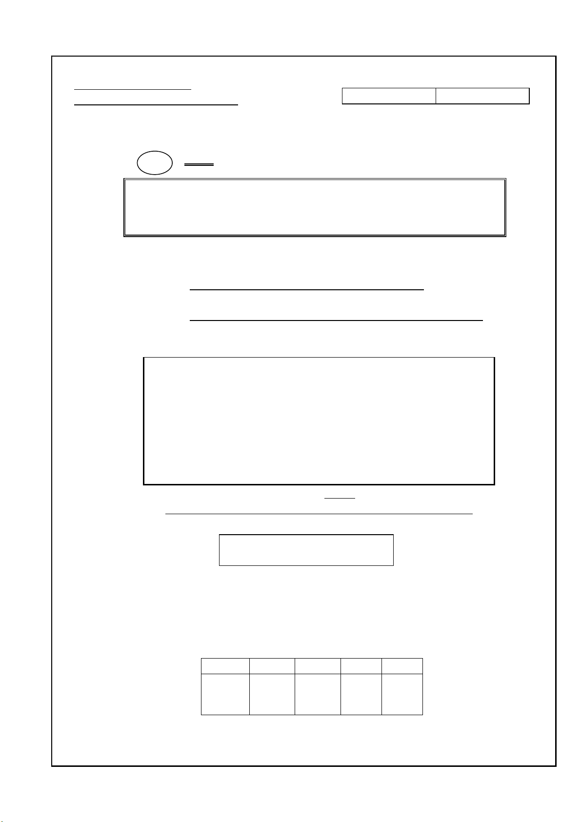
AVシステム事業本部
液晶DS第四事業部 技術部殿
LD-K23Z03 -1
納入仕様書番号
作成日 2012年 1月 6日
改訂日 年 月 日
LD-K23Z03
《新規・変更》
品名 TFT-LCDモジュール
形名 LK315T3HB00X/T/A
【受領印欄】
納 入 仕 様 書
※この仕様書は、付属書等を含めて全21頁で構成されております。
当仕様書について異議があれば発注時点までにお申し出ください。
RoHS規制対応部品
シャープ株式会社
大型液晶事業本部
液晶事業部 第二開発部
所属長 参事 副参事 係長 担当
三重県亀山市白木町幸川464番地
Page 2
MODEL No. : LK315T3HB00X/T/A
SPEC No. : LD-K23Z03
DATE
2012.1.6
NO.
LD-K23Z03
RECORDS OF REVISION
REVISED
No.
-
PAGE SUMMARY NOTE
- -
LD-K23Z03 -2
1st Issue
Page 3
LD-K23Z03 -3
1. Application
This specification applies to the color 31.5” Wide XGA TFT Open-Cell LK315T3HB00X/T/A.
* These specification sheets are proprietary products of SHARP CORPORATION (“SHARP”) and include materials
protected under copyright of SHARP. Do not reproduce or cause any third party to reproduce them in any form or by
any means, electronic or mechanical, for any purpose, in whole or in part, without the express written permission of
SHARP.
* In case of using the device for applications such as control and safety equipment for transportation (aircraft, trains,
automobiles, etc.), rescue and security equipment and various safety related equipment which require higher
reliability and safety, take into consideration that appropriate measures such as fail-safe functions and redundant
system design should be taken.
* Do not use the device for equipment that requires an extreme level of reliability, such as aerospace applications,
telecommunication equipment (trunk lines), nuclear power control equipment and medical or other equipment for
life support.
* SHARP assumes no responsibility for any damage resulting from the use of the device that does not comply with
the instructions and the precautions specified in these specification sheets.
* Contact and consult with a SHARP sales representative for any questions about this device.
2. Overview
This Open-Cell is a color active matrix LCD module incorporating amorphous silicon TFT (T
It is composed of a color TFT-LCD panel, driver ICs, control circuit, power supply circuit, inverter circuit and back
light system etc. Graphics and texts can be displayed on a 1366×RGB×768 dots panel with 16,777,216 colors by
using LVDS (L
This module also includes the LED-PWB module to drive the LED.
And in order to improve the response time of LCD, this module applies the Over Shoot driving (O/S driving)
technology for the control circuit .In the O/S driving technology, signals are being applied to the Liquid Crystal
according to a pre-fixed process as an image signal of the present frame when a difference is found between image
signal of the previous frame and that of the current frame after comparing them.
By using the captioned process, the image signals of this Open-Cell are being set so that image response can be
completed within one frame, as a result, image blur can be improved and clear image performance can be realized.
3. Mechanical Specifications
Active area 697.69 (H) × 392.26 (V) mm
Pixel Format
Pixel pitch 0.51075(H) × 0.51075 (V) mm
Pixel configuration R,G, B vertical stripe
Display mode Normally black
Unit Outline Dimensions (*1) 709.3(W) × 451.2(H) ×4.8max(D) mm
Mass 1.2 kg
Surface treatment
(*1) Outline dimensions are shown in Fig.1
ow Voltage Differential Signaling) to interface, +12V of DC supply voltages.
Parameter Specifications Unit
Display size
80.039 (Diagonal)
31.5 (Diagonal)
1366 (H) × 768 (V)
(1pixel = R + G + B dot)
Low-Haze Anti Glare
Hard coating: 2H
hin Film Transistor).
cm
inch
pixel
Page 4
4. Input Terminals
4-1. TFT panel driving
CN1 (Interface signals and +12V DC power supply) (Shown in Fig.1)
Using connector :
GT103-30S-H23-D-E2500 (LSMtron)
Matching connector :FI-X30H/FI-X30HL, FI-X30C/FI-X30C2L
or FI-X30M (Japan Aviation Electronics Ind. , Ltd.)
Matching LVDS transmitter:THC63LVDM83R (THine) or equivalent device
Pin No. Symbol Function Remark
1 VCC +12V Power Supply
2 VCC +12V Power Supply
3 VCC +12V Power Supply
4 VCC +12V Power Supply
5 GND
6 GND
7 GND
8 GND
9 SELLVDS
10 Reserved
11 GND
12 RIN013 RIN0+
14 GND
15 RIN116 RIN1+
17 GND
18 RIN219 RIN2+
20 GND
21 CLKIN22 CLKIN+
23 GND
24 RIN325 RIN3+
26 GND
27 Reserved
28 Reserved
29
30
GND
Reserved
Ground
Ground
Ground
Ground
Select LVDS data order [Note 1]
Not Available
Ground
Negative (-) LVDS differential data input
Positive (+) LVDS differential data input
Ground
Negative (-) LVDS differential data input
Positive (+) LVDS differential data input
Ground
Negative (-) LVDS differential data input
Positive (+) LVDS differential data input
Ground
Clock Signal(-)
Clock Signal(+)
Ground
Negative (-) LVDS differential data input
Positive (+) LVDS differential data input
Ground
Not Available
Not Available
Ground
Write Protect
[Note] GND of a liquid crystal panel drive part has connected with a module chassis.
LD-K23Z03 -4
Default: Pull down
(L:GND)
[Note 2]
LVDS
LVDS
LVDS
LVDS
LVDS
LVDS
LVDS
LVDS
LVDS
LVDS
Default: Pull down
Protect enable
(
)
Page 5
[Note1] SELLVDS
Transmitter SELLVDS
Pin No Data
51 TA0
52 TA1
54 TA2
55 TA3
56 TA4
3 TA5
4 TA6
6 TB0
7 TB1
11 TB2
12 TB3
14 TB4
15 TB5
19 TB6
20 TC0
22 TC1
23 TC2
24 TC3
27 TC4
28 TC5
30 TC6
50 TD0
2 TD1
8 TD2
10 TD3
16 TD4
18 TD5
25 TD6
= L(GND) or Open
R0(LSB)
R1
R2
R3
R4
R5
G0(LSB)
G1
G2
G3
G4
G5
B0(LSB)
B1
B2
B3
B4
B5
= H(3.3V)
R2
R3
R4
R5
R6
R7(MSB)
G2
G3
G4
G5
G6
G7(MSB)
B2
B3
B4
B5
B6
B7(MSB)
NA NA
NA NA
DE(*) DE(*)
R6 R0(LSB)
R7(MSB) R1
G6 G0(LSB)
G7(MSB) G1
B6 B0(LSB)
B7(MSB) B1
NA NA
LD-K23Z03 -5
NA: Not Available
(*) Since the display position is prescribed by the rise of DE (Display Enable) signal,
please do not fix DE signal during operation at "High."
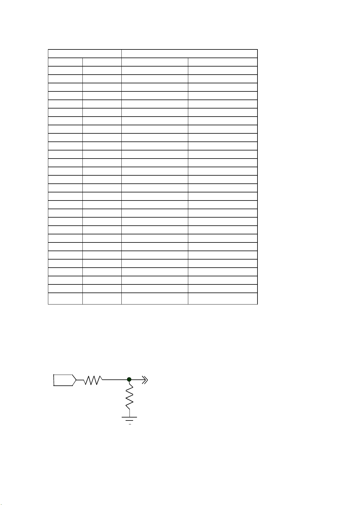
[Note 2] The equivalent circuit figure of the terminal
Ter mina l
1.0K ohm
10K ohm
Page 6
・Interface block diagram
Corresponding Transmitter: THC63LVDM83R (THine) or equivalent device
controller
G0
~
R0~R7
B0~B7
ENAB
G7
CLK
(
8
8
8
)
Rx1IN0+(13)
Rx1IN0-(12)
Rx1IN1+(16)
LVD S
↑
TTL
PLL
Rx1IN1-(15)
Rx1IN2+(19)
Rx1IN2-(18)
Rx1IN3+(25)
Rx1IN3-(24)
Rx1CLKIN+(22)
Rx1CLKIN-(21)
side
TV
・Block Diagram (LCD Module)
CN1
SOURCE/CONTROL PWB
Control Signals
SOURCE DRIVER
Power Supply
LCD PANEL
1366×3(RGB)×768
Circuit
TTL
↑
LVDS
PLL
(TFT-LCD side)
LD-K23Z03 -6
8
R0~R7
8
G0
G7
~
8
B0~B7
ENAB
CK
INPUT SIGNALS
CLKIN+
CLKINRIN0+
RIN0RIN1+
RIN1RIN2+
RIN2RIN3+
RIN3SELLVDS
POWER SUPPLY
+12V DC
Internal circuit s
GATE DRIVER
Page 7
SELLVDS= High (3.3V)
CLKIN+
CLKIN-
RIN0+
RIN0-
RIN1+
RIN1-
RIN2+
RIN2-
RIN3+
RIN3-
SELLVDS= Low(GND) or Open
CLKIN+
CLKIN-
RIN0+
RIN0-
RIN1+
RIN1-
RIN2+
RIN2-
RIN3+
RIN3-
DE: Display Enable
NA: Not Available (Fixed Low)
LD-K23Z03 -7
1 cycle
G2 R7 R6 R5 R4 R3 R2 R2 R3 G2
B3 B2 G7 G6 G5 G4 G3 G3 G4 B3
DE
NA NA
B1 B0 G1 G0 R1 R0 R0 R1 NA NA
B7 B6 B5 B4 B4 B5
DE
1 cycle
G0 R5 R4 R3 R2 R1 R0 R0 R1 G0
B1 B0 G5 G4 G3 G2 G1 G1 G2 B1
DE
NA NA
B7 B6 G7 G6 R7 R6 R6 R7 NA NA
B5 B4 B3 B2 B2 B3
DE
Page 8

LD-K23Z03 -8
V
V
4
F
2
2
4
5. Absolute Maximum Ratings
Parameter Symbol Condition Ratings Unit Remark
Input voltage
(for Control)
+12V supply voltage
(for Control)
I Ta=25°C -0.3 ~ 3.6 V [Note 1]
V
VCC Ta=25°C 0 ~ +15 V
Storage temperature Tstg - -25 ~ +60 °C
Operation temperature
(Ambient)
Topa - 0 ~ +50 °C
[Note 2]
[Note 1] SELLVDS
[Note 2] Humidity 95%RH Max.(Ta ≤ 40°C)
Maximum wet-bulb temperature at 39°C or less.(Ta > 40°C), No condensation.
6. Electrical Characteristics
6-1. Control circuit driving Ta=25°C
Parameter Symbol Min. Typ. Max. Uniit Remark
Supply voltage VCC +11.4 +12.0 +13.7 V [Note 1]
+12V supply
voltage
Current dissipation
ICC - 350 600 mA [Note 2]
I
- 1500 2500 mA [Note 5]
RUSH
T
RUSH
- 0.5 - ms [Note 5]
Permissible input ripple voltage VRP - - 100 mVP-P Vcc = +12.0V
High VTH - - 100 mV Differential input
threshold voltage
Low V
-100 - - mV
TL
Input Low voltage VIL 0 - 0.7 V
Input High voltage VIH 2.6 - 3.3 V
Input leak current (Low) IIL - - 400 µA
Input leak current (High) IIH - - 100 µA
V
CM = +1.2V
[Note 4]
[Note 3]
I = 0V
V
[Note 3]
I =3.3V
V
[Note 3]
Termi n al r e s i s t o r RT - 100 - Ω Differential input
[Note] VCM: Common mode voltage of LVDS driver.
[Note 1]
Input voltage sequences Dip conditions for supply voltage
50μs < t1 ≤ 20ms a) 9.1V ≤ V
< 10.8V
CC
20ms< t2-1 ≤ 5s td ≤ 10ms
20ms< t2-2 ≤ 5s b) V
< 9.1V
CC
0 < t3 ≤ 1s Dip conditions for supply voltage is
t4 ≥ 1s based on input voltage sequence.
t5 ≥ 300ms
0.9V
0.1VCC
CC
Data1
Data
Back light:
CC
t2-1
t1
t2-
t5
ON
INV
OFF
0.9 V
CC
0.1 VCC
t3
0.1V
t
OF
CC
V
9
.
7
1
.
V
2
td
Vcc
1
V
0
.
5
8
V
.
Page 9

LD-K23Z03 -9
※ Data1: CLKIN±,RIN0±,RIN1±, RIN2±, RIN3±
※ Data2: SELLVDS
※ About the relation between data input and back light lighting, please base on the above-mentioned input
sequence.
When back light is switched on before panel operation or after a panel operation stop, it may not display
normally. But this phenomenon is not based on change of an incoming signal, and does not give damage to a
liquid crystal display.
[Note 2]Typical current situation: 256 gray-bar pattern (V
= +12.0V)
CC
The explanation of RGB gray scale is seen in section 8.
RGB
GS0
RGB
GS1
RGB
GS2
....
RGB
GS254
RGB
GS255
V
= +12.0V
CC
CK = 82.0MHz
Th = 20.68μs
[Note 3] SELLVDS
[Note 4] CLKIN+/CLKIN-, RIN0+/RIN0-, RIN1+/RIN1-, RIN2+/RIN2-, RIN3+/RIN3-
[Note 5] The Rush current corrugation at the time of power on
Page 10

LD-K23Z03 -10
7. Timing characteristics of input signals
7-1. Timing characteristics
Timing diagrams of input signal are shown in Fig.2
Parameter Symbol Min.
Typ.
NTSC PAL
Max. Unit
Clock Frequency 1/Tc 72 82 82 85 MHz
Horizontal period TH
Data enable
signal
Horizontal period (High) THd 1366 1366 1366 1366 clock
Vertical period TV 778 806 967 972 line
Vertical period (High) TVd 768 768 768 768 line
[Note] When vertical period is very long, flicker may occur.
Please turn off the module after it shows the black screen.
Please make sure that length of vertical period should become of an integral multiple of horizontal length of
period. Otherwise, the screen may not display properly.
As for your final setting of driving timing, we will conduct operation check test at our side, please inform
your final setting.
Vertical period must change less than 1 line each flames.
TH
THd
DE
DATA
(R,G,B)
1366
1 2
Tc
1 2 768
DE
TV
Fig.2 Timing characteristics of input signals
1540 1696 1696 1940 clock
19.84 20.68 20.68 - µs
1366
767
TVd
Page 11

7-2. Input data signal and display position on the screen
R1 G1 B1 R2 G2 B2
(1、1) (1,2)
1・1 1・2 1・3
2・1 2・2
3・1
R G B
768・1
Display Position of Data (V,H)
1・1366
768・1366
LD-K23Z03 -11
Page 12

8. Input Signal, Basic Display Colors and Gray Scale of Each Color
Colors &
Gray scale
Gray
R0 R1 R2 R3 R4 R5 R6 R7 G0 G1 G2 G3 G4 G5 G6 G7 B0 B1 B2 B3 B4 B5 B6 B7
Scale
Data signal
LD-K23Z03 -12
Black
Blue
Green
Cyan
Red
Basic Color
Magenta
Yellow
White
Black GS0 0 0 0 0 0 0 0 0 0 0 0 0 0 0 0 0 0 0 0 0 0 0 0 0
GS1 1 0 0 0 0 0 0 0 0 0 0 0 0 0 0 0 0 0 0 0 0 0 0 0
×
Darker GS2 0 1 0 0 0 0 0 0 0 0 0 0 0 0 0 0 0 0 0 0 0 0 0 0
×
Ø
Brighter GS253 1 0 1 1 1 1 1 1 0 0 0 0 0 0 0 0 0 0 0 0 0 0 0 0
Gray Scale of Red
GS254 0 1 1 1 1 1 1 1 0 0 0 0 0 0 0 0 0 0 0 0 0 0 0 0
Ø
Red GS255 1 1 1 1 1 1 1 1 0 0 0 0 0 0 0 0 0 0 0 0 0 0 0 0
Black GS0 0 0 0 0 0 0 0 0 0 0 0 0 0 0 0 0 0 0 0 0 0 0 0 0
GS1 0 0 0 0 0 0 0 0 1 0 0 0 0 0 0 0 0 0 0 0 0 0 0 0
×
Darker GS2 0 0 0 0 0 0 0 0 0 1 0 0 0 0 0 0 0 0 0 0 0 0 0 0
×
Ø
Brighter GS253 0 0 0 0 0 0 0 0 1 0 1 1 1 1 1 1 0 0 0 0 0 0 0 0
Gray Scale of Green
GS254 0 0 0 0 0 0 0 0 0 1 1 1 1 1 1 1 0 0 0 0 0 0 0 0
Ø
Green GS255 0 0 0 0 0 0 0 0 1 1 1 1 1 1 1 1 0 0 0 0 0 0 0 0
0 0 0 0 0 0 0 0 0 0 0 0 0 0 0 0 0 0 0 0 0 0 0 0
-
0 0 0 0 0 0 0 0 0 0 0 0 0 0 0 0 1 1 1 1 1 1 1 1
-
0 0 0 0 0 0 0 0 1 1 1 1 1 1 1 1 0 0 0 0 0 0 0 0
-
0 0 0 0 0 0 0 0 1 1 1 1 1 1 1 1 1 1 1 1 1 1 1 1
-
1 1 1 1 1 1 1 1 0 0 0 0 0 0 0 0 0 0 0 0 0 0 0 0
-
1 1 1 1 1 1 1 1 0 0 0 0 0 0 0 0 1 1 1 1 1 1 1 1
-
1 1 1 1 1 1 1 1 1 1 1 1 1 1 1 1 0 0 0 0 0 0 0 0
-
1 1 1 1 1 1 1 1 1 1 1 1 1 1 1 1 1 1 1 1 1 1 1 1
-
È
È
È
È
È
È
È
È
È
È
È
È
È
È
È
È
Black GS0 0 0 0 0 0 0 0 0 0 0 0 0 0 0 0 0 0 0 0 0 0 0 0 0
GS1 0 0 0 0 0 0 0 0 0 0 0 0 0 0 0 0 1 0 0 0 0 0 0 0
×
Darker GS2 0 0 0 0 0 0 0 0 0 0 0 0 0 0 0 0 0 1 0 0 0 0 0 0
×
Ø
Brighter GS253 0 0 0 0 0 0 0 0 0 0 0 0 0 0 0 0 1 0 1 1 1 1 1 1
È
È
È
È
È
È
È
È
Gray Scale of Blue
GS254 0 0 0 0 0 0 0 0 0 0 0 0 0 0 0 0 0 1 1 1 1 1 1 1
Ø
Blue GS255 0 0 0 0 0 0 0 0 0 0 0 0 0 0 0 0 1 1 1 1 1 1 1 1
0 : Low level voltage, 1 : High level voltage.
Each basic color can be displayed in 256 gray scales from 8 bit data signals. According to the combination of total
24 bit data signals, the 16,777,216 colors display can be achieved on the screen.
Page 13

9. Optical characteristics
Parameter Symbol Condition Min. Typ. Max. Unit Remark
θ21
θ22
θ11
θ12
CR ≥ 10
70 88 - Deg.
70 88 - Deg.
Viewing angle
range
Horizontal
Vertical
Contrast ratio CRn 3750 5000 - -
Response time
Chromaticity of white
Chromaticity of red
Chromaticity of green
Chromaticity of blue
Luminance of white YL 320 400 - cd/m2
τ
DRV
x 0.252
y 0.258
x 0.604
θ=0 deg.
y 0.323
x 0.279
y 0.601
x 0.123
y
Luminance uniformity δW
- 7 - ms
0.031
0.282
0.288
0.634
0.353
0.309
0.631
0.153
0.061
0.312 -
0.318 -
0.664 -
0.383 -
0.339 -
0.661 -
0.183 -
0.091 -
- - 1.54 - [Note 6]
Measurement condition : Back Light Unit is used for LK315T3LWD0X.
*The measurement shall be executed 60 minutes after lighting at rating.
[Note] The optical characteristics are measured using the following equipment.
Detector (EZ-CONTRAST, Photo Diode)
400mm
Detector (SR-3)
Field=1°
Center of the screen (θ = 0°)
Center of the screen (θ = 0°)
TFT-LCD Module
TFT-LCD Module
Fig.3-1 Measurement of viewing angle range
and response time.
(Viewing angle range: EZ-CONTRAST
Response time: Photo Diode)
Fig.3-2 Measurement of Contrast,
Luminance, and Chromaticity.
LD-K23Z03 -13
Ta = 25°C, Vcc = +12V
[Note1,4]
[Note2,4]
[Note3,4,5]
[Note 4]
[Note 4]
Page 14

[Note 1] Definitions of viewing angle range :
LD-K23Z03 -14
Normal
θ11
θ21
θ12
θ22
6 o’clock direction
[Note 2] Definition of contrast ratio :
The contrast ratio is defined as the following.
Luminance (brightness) with all pixels white
Contrast Ratio
=
Luminance (brightness) with all pixels black
[Note 3] Definition of response time
The response time (τ
) is defined as the following figure and shall be measured by switching the input
DRV
signal for “any level of gray (0%, 25%, 50%, 75% and 100%)” and “any level of gray (0%, 25%, 50%, 75% and
100%)” at panel surface temperature 45°C.
0%
0%
25%
50%
75%
100%
td: 25%-0%
td: 50%-0% td: 50%-25%
td: 75%-0% td: 75%-25% td: 75%-50%
td: 100%-0% td: 100%-25% td: 100%-50% td: 100%-75%
25% 50% 75%
tr: 0%-25%
tr: 0%-50% tr: 0%-75% tr: 0%-100%
tr: 25%-50% tr: 25%-75% tr: 25%-100%
tr: 50%-75% tr: 50%-100%
t*:x-y...response time from level of gray(x) to level of gray(y)
= Σ(t*:x-y)/20
τ
DRV
[Note 4] This shall be measured at center of the screen.
[Note 5] This value is valid when O/S driving is used at typical input time value .
[Note 6] Definition of white uniformity ;
White uniformity is defined as the following with five measurements. (A~I)
Maximum luminance of Nine points (brightness)
W=
δ
Minimum luminance of Nine points (brightness)
100%
227 683 1139 画素
A
B
C
tr: 75%-100%
D
E
F
pixel
G
H
I
128
384
640
Page 15

LD-K23Z03 -15
10. Handling Precautions of the module
a) Be sure to turn off the power supply when inserting or disconnecting the cable.
b) Be sure to design the cabinet so that the module can be installed without any extra stress such as warp or
twist.
c) Since the front polarizer is easily damaged, pay attention not to scratch it.
d) Since long contact with water may cause discoloration or spots, wipe off water drop immediately.
e) When the panel surface is soiled, wipe it with absorbent cotton or other soft cloth.
f) Since the panel is made of glass, it may break or crack if dropped or bumped on hard surface. Handle with
care.
g) Since CMOS LSI is used in this module, take care of static electricity and take the human earth into
consideration when handling.
h) Please consider to minimize the influence of EMI and the exogenous noise before designing the grounding of
Open-Cell.
i) The Open-Cell has some printed circuit boards (PCBs) on the side, take care to keep them form any stress or
pressure when handling or installing the module; otherwise some of electronic parts on the PCBs may be
damaged.
j) Observe all other precautionary requirements in handling components.
k) When some pressure is added onto the module from rear side constantly, it causes display non-uniformity
issue, functional defect, etc.. So, please avoid such design.
l) When handling LCD modules and assembling them into cabinets, please be noted that long-term storage in
the environment of oxidization or deoxidization gas and the use of such materials as reagent, solvent,
adhesive, resin, etc. which generate these gasses, may cause corrosion and discoloration of the LCD
modules.
11. Reliability test item
No. Test item Condition
1 High temperature storage test Ta=60°C 500h
2 Low temperature storage test Ta=-25°C 500h
3
4
5
High temperature and high humidity
operation test
High temperature operation test Ta=50°C 500h
Low temperature operation test Ta=0°C 500h
Vibration test
6
(Cell Box with Open-Cells)
(non-operation)
Shock test
7
(Cell Box with Open-Cells)
(non-operation)
Ta=40°C ; 95%RH 500h
(No condensation)
(The panel surface temperature of this time is MAX60 ℃)
(The panel surface temperature of this time is MIN0 ℃)
X and Y direction: 15min, Z direction: 60min.
5Hz to 50Hz acceleration velocity: 1.0G
Sweeping ratio: 3min
Maximum acceleration: 490m/s
2
Pulse width: 11ms, sinusoidal half wave
Direction: +/-X, +/-Y, +/-Z, once for each direction.
Page 16

Page 17

Page 18

Page 19

Page 20

To: SHARP Corporation
pp
go.j
f
Report on Environmental Impact Substances Contained in Parts
and Materials
We guarantee the following verified results on the environmental impact substances:
1. Information on surveyed part:
1) Part Name
2) Sharp Part Code Number
3) Manufacturer’s Part Code Number
4) Part(Material) Weight (g)
TFT Open-Cell
R1LK315T3HB00X
LK315T3HB00X/T/A
1200g
Date:
Company Name:
Department:
Jan,06,2012
1/1
SHARP CORPRATION
LIQUID CRYSTAL DISPLAY GROUP
2. Ozone-depleting substances contained in the part or used in manufacturing:
No. Substances
Ozone-depleting substances(regulated by the
1
Montreal Protocol (Class I and II))(*1)
Note: When the verified results show the substances are “present”, the part or material is prohibited by the SHARP standard.
Not contained in part/materials. However, use of the refrigerant (HCFC) for
air-conditioners is considered as object exclusion.
Not used in the rinse process. (Object: PWBs, )
(Even if you select "Not use" that means you didn’t use these substances to rinse
process, you have to describe rinse solution and method of the rinse process.)
Details (Criteria)
3. Presence of banned substances in the part (material)
No. Substances
Hexavalent chromium compound Content is 1000ppm or less. Not intentionally added. (*3)
1
Bis(tri-n-butyltin) oxide
2
Tri-substiituted organostannic compounds Content is 1000ppm or less. Not intentionally added.
3
Polybrominated biphenyls (PBBs)
4
Polybrominated diphenyl ethers
5
(PBDEs)
Polychlorinated biphenyls (PCBs)
13
6
Polychlorinated naphthalene
7
Short chain chlorinated paraffin Not intentionally added. (Only C:10-13 are subject to the regulation.)
8
Asbestos Not intentionally added.
9
Polychlorinated Terphenyls (PCTs)
10
Phenol,2-(2H-benzotriazol-2-yl)-4,6-
11
bis(1,1-dimethylethyl)
Tris (2-chloroethyl) phosphate
12
Hexabromocyclododecane
Diarsenic Pentoxide
14
Cobalt dichloride
15
Dimethyl fumarate
16
Refractory Ceramic Fibres,Aluminosilicate
17
Refractory Ceramic Fibres,
18
Zirconia Aluminosilicate
Note: When the verified results show the substances are “present”, the part or material is prohibited by the SHARP standard.
Content is 1000ppm or less. Not intentionally added. Not present
Content is 1000ppm or less. Not intentionally added. Not present
Content is 1000ppm or less. Not intentionally added.
Not intentionally added. Not present
Not intentionally added.(Only poly chlorinated naphthalene with
three chlorines and more is subject to the regulation.)
Not intentionally added. Not present
Not intentionally added.
Content is 1000ppm or less. Not intentionally added. Not present
Content is 1000ppm or less. Not intentionally added. Not present
Content is 1000ppm or less. Not intentionally added. Not present
Content is 1000ppm or less. Not intentionally added. Not present
Content is 1000ppm or less. Not intentionally added. Not present
Not intentionally added. Not present
Not intentionally added. Not present
Details (Criteria) (*2) Verified Result
Verified Result
Not present
Not use/Use
Rinse solution:
Rinse method:
Not present
Not present
Not present
Not present
Not present
Not present
Not present
Not present
Not present
Not present
4. Presence of banned substances depending on application
When the verified result of criteria shows the substances are "present",
please complete and return the “CONFIRMATION OF USE” form which details use of each substance.
No. Substances
Cadmium and its compound Content is 100ppm or less. Not intentionally added. (*3)
1
Lead and its compound Present
2
Mercury and its compound Content is 1000ppm or less. Not intentionally added. (*3)
3
Beryllium and its compound Content is 1000ppm or less. Not intentionally added.
4
Azo colorants Not intentionally added. Content is 30ppm or less.
5
Polyvinyl Chloride Not intentionally added.
6
Phthalates Content is 1000ppm or less. Not intentionally added.
7
Radioactive substances Not intentionally added.
8
Perfluorooctane sulfonate(PFOSs)
9
and its salt(*4)
Formaldehyde
10
Nickel
11
Perchlorates Not intentionally added.(The object of survey is only battery)
12
Diarsenic trioxide Content is 1000ppm or less. Not intentionally added.
13
Arsenic and its compound (except Diarsenic
14
Pentoxide and Diarsenic trioxide)
Boric acid Content is 1000ppm or less. Not intentionally added.
15
Disodium tetraborate,anhydrous
16
Tetraboron disodium heptaoxide, hydrate
Dibutyltin (DBT) compounds Content is 1000ppm or less of tin in a material. Not Intentionally added.
17
Dioctyltin (DOT) compounds Content is 1000ppm or less of tin in a material. Not Intentionally added.
18
*1) Regarding Ozone-depleting substances, object substances are CFC, 1,1,1-trichloroethane, Carbon tetrachloride, Bromomethane,Halon HBFC, and HCFC.
*2) Unit for calculating content rate is homogenious material.
*3) For packaging part and packaging material, the total concentration of these 4 heavy metals in part/material, ink and paint which constitute a package
is 100ppm or less each.
*4) Concerning "Perfluorooctane sulfonate(PFOSs) and its salt", please refer to the Web Site of Ministry of Economy, Trade and Industry of Japan.
URL: http://www.meti.
*5) When the verified result shows the substances are "present", please complete and return the attachment 1 “CONFIRMATION OF USE FORM” which details use of
each substance.
p/policy/chemical_management/03kanri/96list.pd
Approved:
Not intentionally added. Content in plastics is 300ppm or less.
Content in others is 1000ppm or less. (*3)
Not intentionally added, and Content in substance/preparation is 50ppm or less,
content of sub-product/article etc. except substance/preparation is
m or less, content of coating agent is 1μg/m2 or less.
1000
Wood component: atmospheric concentration is 0.1ppm or less
(by the chamber method).
Plastics/fibers: content is 75ppm or less.
Not intentionally added. Present
Content is 1000ppm or less. Not intentionally added.
Content is 1000ppm or less. Not intentionally added.
SHIGEKI TANAKA
Details (Criteria)(*2) Verified Result(*5)
Written by:
YOSHITAKE NAKAMURA
Not present
Not present
Present
Present
Not present
Not present
Not present
Not present
Not present
Not present
Not present
Not present
Not present
Not present
Not present
Not present
Not present
Not present
Not present
Not present
Not present
Not present
Signature: Signature:
Ver.5.3 Revised: June, 2011
Page 21

y
To: SHARP Corporation
Attachement 1 "CONFIRMATION OF USE FORM"
(Parts and materials which are usable or prohibited according to application)
This form is to be completed when the verified results in the form 'Report on Environmental Impact Substances Contained in Parts
and Materials' have shown the presence of banned substances with restrictions depending on application.
1. Information on survey applicable part
1) Part Name TFT Open-Cell
2) Sharp Part Code Number R1LK315T3HB00X
3) Manufacturer’s Part Code Number LK315T3HB00X/T/A
2.Detail of verified result
Please indicate with a "O" in the verified results column if an
of the restricted substances are used for the following reasons.
No. Substances Check point ( criteria )
(1) Used for electric point
Cadmium
1
and its compound
Lead
2
and its compound
Mercury
3
and its compound
Beryllium and its
4
compound
5 Azo colorants
6 Polyvinyl Chloride
7 Phthalate esters
Radioactive
8
substances
Perfluorooctane
9
sulfonate(PFOSs)
and its salt
10 Formaldehyde
11 Nickel
12 Perchlorates
13 Diarsenic trioxide
Arsenic and
14
its compound
15 Boric acid
Disodium tetraborate,
anhydrous Tetraboron
16
disodium heptaoxide,
hydrate
Dibutyltin (DBT)
17
compounds
Dioctyltin (DOT)
18
compounds
Note: When the verified results correspond to "banned", the part or material is prohibited by the SHARP standard.
(2) Used in filter glass.
(3) Used in a thermal cutoff of a one shot pellet type
(4) Battery is compliant with the EU Battery Directive (98/101/EC).
(5) Used in every application other than the above (1-4).
(1) Used in high-melting point solder (lead-based alloys containing 85 % by weight or more lead)
(2) Used in electrical and electronic components in a glass or ceramic other than dielectric ceramic in capacitors,
(3) Used less than 0.2% by weight in glass of a fluorescent tube
(4) Contained in alloy component. (Lead content should be less than 0.35 Wt%, 0.4 Wt% and 4Wt% in steel material,
aluminum material and copper material, respectively.)
(5) Used in solder consisting of more than two types of elements for connecting microprocessor pins and package containing
(6) Used in solder for connecting semiconductor dies and carriers in flip chip IC packages
(7) Used in white glass or filter glass used for an optical purpose
(8) Used in coating material for thermal conduction module C-rings
(9) Used in shell (exterior casing) or bushing (a cylindrical component fitted inside a hole) of a bearing for a compressor
(10) Used in dielectric ceramic used in a capacitor with rated voltage of 125V AC or 250V DC or larger
(11) Used in a dielectric ceramic used in a capacitor with rated voltage less than 125V AC or 250V DC
(12) Used in glass used for flat fluorescent lamps used for LCD, designing, or lighting for industrial purpose
(13) Used in finishing agents of 0.65 mm or finer pitch components other than connectors
(14) Used for stabilizer or additive for non-electrolytic gold or nickel plating
(15) Battery is compliant with the EU Battery Directive (98/101/EC).
(16) Used in products for children 12 and under, containing lead exceeding 300ppm per surveying unit.
(17) Used in parts/material used in toys, containing lead above 0.009% per surface treatment layer such as coating.
(18) Used in the other than the above (1-15).
(1) Used in single-capped fluorescent lamp that does not exceed the following limitations (per burner):
(a) For general illumination less than 30W: 5mg, (b) For general illumination of 30W or higher and less than 50W: 5 mg
(c) For general illumination of 50W or higher and less than 150W: 5 mg, (d) For general illumination of 150W or higher: 15mg
(e) Having a circular or square structure, 17mm or less in tube diameter, and for general illumination: 7mg, (f) For a specific use: 5 mg
(2) Used in double-capped strip fluorescent lamp (in each lamp) for general purposes that does not exceed the following limitations:
(a) A three-wavelength phosphor of less than 9mm in tube diameter (e.g., T2) with normal lifetime: 5mg
(b) A three-wavelength phosphor of 9mm or larger and of 17mm or less in tube diameter (e.g., T5) with normal lifetime: 5mg
(c) A three-wavelength phosphor of over 17mm and 28mm or less in tube diameter (e.g., T8) with normal lifetime: 5mg
(d) A three-wavelength phosphor of over 28mm in tube diameter (e.g., T12) with normal lifetime: 5mg
(e) A three-wavelength phosphor with long lifetime (> 25,000 h) : 8mg
(3) Used in double-capped fluorescent lamp (in each individual lamp) not for general purposes under the following conditions:
(a) A linear white lamp of 28mm in tube diameter (e.g., T10 and T12): mercury that does not exceed 10mg
(b) Nonlinear white lamps of all shapes: mercury that does not exceed 15mg
(c) Mercury contained in a nonlinear three-wavelength phosphor lamp of 17mm or larger (e.g., T9)
(d) Mercury contained in a lamp for any other general illumination or specific purposes (e.g., induction lamps)
(4) Used in cold cathode fluorescent lamps and external electrode fluorescent lamps (CCFL and EEFL)
for special purposes not exceeding (per lamp):
(a)Short length (≤ 500 mm): 3.5mg, (b)Medium length (> 500 mm and ≤ 1500 mm): 5mg, (c)Long length (> 1500 mm): 13mg
(5) Used in low pressure discharge lamps (per lamp) other than the above(1-4)
(6) Used in extra-high voltage sodium (vapor) lamp for general illumination with an improved color rendering index over 60
(7) Used in extra-high voltage sodium (vapor) lamp for general illumination
(8) Used in high-pressure mercury vapor lamp (HPMV)
(9) Used in high-pressure mercury vapor lamp (HPMV)
(10) Used in metal halide lamp (MH)
(11) Battery is compliant with the EU Battery Directive (98/101/EC).
(12) Used in every application other than the above (1-11).
(1) Used in the exception items. (exception items: alloy, ceramics, glass, semiconductor)
(2) Used in the parts excluding exception items
(1) Used in a contact part with human body of a product (ex:electric carpet, earphone, strap and etc.) which is manufactured
based on the premise that the product continuously contacts human body, and may produce amine when discomposed.
(2) Used in every application other than the above (1). (Used in a part which does not continuously contact with human body.)
(1) Used in packaging material and packaging part for Sharp product.
(2) Used for the other than the above (1).
(1) Bis(2-ethylhexyl)phthalate:DEHP/DOP is used intentionally.
(2) Dibutyl phthalate:DBP, or Bis(butylbenzyl) phthalate:BBP, or Diisobutyl phthalate:DIBP is used.
(3) Dinonyl phthalate:DINP, or Diisodecyl phthalate:DIDP, or Di-n-octyl phthalate:DNOP is used
in parts/materials that is used in products for children 12 and under.
(4) Bis(2-ethylhexyl)phthalate:DEHP/DOP is contained as impurities (Not intentionally added)
(5) Used in the other than the above (1-3).
(1) Used in the magnetron of a microwave oven. (Only Thorium is subject to the regulation.)
(2) Used in the electric bulb of a LCD projector. (Only Krypton 85 is subject to the regulation.)
(3) Used in the other than the above (1-2).
(1)Used in photoresists and rantireflection coating for the photolithography process.
(2) Used in photo coating used in pringing plates, film, and documents.
(3) Used in mist suppressants for hard chrome plating, and moistening agent used in equipment for plating.
(4) Used in every application other than the above (1-3).
(1) Used in wooden parts.
(2) Used in a direct human body contact part of a product which is intended to continuously contact with human body.
(ex: electric carpet, earphone, strap and etc.)
(3) Used in every application other than the above (1-2).
(1) Used in parts which continuously contact with human skin for a long time.
(2) Used in the other than the above (1).
(1) Contained above 6ppb by weight per battery
(2) Contained less than 6ppb by weight per battery
(1) Used in the lamp of LCD projector.
(2) Used in the other than the above (1).
(1) Used for the exception items. (exception items: semiconductor, resist, magnet filter, copper foil and battery)
(2) Used in the other than the above (1).
(1) Used in the polarizers(made of PVA) of LCD panel and glass.
(2) Used in adhensive agent.
(3) Used for the other than the above (1-2).
(1) Used in the polarizers(made of PVA) of LCD panel and glass.
(3) Used for the other than the above (1-2).
(1) Used for one-component and two-component room temperature vulcanisation sealants (RTV-1 and RTV-2 sealants) and adhesives
(2) Used for paints and coatings containing DBT compounds as catalysts when applied on articles
(3) Used in stabilizer of soft polyvinyl chloride (PVC) for outdoor purpose
(4) Used in catalyst for polymerization of resin for toner. Content as a metal tin is 1000ppm or less.
(5) Used for the other than the above (1-4).
(1) Used for two-component room temperature vulcanisation moulding kits (RTV-2 moulding kits)
(2) Used for the other than the above (1).
Approved:
SHIGEKI TANAKA
less than 85wt% and more than 80wt% of lead.
containing coolant for heating,ventilation, air-conditioning, refrigeration, chilling, and HVACR
(2) Used in adhensive agent and fibers.
Signature: Signature:
e.g. piezoelectronic devices, or in a glass or ceramic matrix compoundcompounds
Written by:
Date: Jan,06,2012
Company Name:
Verified Adaptability under the
Results SHARP standard
SHARP CORPRATION
Department:
LIQUID CRYSTAL DISPLAY GROUP
○
○
○
○
○
○
○
YOSHITAKE NAKAMURA
Usable
Banned
Usable
Banned
Usable
Banned
Usable
Banned
Banned
Usable
Banned
Usable
Banned
Usable
Usable
Banned
Usable
Banned
Banned
Usable
Banned
Usable
Usable only with
statement
Usable
Usable
Banned
Usable
Banned
Usable
Banned
Usable
Banned
Usable
Banned
Banned
Usable
1/1
Ver.5.3 Revised: June, 2011
 Loading...