

Page 1
Page 2
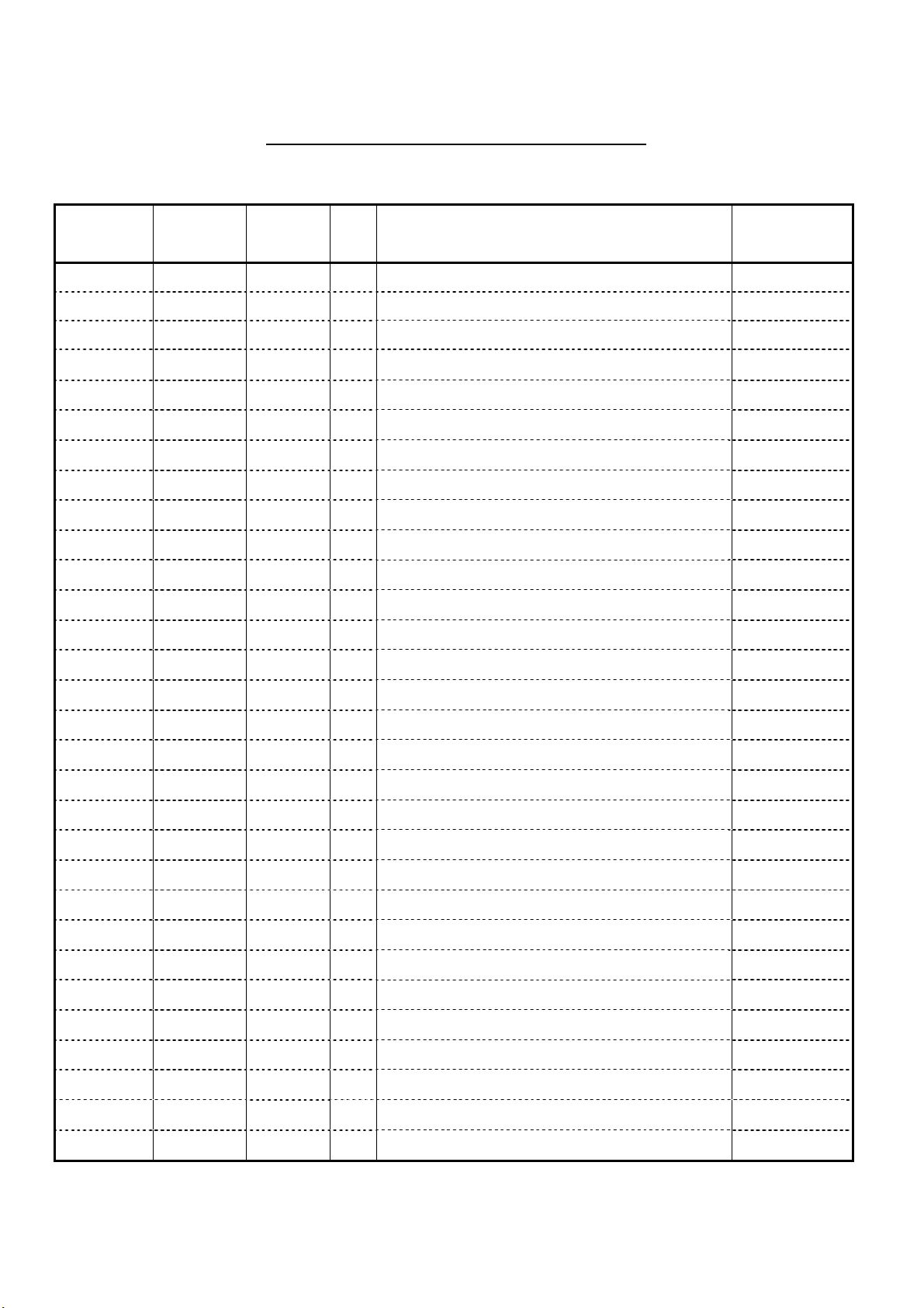
RECORDS OF REVISION
MODEL No. : LK315T3HA2M
SPEC No. :
DATE
NO.
2010.11.10
LD-K22Y09
LD-K22Y09
REVISED
No.
PAGE SUMMARY NOTE
- - - 1st Issue
Page 3
LD-K22Y09-1
r
1. Application
This technical literature applies to the color 31.5” TFT-LCD Open-Cell (LK315T3HA2M).
* This technical literature is proprietary product of SHARP CORPORATION (“SHARP”) and includes materials
protected under copyright of SHARP. Do not reproduce or cause any third party to reproduce them in any form or by
any means, electronic or mechanical, for any purpose, in whole or in part, without the express written permission of
SHARP.
* In case of using the device for applications such as control and safety equipment for transportation (aircraft, trains,
automobiles, etc.), rescue and security equipment and various safety related equipment which require higher
reliability and safety, take into consideration that appropriate measures such as fail-safe functions and redundant
system design should be taken.
* Do not use the device for equipment that requires an extreme level of reliability, such as aerospace applications,
telecommunication equipment (trunk lines), nuclear power control equipment and medical or other equipment for
life support.
* SHARP assumes no responsibility for any damage resulting from the use of the device that does not comply with
the instructions and the precautions specified in this technical literature.
* Contact and consult with a SHARP sales representative for any questions about this device.
2. Overview
This Open-Cell is a color active matrix LCD panel incorporating amorphous silicon TFT (Thin Film Transistor). It
is composed of a color TFT-LCD panel, driver ICs, Source-Control and Source-PWB.
Graphics and texts can be displayed on a 1366×RGB×768 dots panel with 16,777,216 colors by using LVDS (L
oltage Differential Signaling) for the interface and +12V DC supply voltage, which are put into Source-Control
V
PWB.
This applies the Over Shoot driving (O/S driving) technology, signals are being applied to the Liquid Crystal
according to a pre-fixed process as image signals of the present frame when a difference is found between image
signals of the previous and current frame by comparing each other. The O/S driving technology makes the Liquid
Crystal response within 1 frame completely, motion blur reduce, so that clearer display performance can be realized.
ow
3. Mechanical specifications
Paramete
Display size
Active area 697.69 (H) × 392.26 (V) mm
Pixel Format
Pixel pitch
Pixel configuration
Display mode
Outline Dimensions [Note1]
Mass
Surface treatment [Note2]
(Polarizer)
[Note1] Outline dimensions are shown in P18.
[Note2] Without the protection film.
80.039 (Diagonal)
31.5 (Diagonal)
1366 (H) × 768 (V)
(1pixel = R + G + B dot)
0.51075(H) × 0.51075 (V)
R,G, B vertical stripe
Normally black
716.7(W) × 447.6(H) × 1.8(D)
1.15±0.1
Low-Haze Anti Glare, Hard coating
Surface Hardness;
2H: CF side (Front)
<6B: TFT side (Rear)
Specifications Unit
cm
inch
pixel
mm
mm
kg
Page 4
Interface specifications
4.
4.1. TFT panel driving
CN1 (Interface signals and +12V DC power supply; shown in Fig.1)
Used connector: GT103-30S-H23-D-E2500 (LSMtron)
Mated connector: FI-X30H/FI-X30HL, FI-X30C/FI-X30C2L
Mated LVDS transmitter: THC63LVDM83R (THine) or equivalent device
Pin No. Symbol Function Remark
1 VCC +12V Power Supply
2 VCC +12V Power Supply
3 VCC +12V Power Supply
4 VCC +12V Power Supply
5 GND
6 GND
7 GND
8 GND
9 SELLVDS
10 Reserved
11 GND
12 RIN013 RIN0+
14 GND
15 RIN116 RIN1+
17 GND
18 RIN219 RIN2+
20 GND
21 CLKIN22 CLKIN+
23 GND
24 RIN325 RIN3+
26 GND
27 Reserved
28 Reserved
29
30
[Note] GND of a liquid crystal panel drive part has connected with a module chassis.
or FI-X30M (Japan Aviation Electronics Ind. , Ltd.)
Ground
Ground
Ground
Ground
Select LVDS data order [Note 1]
Not Available
Ground
Negative (-) LVDS differential data input
Positive (+) LVDS differential data input
Ground
Negative (-) LVDS differential data input
Positive (+) LVDS differential data input
Ground
Negative (-) LVDS differential data input
Positive (+) LVDS differential data input
Ground
Clock Signal(-)
Clock Signal(+)
Ground
Negative (-) LVDS differential data input
Positive (+) LVDS differential data input
Ground
Not Available
Not Available
GND
GND
Ground
Ground
LD-K22Y09-2
Default: Pull down
(L:GND)
[Note 2]
LVDS
LVDS
LVDS
LVDS
LVDS
LVDS
LVDS
LVDS
LVDS
LVDS
Page 5
[Note1] LVDS data order
Transmitter SELLVDS
Pin No Data
51 TA0
52 TA1
54 TA2
55 TA3
56 TA4
3 TA5
4 TA6
6 TB0
7 TB1
11 TB2
12 TB3
14 TB4
15 TB5
19 TB6
20 TC0
22 TC1
23 TC2
24 TC3
27 TC4
28 TC5
30 TC6
50 TD0
2 TD1
8 TD2
10 TD3
16 TD4
18 TD5
25 TD6
=L(GND) or Open
R0(LSB)
R1
R2
R3
R4
R5
G0(LSB)
G1
G2
G3
G4
G5
B0(LSB)
B1
B2
B3
B4
B5
NA NA
NA NA
DE(*) DE(*)
R6 R0(LSB)
R7(MSB) R1
G6 G0(LSB)
G7(MSB) G1
B6 B0(LSB)
B7(MSB) B1
NA NA
= H(3.3V)
R2
R3
R4
R5
R6
R7(MSB)
G2
G3
G4
G5
G6
G7(MSB)
B2
B3
B4
B5
B6
B7(MSB)
LD-K22Y09-3
NA: Not Available
(*) Since the display position
is prescribed by the rise of DE (Display Enable) signal,
please do not fix DE signal at "High " during operation.
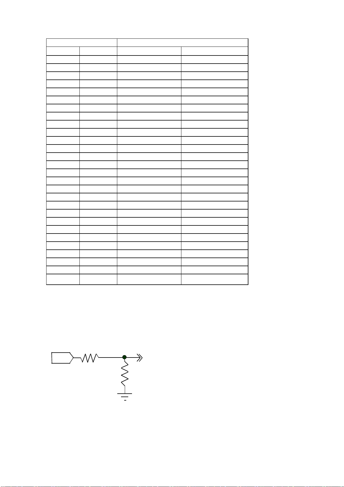
[Note 2] The equivalent circuit figure of the terminal
Ter mina l
1.0K ohm
10K ohm
Page 6
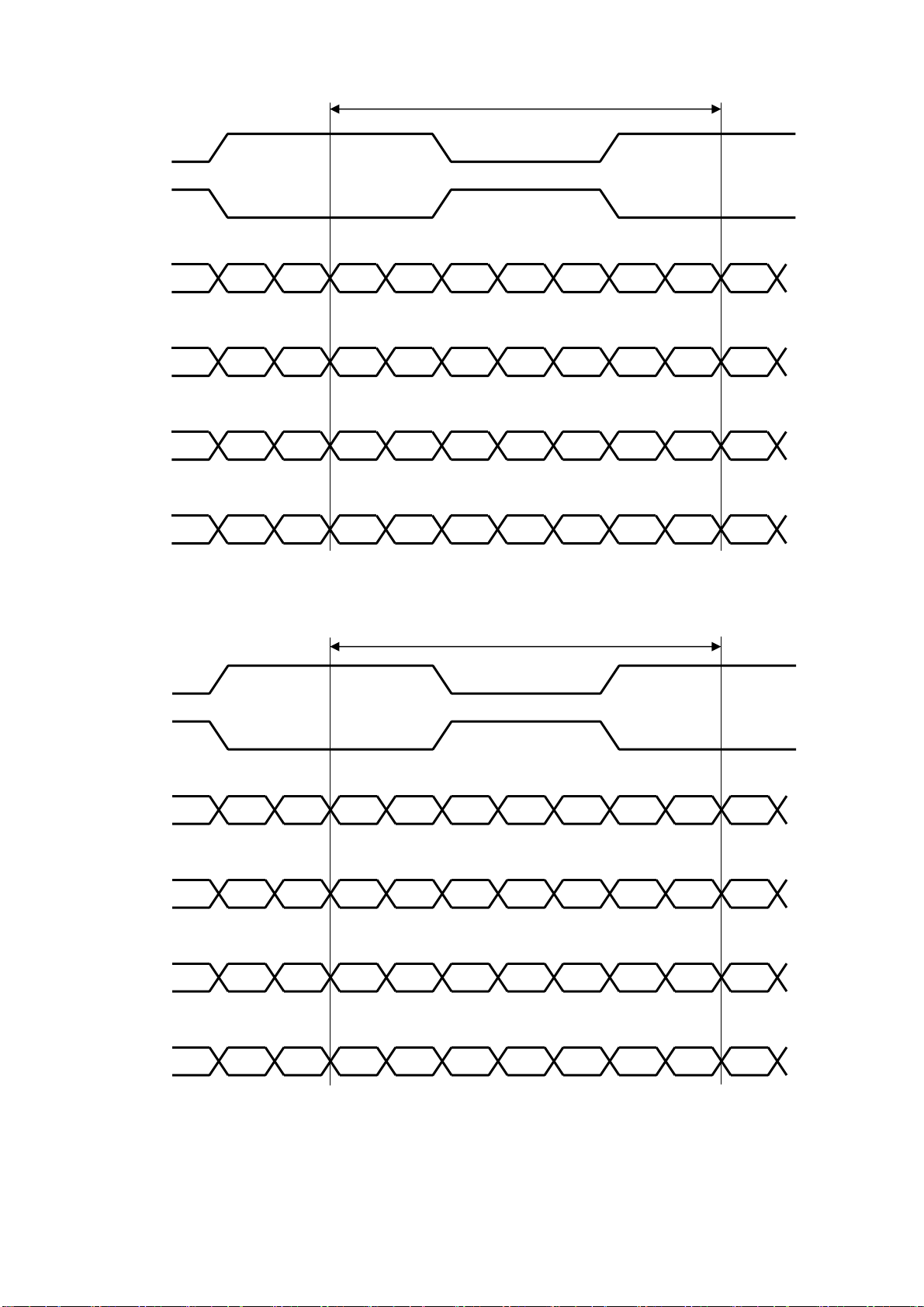
SELLVDS= High (3.3V)
CLKIN+
CLKIN-
RIN0+
RIN0-
RIN1+
RIN1-
RIN2+
RIN2-
RIN3+
RIN3-
SELLVDS= Low (GND) or Open
CLKIN+
CLKIN-
RIN0+
RIN0-
RIN1+
RIN1-
RIN2+
RIN2-
RIN3+
RIN3-
DE: Display Enable
NA: Not Available (Fixed Low)
LD-K22Y09-4
1 cycle
G2 R7 R6 R5 R4 R3 R2 R2 R3 G2
B3 B2 G7 G6 G5 G4 G3 G3 G4 B3
DE
NA NA
B1 B0 G1 G0 R1 R0 R0 R1 NA NA
B7 B6 B5 B4 B4 B5
DE
1 cycle
G0 R5 R4 R3 R2 R1 R0 R0 R1 G0
B1 B0 G5 G4 G3 G2 G1 G1 G2 B1
DE
NA NA
B7 B6 G7 G6 R7 R6 R6 R7 NA NA
B5 B4 B3 B2 B2 B3
DE
Page 7
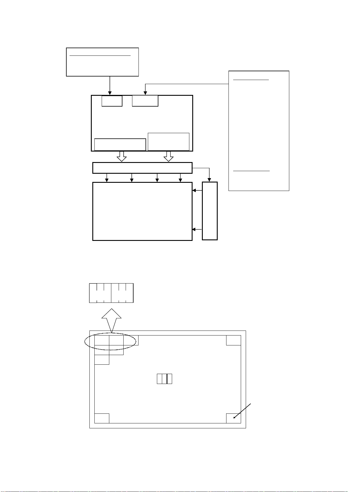
4.2. Interface block diagram
VCOM Control signals
CTL
CE
CN201
Control signals
4.3. Display position of data
R1 G1 B1 R2 G2 B2
(1、1) (1,2)
CN1
Source-Control PWB
Power supply
circuit
Source driver
LCD panel
1366×3(RGB)×768
Fig.1 Interface block diagram
Input signals
Power supply
+12V DC
Gate driver
LD-K22Y09-5
CLKIN+
CLKINRIN0+
RIN0RIN1+
RIN1RIN2+
RIN2RIN3+
RIN3SELLVDS
1・1 1・2 1・3
2・1 2・2
3・1
R G B
768 ・1
Display Position of Data (V,H)
1・13 6 6
768・1366
Page 8

4.4.
Vcom Adjusting interface of Source-Control PWB
CN201 (Interface Vcom Adjusting) in Source-Control PWB
Using Via Hole : 1.5mm Pitch (φ0.7mm )
Mated connector : (housing) 5P-SZN, (contact) SZN-002T-P0.7K (JST Co., Ltd.)
Communication method
Pulse control method
:
Pin No. Symbol Function Remark
1 NC
2 NC -
3 GND Signal GND
4 CTL
Control Signal [Note1]
5 CE Chip Enable [Note1] Pull down to GND [Note2]
[Note1] Refer to specifications of MAX1512 (MAXIM) for Vcom adjustment.
You should adjust a flicker to be minimized in below pattern, where the gray level of “0” and “127” are
displayed alternately at every subpixel, otherwise images may be remained on the screen.
[Note2] The equivalent circuit figure of the terminal is as below:
Ter mi na l
100 [Ω]
30K [Ω]
R G B R G B G B
(1,1)
GS0
GS127
GS0
GS127
GS0
GS127
GS0
GS127
GS127
GS0
GS0
GS127
GS127
GS0
Equivalent circuit of CE terminal
GND
(1,768)
GS127
GS0
Flicker-Check Pattern
Absolute maximum ratings
5.
Parameter Symbol Condition Ratings Unit Remark
Input voltage
(for Source-Control PWB)
+12V supply voltage
(for Source-Control PWB)
I Ta=25°C -0.3 ~ 3.6 V [Note 1]
V
Ta=25°C 0 ~ +15 V
V
CC
LD-K22Y09-6
GS127
GS0
GS127
GS127
GS0
GS0
(1366,1)
(1366,768)
Vcom control voltage V
Ta=25°C -0.3 ~ +1 6 V
CTL
Storage temperature Tstg - -25 ~ +60 °C
Operation temperature
(Ambient)
Topa - 0 ~ +50 °C
[Note 1] SELLVDS
[Note 2] Humidity 95%RH Max.(Ta 40°C)
Maximum wet-bulb temperature is 39°C or less (Ta > 40°C). No condensation.
[Note 2]
Page 9

LD-K22Y09-7
V
C
0
4
Electrical characteristics
6.
6.1. Electrical characteristics of input signals
Ta=25°C
Parameter Symbol Min. Typ. Max. Uniit Remark
+11.4 +12.0 +12.6 V [Note 1]
CC
- 330 600 mA [Note 2]
I
CC
I
- 1100 2500 mA [Note 5]
RUSH
T
RUSH
- 0.5 - ms [Note 5]
+12V supply
voltage
Supply voltage V
Current
consumption
Permissible input ripple voltage VRP - - 100 mVP-P Vcc = +12.0V
Differential input
threshold voltage
Input low voltage VIL 0 - 0.7 V
Input high voltage VIH 2.6 - 3.3 V
Input leak current (Low) IIL - - 400 µA
Input leak current (High) IIH - - 100 µA
High VTH - - 100 mV
Low VTL -100 - - mV
CM = +1.2V
*V
[Note 4]
[Note 3]
I = 0V
V
[Note 3]
I =3.3V
V
[Note 3]
Terminal resistor RT - 100 - Ω Differential input
[Note] *VCM: Common mode voltage of LVDS driver.
[Note 1]
Input voltage sequences Dip conditions for supply voltage
0 < t1 20ms a) 9.1V V
< 10.8V
CC
20ms< t2-1 td 10ms
20ms< t2-2 b) VCC < 9.1V
0 < t3 1s Dip conditions for supply voltage is
t4 1s based on input voltage sequence.
t5 300ms
.9VCC
0.1 V
CC
V
C
t1
Data1
Data2
Back li ght: V IN
t2-1
t2-2
0.9 VCC
0.1VCC
t3
t5
ON
0.1 V
t4
OFFOFF
CC
V
9
.
7
1
.
V
2
td
Vcc
1
V
0
.
5
8
V
.
※ Data1: CLKIN±,RIN0±,RIN1±, RIN2±, RIN3±
※ Data2: SELLVDS
※ About the relation between data input and back light lighting, we recommend the above-mentioned input
sequence.
If the back light is switched on before a panel operation begins or after a panel operation stops, the screen may
not be displayed properly. But this phenomenon is not caused by change of an incoming signal, and does not
give damage to a liquid crystal display.
Page 10

[Note 2]Typical current situation: 256 gray-bar pattern (V
= +12.0V)
CC
The explanation of RGB gray scale is seen in section 8.
RGB
GS0
RGB
GS1
RGB
GS2
....
RGB
GS254
RGB
GS255
VCC = +12.0V
CK = 82.0MHz
Th = 20.68μs
[Note 3] SELLVDS
[Note 4] CLKIN+/CLKIN-, RIN0+/RIN0-, RIN1+/RIN1-, RIN2+/RIN2-, RIN3+/RIN3-
[Note 5] The rush current corrugation at the time of power on
5msec
LD-K22Y09-8
0.9Vcc
0.1Vcc
T
RUSH
I
RUSH
(Max)
Vcc
I
(500mA/div)
RUSH
4ms/div
Page 11

LD-K22Y09-9
6.2.
Timing characteristics of input signals
Timing diagrams of input signal are shown in Fig.2
Parameter Symbol Min. Typ. Max. Unit
Clock Frequency 1/Tc 72 82 85 MHz
1540 1696 1940 clock
Horizontal period TH
19.84 20.68 - µs
Data enable
signal
Horizontal period (High) THd 1366 1366 1366 clock
Vertical period TV 778 806 972 line
Vertical period (High) TVd 768 768 768 line
[Note] *When a vertical period is very long, a flicker may occur.
*Please turn off the module after it shows the black screen.
*Please make sure that a length of vertical period should be an integral multiple of horizontal period,
otherwise the screen may not display properly.
*Please be careful not to fall below the minimum horizontal period, otherwise the display may be dark.
We will check the display operation for your final setting of drive timing, so please inform us of your final setting.
TH
THd
DE
DATA
(R,G,B)
1366
1 2
1366
Tc
1 2 768
767
DE
TV
TVd
Fig.2 Timing diagram of input signals
Page 12

LD-K22Y09-10
6.3.
CLK-
CLK+
LVDS signal characteristics
RINx-
RINx+
tpd0
t
CLK
Vdiff=0 Vdiff=0
tpd1
tpd2
tpd3
tpd4
tpd5
tpd6
Data
position
The item Symbol min. typ. max. unit
Delay time, CLK rising edge
tpd0
-0.40 0 0.40
to serial bit position 0
Delay time, CLK rising edge
tpd1
typ-0.40
1* t
CLK
/7
typ+0.40
to serial bit position 1
Delay time, CLK rising edge
tpd2
typ-0.40
2* t
CLK
/7
typ+0.40
to serial bit position 2
Delay time, CLK rising edge
tpd3
typ-0.40
3* t
CLK
/7
typ+0.40
to serial bit position 3
Delay time, CLK rising edge
tpd4
typ-0.40
4* t
CLK
/7
typ+0.40
to serial bit position 4
Delay time, CLK rising edge
tpd5
typ-0.40
5* t
CLK
/7
typ+0.40
to serial bit position 5
Delay time, CLK rising edge
tpd6
typ-0.40
6*
t
/7
CLK
typ+0.40
to serial bit position 6
ns
Page 13

Input signal, basic display colors and gray scale of each color
7.
Colors &
Gray scale
Gray
R0 R1 R2 R3 R4 R5 R6 R7 G0 G1 G2 G3 G4 G5 G6 G7 B0 B1 B2 B3 B4 B5 B6 B7
Scale
Data signal
LD-K22Y09-11
Black
Blue
Green
Cyan
Red
Basic Color
Magenta
Yellow
White
Black GS0 0 0 0 0 0 0 0 0 0 0 0 0 0 0 0 0 0 0 0 0 0 0 0 0
GS1 1 0 0 0 0 0 0 0 0 0 0 0 0 0 0 0 0 0 0 0 0 0 0 0
Darker GS2 0 1 0 0 0 0 0 0 0 0 0 0 0 0 0 0 0 0 0 0 0 0 0 0
Brighter GS253 1 0 1 1 1 1 1 1 0 0 0 0 0 0 0 0 0 0 0 0 0 0 0 0
Gray Scale of Red
GS254 0 1 1 1 1 1 1 1 0 0 0 0 0 0 0 0 0 0 0 0 0 0 0 0
Red GS255 1 1 1 1 1 1 1 1 0 0 0 0 0 0 0 0 0 0 0 0 0 0 0 0
Black GS0 0 0 0 0 0 0 0 0 0 0 0 0 0 0 0 0 0 0 0 0 0 0 0 0
GS1 0 0 0 0 0 0 0 0 1 0 0 0 0 0 0 0 0 0 0 0 0 0 0 0
Darker GS2 0 0 0 0 0 0 0 0 0 1 0 0 0 0 0 0 0 0 0 0 0 0 0 0
Brighter GS253 0 0 0 0 0 0 0 0 1 0 1 1 1 1 1 1 0 0 0 0 0 0 0 0
Gray Scale of Green
GS254 0 0 0 0 0 0 0 0 0 1 1 1 1 1 1 1 0 0 0 0 0 0 0 0
Green GS255 0 0 0 0 0 0 0 0 1 1 1 1 1 1 1 1 0 0 0 0 0 0 0 0
0 0 0 0 0 0 0 0 0 0 0 0 0 0 0 0 0 0 0 0 0 0 0 0
-
0 0 0 0 0 0 0 0 0 0 0 0 0 0 0 0 1 1 1 1 1 1 1 1
-
0 0 0 0 0 0 0 0 1 1 1 1 1 1 1 1 0 0 0 0 0 0 0 0
-
0 0 0 0 0 0 0 0 1 1 1 1 1 1 1 1 1 1 1 1 1 1 1 1
-
1 1 1 1 1 1 1 1 0 0 0 0 0 0 0 0 0 0 0 0 0 0 0 0
-
1 1 1 1 1 1 1 1 0 0 0 0 0 0 0 0 1 1 1 1 1 1 1 1
-
1 1 1 1 1 1 1 1 1 1 1 1 1 1 1 1 0 0 0 0 0 0 0 0
-
1 1 1 1 1 1 1 1 1 1 1 1 1 1 1 1 1 1 1 1 1 1 1 1
-
Black GS0 0 0 0 0 0 0 0 0 0 0 0 0 0 0 0 0 0 0 0 0 0 0 0 0
GS1 0 0 0 0 0 0 0 0 0 0 0 0 0 0 0 0 1 0 0 0 0 0 0 0
Darker GS2 0 0 0 0 0 0 0 0 0 0 0 0 0 0 0 0 0 1 0 0 0 0 0 0
Brighter GS253 0 0 0 0 0 0 0 0 0 0 0 0 0 0 0 0 1 0 1 1 1 1 1 1
Gray Scale of Blue
GS254 0 0 0 0 0 0 0 0 0 0 0 0 0 0 0 0 0 1 1 1 1 1 1 1
Blue GS255 0 0 0 0 0 0 0 0 0 0 0 0 0 0 0 0 1 1 1 1 1 1 1 1
0: Low level voltage 1: High level voltage
Each basic color can be displayed in 256 gray scales from 8 bit data signals. According to the combination of total
24 bit data signals, the 16,777,216 colors can be displayed on the screen.
Page 14

Optical characteristics
8.
Parameter Symbol Condition Min. Typ. Max. Unit Remark
Horizontal
Viewing angle
range
Vertical
Contrast ratio CRn
θ21
θ22
θ11
θ12
CR 10
LD-K22Y09-12
Ta = 25°C, Vcc = +12V, VINV = +24V
70 88 - Deg.
[Note1,4]
70 88 - Deg.
3500 5000 - - [Note2,4]
Response time
Chromaticity of white
Chromaticity of red
Chromaticity of green
Chromaticity of blue
DRV
x Typ.-0.03
y Typ.-0.03
x Typ.-0.03
=0 deg.
y Typ.-0.03
x Typ.-0.03
y Typ.-0.03
x Typ.-0.03
y Typ.-0.03
- 7 - ms [Note3,4,5]
0.278
0.285
0.642 Typ.+0.03
0.344 Typ.+0.03
0.280 Typ.+0.03
0.606 Typ.+0.03
0.143 Typ.+0.03
0.075 Typ.+0.03
Typ.+0.03 Typ.+0.03 -
-
-
-
-
-
-
[Note 4]
Luminance of white YL 360 450 cd/m2 [Note 4]
Luminance uniformity δW - - 1.25 - [Note 6]
*Optical characteristics are values measured with LK315T3LA77’s back light.
*The measurement shall be executed 60 minutes after turning on.
[Note] The optical characteristics are measured using the following equipment.
Detector (EZ-CONTRAST, Photo diode)
Detector (equivalent to SR-3A-UL1)
400mm
Field=1°
Center of the screen (θ = 0°)
Center of the screen (θ = 0°)
TFT-LCD module
TFT-LCD module
Fig.3-1 Measurement of viewing angle range
and response time.
(Viewing angle range: EZ-CONTRAST
Response time: Photo diode)
Fig.3-2 Measurement of Contrast,
Luminance, and Chromaticity.
Page 15

[Note 1] Definitions of viewing angle range:
LD-K22Y09-13
Normal
θ11
θ21
θ12
θ22
6 o’clock direction
[Note 2] Definition of contrast ratio:
The contrast ratio is defined as the following.
Luminance (brightness) with all pixels white
Contrast ratio
=
Luminance (brightness) with all pixels black
[Note 3] Definition of response time
The response time (
) is defined as the following equation and shall be measured by switching the input
DRV
signal from “any level of gray (0%, 25%, 50%, 75% and 100%)” to “any level of gray (0%, 25%, 50%, 75% and
100%)”.
0% 25% 50% 75% 100%
0%
25%
50%
75%
100%
tr: 0%-25% tr: 0%-50% tr: 0%-75% tr: 0%-100%
td: 25%-0% tr: 25%-50% tr: 25%-75% tr: 25%-100%
td: 50%-0% td: 50%-25% tr: 50%-75% tr: 50%-100%
td: 75%-0% td: 75%-25% td: 75%-50% tr: 75%-100%
td: 100%-0% td: 100%-25% td: 100%-50% td: 100%-75%
= (t*:x-y)/20
DRV
t*:x-y...response time from level of gray(x) to gray(y)
90%
Bright
Bright Dark
Photodetector
10%
Output
0%
d r
Time
Fig.4 Response time of fall (d) and rise (r)
[Note 4] This shall be measured at center of the screen.
[Note 5] This value is valid when O/S driving is used at typical input timing.
Page 16

LD-K22Y09-14
A
A
A
Y
V
[Note 6] Definition of white uniformity;
White uniformity is defined as the following with five measurements. (A~E)
683 1024
Maximum luminance of five points (brightness)
δ
Minimum luminance of five points (brightness)
W=
342
A
B
D
C
E
Reliability
9.
Reliability test item:
No. Test item Condition
1
2
3
4
5
High temperature storage test
Low temperature storage test
High temperature and high humidity
operation test
High temperature operation test
Low temperature operation test
Ta=60C 240h
Ta=-25C 240h
Ta=40C ; 95%RH 240h
(No condensation)
Ta=50C 240h
Ta=0C 240h
Above tests are executed under the CCFL module conditions.
Label
10.
10.1. Lot No. label
The label stuck on a cell surface displays SHARP, product model (LK315T3HA2M) and a product Lot No.
(ex.) [LK315T3HA2M] JAPAN PRODUCTION
LQ370D3LZ14
LK315T3HA2M
XX XXXXXX L
2D Barcode
59 XXXXXX
MADE IN JAPAN
Model No.
Barcode
Lot No.
How to express Lot No.
production year (the last figures of the Christian Era)
production month (1-9,X,Y,Z)
○
○ ○
○○○
○
Serial No.
Last Management No.
○
Identification Code
K: Kameyama Plant.
L: Kameyama Tec. Kameyama Fab.
J: Kameyama Tec. Yaita Fab.
S: SHM
N: NSEC
P: SMPL
G: SMM
X: SEMEX
or B: JABIL
F: D.ID
H: INNOLUX Longhua Fab.
W: INNOLUX Nanhai Fab.
: TPV
4: CPT
: TOT
pixel
192
384
576
pixel
Page 17

LD-K22Y09-15
(Q)
(Q)
10.2. Packing label
・Cell box ・Carton
社内品番:
Bar code
LotNO.
Bar code
Quantity:
Bar code
ユーザ品番
LK315T3HA2M (①)
・(1T)****.*.** (②)
15
pcs (③)
社内品番:
Bar code
LotNO.
・(1T)****.*.** (②)
Bar code
Quantity:
Bar code
ユーザ品番
LK315T3HA2M (①)
210
pcs (③)
Bar code
シャープ物流用ラベルです。
① Management No
② Lot No. (Date)
③ Quantity
Bar code
シャープ物流用ラベルです。
Packing form
11.
a) Piling number of cartons: 14 cell box / 1 palette.
b) Packing quantity in one cell box: 15 pcs
c) Carton size: 1165(W) × 875(D) × 1032(H)
d) Total mass of one carton filled with full modules: 280 kg(Max)
※Please refer to Fig.7
Carton storage condition
12.
a) Temperature: 0°C to 40°C
b) Humidity: 95%RH or less
Reference condition: 20°C to 35°C, 85%RH or less (summer)
: 5°C to 15°C, 85%RH or less (winter)
The total storage time (40°C, 95%RH): 240H or less
c) Sunlight:
Be sure to shelter a product from the direct sunlight.
d) Atmosphere:
Do not store in a place where exists the risk of corrosive gas (such as acid and alkali) or volatile solvents.
e) Prevent condensation:
Be sure to put cartons on a palette or base, don’t put it on the floor, and store them keeping off the wall.
Please take care of ventilation in storehouse and around cartons, and control temperature not to change abruptly
beyond the natural environment.
f) Storage life: 1 year
Page 18

LD-K22Y09-16
Precautions
13.
a) Because the Open-Cell is weak to static electricity, please do not touch the terminal with bare hands.
b) Since the front polarizer is easily damaged, pay attention not to scratch it.
c) Since long contact with drops of water may cause discoloration or spots, please wipe off them as soon as put
on the screen.
d) When the panel surface is soiled, wipe it with absorbent cotton or other soft cloth.
e) Since the panel is made of glass, it may break or crack if dropped or bumped on hard surface. Handle with
care.
f) Precautions of peeling off the protection film:
- Be sure to peel off slowly (recommended more than 7sec) and constant speed.
- Peeling direction shown in Fig. 5.
- Be sure to ground person with adequate methods such as the anti-static wrist band.
- Be sure to ground S-PWBs while peeling off the protection film.
- Ionized air should be blown to the surface while peeling off.
- The protection film must not touch drivers and S-PWBs.
- If adhesive may remain on the polarizer after the protection film peeled off, please remove with
isopropyl-alcohol.
Gate-Driver
Source-Driver
Source-Control
PWB
Fig.5 Direction of peeling off
GND
S-PWB
g) Since the Open-Cell consists of TFT and electronic circuits with CMOS-ICs, which are very weak to
electrostatic discharge, persons who are handling a Open-Cell should be grounded through adequate methods
such as an anti-static wrist band. Connector pins should not be touched directly with bare hands.
・Reference: Process control standard of sharp
item Management standard value and performance standard
1 Anti-static mat(shelf) 1 to 50 [Mega ohm]
2 Anti-static mat(floor, desk) 1 to 100 [Mega ohm]
3 Ionizer Attenuate from ±1000V to ±100V within two seconds.
4 Anti-static wrist band 0.8 to 10 [Mega ohm]
5 Anti-static wrist band entry and
Below 1000 [ohm]
ground resistance
6 Temperature
22 to 26 [℃]
7 Humidity 60 to 70 [%]
h) Since the Open-Cell has some PWBs, please take care to keep them off any stress or pressure when handling
or installing the Open-Cell, otherwise some of electronic parts on them may be damaged.
i) Be sure to turn off the power supply when inserting or disconnecting the cable.
j) Be sure to design the module and cabinet so that the Open-Cell can be installed without any extra stress such
as warp or twist.
Page 19

LD-K22Y09-17
k) When handling and assembling Open-Cells into module and cabinets, please be noted that long-term storage
in the environment of oxidization or deoxidization gas and the use of materials such as reagent, solvent,
adhesive, resin, etc. which generate these gasses, may cause corrosion and discoloration of the Open-Cell.
l) Applying too much force and stress to PWBs and drivers may cause a malfunction electrically and
mechanically.
m) The Open-Cell has high frequency circuits. Sufficient suppression to EMI should be done by system
manufactures.
n) Please be careful since image retention may occur when a fixed pattern is displayed for a long time.
o) The chemical compound, which causes the destruction of ozone layer, is not being used.
p) This Open-Cell module is corresponded to RoHS.
q) When any question or issue occurs, it shall be solved by mutual discussion.
Page 20

Page 21

Fig.7 Packing form for LK315T3HA2M
LD-K22556-19
 Loading...