

Page 1
PREPARED BY: DATE
FILE No.:
APPROVED BY: DATE ISSUE: Apr. 22, 2013
PAGE:20 pages
SPEC No.: LD-K25310A
DISPLAY DEVICE BUSSINESS GROUP
SHARP CORPORATION
SPECIFICATION
CUSTOMER'S APPROVAL
DATE
DEVICE SPECIFICATION FOR
TFT-LCD Open Cell
Model No. LK315D3HA9K
PRESENTED
BY BY
K.Chohka
Dept. General manager
DEVELOPMENT DEPT. I
DISPLAY DEVICE UNIT V
DISPLAY DEVICE BUSINESS DIVISION
SHARP CORPORATION
Page 2
LD-K2
3510
Apr. 12, 2013 - - -
1st ISSUE
Apr. 22, 2013
A P16 - Revision of the ESD test condition.
▲A
2
nd I
SSUE
Jun.19,2013
B P2
- Change the surface resistance of the
3rd ISSUE
P8 - Change of t5 minimum definition.
▲B-2
P15 - Change of the content indicated in Model No.
P20 - Correction of the surface resistance of the Cell
MODEL No. : LK315D3HA9K
RECORDS OF REVISION
SPEC No. DATE
REVISED
No.
PAGE SUMMARY NOTE
protection film defined side. ▲B-1
Area of the Cell Box Label and the Palette
Label. ▲B-3
Box. ▲B-4
Page 3
LD-K25310B-1
PWB)
[LK0DZ1C0
]
[LK0DZ1C0
[LK315D3HA9
80
1
51
1. Application
This specification applies to the color 31.5 inch TFT-LCD Open Cell LK315D3HA9K.
* This specification is proprietary products of SHARP CORPORATION (“SHARP”) and includes materials
protected under copyright of SHARP. Do not reproduce or cause any third party to reproduce them in any form or by
any means, electronic or mechanical, for any purpose, in whole or in part, without the express written permission of
SHARP.
* In case of using the device for applications such as control and safety equipment for transportation (aircraft, trains,
automobiles, etc.), rescue and security equipment and various safety related equipment which require higher
reliability and safety, take into consideration that appropriate measures such as fail-safe functions and redundant
system design should be taken.
* Do not use the device for equipment that requires an extreme level of reliability, such as aerospace applications,
telecommunication equipment (trunk lines), nuclear power control equipment and medical or other equipment for life
support.
* SHARP assumes no responsibility for any damage resulting from the use of the device that does not comply with
the instructions and the precautions specified in these technical literature.
* Contact and consult with a SHARP sales representative for any questions about this device.
2. Overview
This Open Cell is a color-active-matrix-LCD-Open-Cell incorporating amorphous silicon TFT (Thin Film
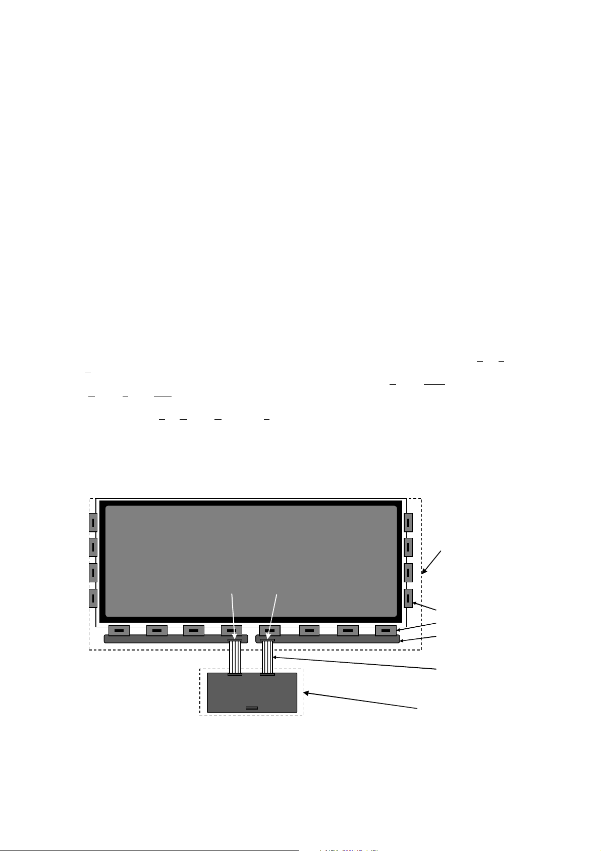
Transistor). It is composed of a color TFT-LCD panel, driver ICs, Source PWBs.
The following contents can be achieved in using LK0DZ1C0522 (Timing Control-PWB) and LK0DZ1C0383
(Control-Source-FPC) that SHARP specifies.
Graphics and texts can be displayed on a 1920 x RGB x 1080 dots panel with about seventeen million colors by
using 8bit LVDS (Low Voltage Differential Signaling) to interface, +12V of DC supply voltages.
And in order to display the moving picture smoothly, this Open Cell and C-PWB supports the Over Shoot
driving (OS driving) technology on the Single Frame Rate (SFR). In the OS driving technology, signals are
being applied to the Liquid Crystal according to a pre-fixed process as an image signal of the present frame
when a difference is found between image signal of the previous frame and that of the current frame after
comparing them.
TFT LCD Panel
(1920 x RGB x 1080)
Open Cell
K]
CN2
CN1
Gate Driver
Source Driver
Source PWB (S-
CS-FPC
CN1
1
Control PWB (C-PWB)
383
522]
Page 4
3. Mechanical Specifications
Parameter
s Specifications
Unit
80.131
(Diagonal)
cm
31.5475
(Diagonal)
inch
Active area
698.40
(H) x
382.85
(V) mm
Pixel pitch
0.3
6375
(H) x 0.
36375
(V) mm
Pixel configuration
R, G, B vertical stripe
Display mode
Normally black
O
utline d
imensions [Note1]
723.08 (H) x
444.4
(V) x
2.85 (D) mm
Mass
1.3+0.3 kg
- Front polarizer :
Super Low Haze
Anti Glare
Pin No.
Symbol
Function
Remark
Display size
LD-K25310B-2
Pixel format
Surface treatment [Note2,3]
[Note1] The thickest point is 80pin CN of S-PWB, the polarizer area thickness is shown the outline drawing in
P19.
[Note2] With the protection film removed.
[Note3] Surface resistance of the protection film adhesive side is 1010 ohm/sq.
1920 (H) x 1080 (V)
(1pixel = R + G + B dot)
Hard coating 2H and more, Haze: Less than 3%
- Rear polarizer : Hard coating less (B)
pixel
▲B-1
4. Open Cell Driving Specifications
4.1. Driving Interface of C-PWB SHARP specifies [LK0DZ1C0522]
CN1: Power and LVDS data input
Using connector: FI-RNE51SZ-HF (Japan Aviation Electronics Ind., Ltd.)
-
Mating connector: FI-RE51HL, FI-RE51CL or equivalent device (Japan Aviation Electronics Ind., Ltd.)
-
Mating LVDS transmitter: THC63LVD1023 or equivalent device
-
1 P_VCC +12V Power Supply
2 P_VCC +12V Power Supply
3 P_VCC +12V Power Supply
4 P_VCC +12V Power Supply
5 P_VCC +12V Power Supply
6 NC It is required to set non-connection (OPEN)
7 GND
8 GND
9 GND
10
11 CH1_0+ LVDS differential data input
12
13
14
15 CH1_2+ LVDS differential data input
16 GND
17
18
19 GND
20
21
22
23 Reserved
24 GND
25
26
CH1_0-
CH1_1-
CH1_1+
CH1_2-
CH1_CLKCH1_CLK+
CH1_3-
CH1_3+
Reserved
CH3_0-
CH3_0+
LVDS differential data input
LVDS differential data input
LVDS differential data input
LVDS differential data input
LVDS Clock signal
LVDS Clock signal
LVDS differential data input
LVDS differential data input
LVDS differential data input
LVDS differential data input
Page 5
27
LVDS differential data i
nput
Pin No.
Sym
bol Function
Remark
Terminal
3.3V
Terminal
ohm
CH3_1-
LVDS differential data input
28 CH3_1+ LVDS differential data input
29
30
31
32 CH3_CLK33
34
35
CH3_2-
CH3_2+
GND
CH3_CLK+
GND
CH3_3-
LVDS differential data input
LVDS differential data input
LVDS Clock signal
LVDS Clock signal
LVDS differential data input
36 CH3_3+
37
38
Reserved
Reserved
39 GND
40 SCL_I I2C CLK
41 NC
42 NC
43 WP
It is required to set non-connection (OPEN)
It is required to set non-connection (OPEN)
I2C bus enable (L/Open: disable, H: enable)
44 SDA_I I2C DATA
45 LVDS_SEL
Select LVDS data order [Note4]
Pull down: GND [Note3]
46 BIST_EN Test pattern enable (L/Open: enable, H: disable)
47 NC It is required to set non-connection (OPEN)
48 NC It is required to set non-connection (OPEN)
49 NC It is required to set non-connection (OPEN)
50 NC It is required to set non-connection (OPEN)
51 NC It is required to set non-connection (OPEN)
CN3: Aging Test Pattern Control
Using connector: 20037WR-08 (YeonHo)
-
LD-K25310B-3
Pull up: 3.3V [Note1]
[Note2]
Pull up: 3.3V [Note1]
[Note4]
1 VDD12V
2 VDD12V
+12V Power Supply
+12V Power Supply
3 GND
4 A_EN Test pattern enable (L/Open: enable, H: disable)
5 WP
I2C bus enable (L/Open: disable, H: enable)
[Note4]
[Note2]
6 SDA I2C DATA Pull up: 3.3V [Note1]
7 SCL
I2C CLK
Pull up: 3.3V [Note1]
8 GND
[Note] GND of a liquid crystal panel drive part should be connected with a module chassis.
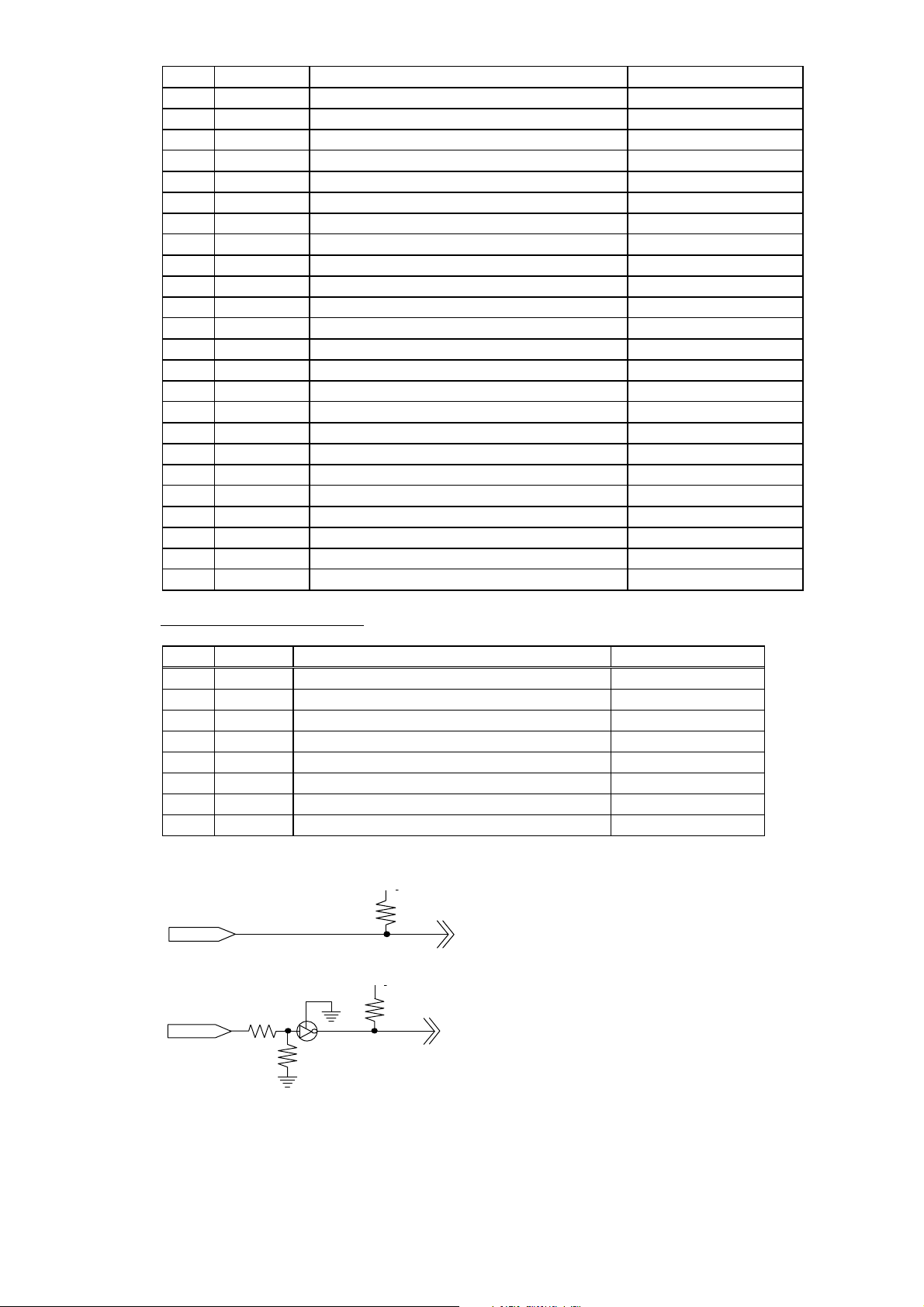
[Note1] The equivalent circuit figure of the terminal for SCL_I, SDA_I.
4.7kohm
[Note2] The equivalent circuit figure of the terminal for WP.
3.3V
4.7kohm
22
10kohm
I2C control is for EDID writing and Vcom adjustment.
Page 6
[Note3] The equivalent circuit figure of the terminal for LVDS_SEL.
Terminal
ohm
Terminal
ohm
3.3V
LVDS_SEL
Data
H(3.3V)
L(GND) or Open
TA0 R0(LSB)
R2
TA1 R1 R3
TA2 R2 R4
TA3 R3 R5
TA4 R4 R6
TA5 R5 R
7(M
SB)
TA6 G0(LSB)
G2
TB0 G1 G3
TB1 G2 G4
TB2 G3 G5
TB3 G4 G6
TB4 G5 G7(MSB)
TB5 B0(LSB)
B2
TB6 B1 B3
TC0 B2 B4
TC1 B3 B5
TC2 B4 B6
TC3 B5 B7(MSB)
TC4 NA NA
TC5 NA NA
TC6 DE(*)
DE(*)
TD0 R6 R0
TD1 R7 R1
TD2 G6 G0
TD3 G7 G1
TD4 B6 B0
TD5 B7 B1
TD6 N/A N/A
100ohm
10k
[Note4] The equivalent circuit figure of the terminal for BIST_EN, A_EN.
4.7k
LD-K25310B-4
100ohm
[Note5] LVDS Data order
[VESA]
[JEIDA]
NA: Not Available
(*)Since the display position is prescribed by the rise of DE (Display Enable) signal, please do not fix DE
signal during operation at ”High”.
Page 7
LVDS_SEL = High (3.3V) : VESA
R1R0G0
4R3R2
CH1_0
-, CH3_0
-
G2
G5G4G3G2G1
CH1_1
+, CH3_1+
-
B3B6DENANAB5B4
CH1_2
+, CH3_2+
-
+
-
R6
NAB7B6G7G6R7R6
NA
-
1
cycle
2
3
6G5G4G3
DENANA
DE
NA
0
G1G0R1R0
NA
1
cycle
CH1_0
+,
CH3_0+
CH1_0
-, CH3_0
-
CH1_1
+,
CH3_1+
CH1_1
-, CH3_1
-
CH1_2
+,
CH3_2+
CH1_2
-, CH3_2
-
CH1_CLK
+,
CH3_CLK
+
CH1_CLK
-, CH3_CLK
-
CH1_3
+,
CH3_3+
CH1_3
-, CH3_3
-
1 dot
1 pixel
CH1_CLK+, CH3_CLK
CH1_CLK-, CH3_CLK
LD-K25310B-5
CH1_0+, CH3_0+
CH1_1-, CH3_1
CH1_2-, CH3_2
CH1_3+, CH3_3+
CH1_3-, CH3_3
G1 B1 B0
R7
LVDS_SEL = Low (GND) or OPEN : JEIDA
R3 R2 G2R7 R6 R5 R4 R3 R2 G
R5 R
R1 R0 G0
B1
B3 B2 DE
G4G
B5 B4
R1 R0
B3 B2 G7G
B1 B
B5
B7 B6 B5 B4
DE: Display Enable, NA: Not Available (Fixed Low)
4.2. Vcom adjustment
For the prevention of long-time image sticking of TFT-LCD panel, be sure to adjust Vcom in such ways that
flicker is minimum on the center of display by visual or flicker meter.
- Vcom IC : MAX9684ETP+ (Maxim Integrated Products, Inc.) for I2C control from CN1 (Pin No. 40, 43,
44) or CN3 (Pin No.5,6,7) of C-PWB SHARP specifies [LK0DZ1C0522]
- Adjustment pattern :
---
V0
V128V0V128V0V128V0V128
V0
---
V128V0V128V0V128V0V128V0V128
V0
V128V0V128V0V128V0V128
1 pixel
---
V0
---
Page 8

4.3. Driving interface of S-PWB
CN1 CN2
GND
GND
Gate Power (L)
Gate Power (L)
Gate Power (H)
Gate Power (H)
Gate Start Pulse
2 Gate Start Pulse 2
Gate Start Pulse1
Gate Start Pulse 1
Gate Clock
Gate Clock
Gate Output Enable
Gate Output Enable
Gate
Scan Control
Gate Scan Control
MPD Control 1
MPD Control 1
MPD Control
2 MPD Control
2
MPD Control
3 MPD Control
3
MPD Control
4 MPD Control
4
MPD Control
5 MPD Control
5
MPD Control
6 MPD Control
6
MPD Control
7 MPD Control
7
MPD Control
8 MPD Control
8
MPD Control
9 MPD Control
9
MPD Control
10 MPD Control
10
MPD Control
11 MPD Control
11
MPD Contr
ol 12 MPD Control
12
GND
GND
GND
GND
GND
GND
GND
GND
GND
GND
GND
GND
CN1 and CN2 on the S-PWB: Input signal from C-PWB
- Using connector: 04 6806 080 000 846+ (KYOCERA Connector Products) or equivalent connector
Pin No.
1
2
3
4
5
6
7
8
9
10
11
12
13
14
15
16
17
18
19
20
21 Vcom Vcom
22 Gray Level 9 (H) Gray Level 9 (H)
23 Gray Level 8 (H) Gray Level 8 (H)
24 Gray Level 7 (H) Gray Level 7 (H)
25 Gray Level 6 (H) Gray Level 6 (H)
26 Gray Level 5 (H) Gray Level 5 (H)
27 Gray Level 4 (H) Gray Level 4 (H)
28 Gray Level 3 (H) Gray Level 3 (H)
29 Gray Level 2 (H) Gray Level 2 (H)
30 Gray Level 1 (H) Gray Level 1 (H)
31 miniLVDS data(+) GND
32 miniLVDS data(-)
33 miniLVDS data(+)
34 miniLVDS data(-)
35 miniLVDS data(+)
36 miniLVDS data(-)
37 GND
38 miniLVDS clock(+)
39 miniLVDS clock(-)
40 GND
41 miniLVDS data(+)
42 miniLVDS data(-)
43 miniLVDS data(+)
44 miniLVDS data(-) miniLVDS Cascade Control 2
45 miniLVDS data(+) miniLVDS Scan Control
46 miniLVDS data(-) miniLVDS Cascade Control 1
47 Logic Circuit Power Logic Circuit Power
48 Logic Circuit Power Logic Circuit Power
49 Reserved Reserved
50 Polarity Control Polarity Control
LD-K25310B-6
Page 9

51 Latch Strobe Latch Strobe
GND
GND
GND
GND
GND
GND
GND
GND
GND
GND
GND
GND
miniLVDS data(
-)
Analog circuit power
Analog circuit power
Analog circuit power
Analog circuit po
wer
Gray Level 1 (L)
Gray Level 1 (L)
Gray Level 2 (L)
Gray Level 2 (L)
Gray Level 3 (L)
Gray Level 3 (L)
Gray Level 4 (L)
Gray Level 4 (L)
Gray Level
5 (L) Gray Level
5 (L)
Gray Level 6 (L)
Gray Level 6 (L)
Gray Level
7 (L) Gra
y Level
7 (L)
Gray Level 8 (L)
Gray Level 8 (L)
Gray Level
9 (L) Gray Level
9 (L)
GND
GND
Parameter
Symbol
Condition
Ratings
Unit Remark
Input voltage
VI
Ta=25
o
C -
0.3 ~ 3.6
V
[Note1]
12V supply
voltage
VCC
Ta=25
o
C 0 ~ +14
V
LVDS Voltage
VLVDS
Ta=25
o
C -
0.3 ~ 3
V
[Note2]
Operation temperature
Topa
-
0 ~ +60
oC [Note3]
52 GND GND
53 miniLVDS Cascade Control 2 miniLVDS data(+)
54 miniLVDS Scan Control miniLVDS data(-)
55 miniLVDS Cascade Control 1 miniLVDS data(+)
56 GND miniLVDS data(-)
57
58
59
60
61
62
63
64
65
66
67
68
69
70
71
72
73
74
75
76
77
78
79
80
miniLVDS data(+)
miniLVDS data(-)
GND
miniLVDS clock(+)
miniLVDS clock(-)
GND
miniLVDS data(+)
miniLVDS data(-)
miniLVDS data(+)
miniLVDS data(-)
miniLVDS data(+)
4.4. Electrical characteristics of input voltage
LD-K25310B-7
[Note1] LVDS_SEL, I2C_SCL, I2C_SDA, WP
[Note2] CH1_CLK±, CH1_0±, CH1_1±, CH1_2±, CH1_3±,
[Note3]
-
-
-
-
-
Storage temperature Tstg - -25 ~ +60
o
C [Note3]
CH3_CLK±, CH3_0±, CH3_1±, CH3_2±, CH3_3±
Humidity: 95%RH Max.(Ta < 40oC)
Maximum wet-bulb temperature at 39oC or less. (Ta > 40oC)
No condensation.
Be sure to design the module with maintaining temperature of the panel at 60oC or less and uniform as much
as possible. Otherwise there is possibility to cause several issue such as Mura or Gamma shift, etc.
Be sure to follow the each part’s recommended conditions of use about the part of producing heat itself, driver IC.
Page 10

4.5. Electrical characteristics of input signals
Parameter
Symbol
Min. Typ. Max.
Unit Remark
Supply voltage
Vcc 11.4 12.0 12.6 V [Note1]
Current dissipation
Icc - 0.8 2.9 A [Note2]
t1=500us
Permissible input ripple voltage
VRP - -
100 mV
Vcc = +12.0V
Input Low voltage
VIL 0 -
0.7 V
Input High voltage
VIH
2.3 - 3.3 V
VI = 3.3V
Terminal resistor
RT -
100 - ohm Diff
erential input
Input Differential voltage
|VID|
200 400 600 mV [Note4]
Differential input
V1
=10.8V
V2
=9.1V
ON
t4
0.9 Vcc
0.1V cc
OF F
ON
Data1
t2
ON
0.9 Vcc
0.1V cc
0.1V cc
ON
LD-K25310B-8
Ta=25oC
+12V supply voltage
Inrush current
I
RUSH
I
RUSH
Input leak current (High) I
common mode voltage
VCM |VID|/2 1.2 2.4-|VID|/2 V [Note4]
[Note] VCM: Common mode voltage of LVDS driver.
[Note1]
Input voltage sequences
50us < t1 < 20ms
20ms < t2 < 5s
20ms < t3 < 5s
0 < t4 < 1s
700ms < t5-1
700ms < t5-2
▲B-2
▲B-2
0 < t6 -1
0 < t6 -2
1s < t7
Vcc
t1
t7
t3
Data2
t5-2
Back li ght:V
t5-1
t3
t6-2
-1
OFF
※ Data1: CH1_CLK±, CH1_0±, CH1_1±, CH1_2±, CH1_3±
CH3_CLK±, CH3_0±, CH3_1±, CH3_2±, CH3_3±
*VCM voltage pursues the sequence mentioned above.
※ Data2: LVDS_SEL, SCL_I, SDA_I, WP
[Note] About the relation between data input and back light lighting, please base on the above-mentioned
input sequence. When back light is switched on before panel operation or after a panel operation
stop, it may not display normally. But this phenomenon is not based on change of an incoming
signal, and does not give damage to a liquid crystal display.
1
- 2.5 - A
2
- 1.2 - A t1>5ms
IH1
- - 400 µA
Dip conditions for supply voltage
a) V2 < Vcc < V1
td < 10ms
b) Vcc < V2
This case is based on input voltage sequences.
td
[Note5]
P-P
[Note3]
[Note3]
Vcc
Page 11

R G B
G S 0
R G B
G S 1
R G B
R G B
R G B
G S
2 5 5
CH*_CL
K+,
VCM
|VID|
|VID|
GND
CH*_
CLK-,
I
RUSH
1
t1
Vcc
Icc
[Note2] Typical current situation: 255 gray-bar patterns. (Vcc = +12.0V)
The explanation of RGB gray scale is seen in section 4.8.
G S 2
. ...
G S 2 5 4
Vcc = +12.0V
1/Tc = 74.25MHz
TH = 14.8µs
TV = 60Hz
[Note3] LVDS_SEL, WP
[Note4] CH1_CLK±, CH1_0±, CH1_1±, CH1_2±, CH1_3±,
CH3_CLK±, CH3_0±, CH3_1±, CH3_2±, CH3_3±
CH*_Data-
CH*_Data+
[Note5] Vcc12V inrush current waveform
LD-K25310B-9
Page 12

4.6. Timing characteristics of input signals
Clock
Frequency
1/Tc 69.0 74.25
76.0 MHz
1050
1100
1300
clock
14.2 14.8 16.1 µs
Horizontal period
1109
1125
1400
line
47 60 63 Hz
Vertical period
19
20
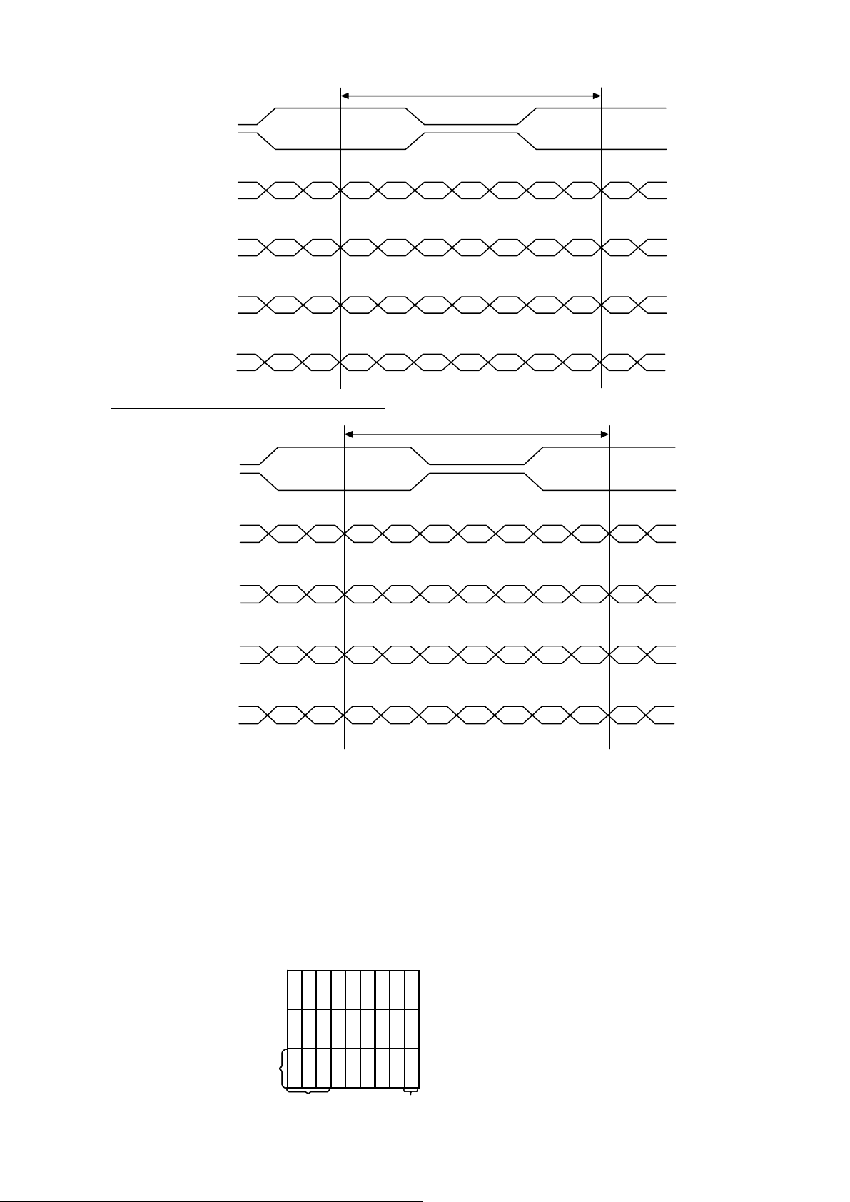
Timing diagrams of input signal are shown in below figure.
Parameter Symbol Min. Typ. Max. Unit Remark
Horizontal period TH
LD-K25310B-10
Data
Enable
Signal
(High)
THd
Vertical period TV
(High)
TVd 1080 1080 1080 line
960
960
960
clock
[Note]
-
When vertical period is very long, flicker and etc. may occur.
-
Please turn off the module after it shows the black screen.
-
Please make sure that length of vertical period should become of an integral multiple of horizontal length
of period. Otherwise, the screen may not display properly.
-
As for your final setting of driving timing, we will conduct operation check test at our side, please inform
your final setting.
TH
THd
DE
CH1 Data
(R G, B)
19
1 3
1917
1919
CH3 Data
(R, G, B)
DE
19
Tc
2 4
TV
Timing diagram of input signal
1918
1 2 1079 1080
1920
TVd
Page 13

4.7. Input data signal and display position on the screen
SHARP
-
-
Item Symbol
Min. Typ. Max.
Unit
Delay time, CLK rising edge
Delay time, CLK rising edge
Delay time, CLK risi
ng edge
Delay time, CLK rising edge
Delay time, CLK rising edge
Delay time, CLK rising edge
Delay time, CLK rising edge
R1 G1 B1 R2 G2 B2
(1,1) (1,2)
R3 G3 B3 R4 G4 B4
(1、3) (1,4)
LD-K25310B-11
S-PWB
1,1 1,2 1,3
2,1 2,2
3,1
1080,1
1,4
S-PWB
[Note] Scan direction is setting for using S-PWBs’ side up. If you use S-PWB’s side down, please invert
the input of image.
4.8. Input data signal and display position on the screen
t
CLK
CLK
Vdiff=0V
CLK+
Data*
Data*+
tpd0
tpd1
tpd2
tpd3
tpd4
tpd5
tpd6
1,1920
1080 ,1920
Vdiff=0V
tpd0 -0.25 0 0.25
tpd1
tpd2
tpd3
tpd4
tpd5
tpd6
1*
2*
3*
4*
5*
6*
t
t
t
t
t
t
CLK
CLK
CLK
CLK
CLK
/7-0.25 1*
/7-0.25 2*
/7-0.25 3*
/7-0.25 4*
/7-0.25 5*
7-0.25 6*
CLK
t
t
t
t
t
t
CLK
CLK
CLK
CLK
CLK
CLK
/7 1*
/7 2*
/7 3*
/7 4*
/7 5*
/7 6*
t
t
t
t
t
t
CLK
CLK
CLK
CLK
CLK
CLK
/7+0.25
/7+0.25
/7+0.25
/7+0.25
/7+0.25
/7+0.25
ns
Data
position
to serial bit position 0
to serial bit position 1
to serial bit position 2
to serial bit position 3
to serial bit position 4
to serial bit position 5
to serial bit position 6
Page 14

4.9. Input signal, basic display colors and gray scale of each color
R1R2R3
R4R5R6
R7- - G0G1G2G3G4G5G6G7- -
B0
B3B4B5B6B7- -
- - - - - -
- - - - - -
- - - - - -
- - - - - -
- - - - - -
- - - - - -
Colors & Gray Scale
Basic Color Black – 0 0 0 0 0 0 0 0 - - 0 0 0 0 0 0 0 0 - - 0 0 0 0 0 0 0 0 - Blue – 0 0 0 0 0 0 0 0 - - 0 0 0 0 0 0 0 0 - - 1 1 1 1 1 1 1 1 - Green – 0 0 0 0 0 0 0 0 - - 1 1 1 1 1 1 1 1 - - 0 0 0 0 0 0 0 0 - Cyan – 0 0 0 0 0 0 0 0 - - 1 1 1 1 1 1 1 1 - - 1 1 1 1 1 1 1 1 - Red – 1 1 1 1 1 1 1 1 - - 0 0 0 0 0 0 0 0 - - 0 0 0 0 0 0 0 0 - Magenta – 1 1 1 1 1 1 1 1 - - 0 0 0 0 0 0 0 0 - - 1 1 1 1 1 1 1 1 - Yellow – 1 1 1 1 1 1 1 1 - - 1 1 1 1 1 1 1 1 - - 0 0 0 0 0 0 0 0 - White – 1 1 1 1 1 1 1 1 - - 1 1 1 1 1 1 1 1 - - 1 1 1 1 1 1 1 1 - Gray Scale of Red Black GS0 0 0 0 0 0 0 0 0 - - 0 0 0 0 0 0 0 0 - - 0 0 0 0 0 0 0 0 - -
--- GS1 1 0 0 0 0 0 0 0 - - 0 0 0 0 0 0 0 0 - - 0 0 0 0 0 0 0 0 - -
--- GS2 0 1 0 0 0 0 0 0 - - 0 0 0 0 0 0 0 0 - - 0 0 0 0 0 0 0 0 - -
--- ---
--- ---
--- GS253 1 0 1 1 1 1 1 1 - - 0 0 0 0 0 0 0 0 - - 0 0 0 0 0 0 0 0 - -
--- GS254 0 1 1 1 1 1 1 1 - - 0 0 0 0 0 0 0 0 - - 0 0 0 0 0 0 0 0 - Red GS255 1 1 1 1 1 1 1 1 - - 0 0 0 0 0 0 0 0 - - 0 0 0 0 0 0 0 0 - Gray Scale of Green Black GS0 0 0 0 0 0 0 0 0 - - 0 0 0 0 0 0 0 0 - - 0 0 0 0 0 0 0 0 - -
--- GS1 0 0 0 0 0 0 0 0 - - 1 0 0 0 0 0 0 0 - - 0 0 0 0 0 0 0 0 - -
--- GS2 0 0 0 0 0 0 0 0 - - 0 1 0 0 0 0 0 0 - - 0 0 0 0 0 0 0 0 - -
--- ---
--- ---
--- GS253 0 0 0 0 0 0 0 0 - - 1 0 1 1 1 1 1 1 - - 0 0 0 0 0 0 0 0 - -
--- GS254 0 0 0 0 0 0 0 0 - - 0 1 1 1 1 1 1 1 - - 0 0 0 0 0 0 0 0 - Green GS255 0 0 0 0 0 0 0 0 - - 1 1 1 1 1 1 1 1 - - 0 0 0 0 0 0 0 0 - Gray Scale of Blue Black GS0 0 0 0 0 0 0 0 0 - - 0 0 0 0 0 0 0 0 - - 0 0 0 0 0 0 0 0 - -
--- GS1 0 0 0 0 0 0 0 0 - - 0 0 0 0 0 0 0 0 - - 1 0 0 0 0 0 0 0 - -
--- GS2 0 0 0 0 0 0 0 0 - - 0 0 0 0 0 0 0 0 - - 0 1 0 0 0 0 0 0 - -
--- ---
--- ---
--- GS253 0 0 0 0 0 0 0 0 - - 0 0 0 0 0 0 0 0 - - 1 0 1 1 1 1 1 1 - -
--- GS254 0 0 0 0 0 0 0 0 - - 0 0 0 0 0 0 0 0 - - 0 1 1 1 1 1 1 1 - Blue GS255 0 0 0 0 0 0 0 0 - - 0 0 0 0 0 0 0 0 - - 1 1 1 1 1 1 1 1 - -
-
0: Low level voltage / 1: High level voltage
-
Each basic color can be displayed in 256 gray scales from 8 bits data signals. According to the
combination of total 24 bits data signals, about 17 million-color display can be achieved on the screen.
Data signal
LD-K25310B-12
B1B2
Page 15

5. Optical Characteristics
Parameter
Symbol
Condition
Min. Typ. Max.
Unit Remark
Response time
τ
- 7 - ms [Note3,4,5]
x Typ-0.03 (
0.2
80) Typ+0.03
-
y Typ-0.03 (0.290)
Typ+0.03
-
x Typ-0.03 (0.645)
Typ+0.03
-
y Typ-0.03 (0.330)
Typ+0.
03 -
x Typ-0.03 (0.290)
Typ+0.03
-
y Typ-0.03 (0.615)
Typ+0.03
-
x Typ-0.03 (0.145)
Typ+0.03
-
y Typ-0.03 (0.055)
Typ+0.03
-
x Typ-0.03 (Wx)
Typ+0.03
-
y Typ-0.03 (Wy)
Typ+0.03
-
Luminance
White
YL - (350) -
cd/m
2
[Note4
,7]
Luminance uniformity
White
δ
- - (1.34)
-
[Note6]
Gamma
γ
Typ-0.35 (2.2) Typ+0.35
-
[Note4,7,9]
urement of Contrast, Luminance, Chromaticity.
Horizontal
Viewing
angle range
Vertical
Contrast ratio CRn
White
Red
Chromaticity
Green
Blue
LD-K25310B-13
Ta=25oC, Vcc=12.0V, Timing=60Hz (typ. value)
21
θ
θ
θ
θ
22
11
12
DRV
CR>10
=0 deg.
θ
70 88 - Deg.
70 88 - Deg.
- 4000
- - [Note2,4]
[Note1,4]
[Note4,7]
ACC
[Note4,7,8]
w
- Optical characteristics (except Note7) are based on SHARP standard LED module’s backlight system.
- Measurement condition: Set the maximum luminance of LED.
- The measurement shall be executed 60 minutes after lighting at rating.
[Note] The optical characteristics are measured using the following equipment.
Detector (EZ-CONTRAST/Photodiode)
Middle of the screen (θ=0°)
TFT-LCD Module
Measurement of viewing angle range and Response time.
-Viewing angle range: EZ-CONTRAST
- Response time: Photodiode
400mm
Middle of the screen (θ=0°)
TFT-LCD Module
Meas
Detector (SR-3A-L1)
Field=1°
[Note1] Definitions of the viewing angle range:
θ
θ
12
22
Normal line
θ
θ
11
21
6 o’clock direction
Page 16

[Note2] Definition of the contrast ratio:
Gray level of End (y)
0%
25% 50% 75% 100%
0%
tr: 0%
-
25% tr: 0%
-
50% tr: 0%
-
75% tr: 0%
-
100%
25% td: 25%
-0% tr: 25%
-
50% tr: 25%
-
75% tr: 25%
-
100%
50% td: 50%
-0%
td: 50%
-
25%
tr: 50%
-
75% tr: 50%
-
100%
75% td: 75%
-0%
td: 75%
-
25% td: 75%
-
50%
tr: 75%
-
100%
100%
td: 100%
-0%
td: 100%
-
25% td: 100%
-
50% td: 100%
-
75%
Time
Bright
Bright
0
9601600
180
540
900
I
B
The contrast ratio is defined as the following.
=RatioContrast
[Note3] Definition of the response time
The response time (
) is defined as the following.
τ
rd
rd
+=τ
∑∑
is the average value of the switching time from five gray levels (0%, 25%, 50%, 75% and 100%) to five
τ
rd
gray levels (0%, 25%, 50%, 75% and 100%).
Start (x)
Gray level of
100%
90%
20y)}-x:td(y)-x:tr({
Dark
LD-K25310B-14
whitepixels all with s)(brightnes Luminance
black pixels all with s)(brightnes Luminance
10%
0%
Photo detector Output (Relative Value)
τ
d
τ
r
[Note 4] This value shall be measured at center of the active area.
[Note 5] This value is valid when O/S driving is used at typical input time value.
[Note 6] Definition of the white uniformity;
White uniformity is defined as the following with nine measurements. (A∼I)
w =δ
E"" pointscenter of Luminance
32
A
C
D
E
F
G
H
[pixels]
E""point center of Luminance - points nine of luminance Minimumor Maximum
[Note7] These values are for reference based on measurement result by SEC backlight system and measurement
[Note8] Definition range of ACC is V32/255~V248/255.
[Note9] Definition range of Gamma is V50/255~V200/255.
conditions.
Page 17

6. Packing for Shipping
1 palette
1 box
Size 1200
x 1
000 x 1003
(H) [mm]
831 x 558.5
x 129(H) [mm]
Q’ty 238 open cells
17
open cells
Mass
Max. 33
0 kg Max. 22
kg
Lot No.
[Note1]
No.
[Note1]
month (1~9,X,Y,Z)
HARP Management Area
38
3838
38
Qu anti t y
pc s
Lo tNo.
Z1 2 345
社内 品 番
Bar co de
Bar cod e
Bar code
LK3 1 5D 3H A9 K
17
2 013.
0 4.01
. 12 345
Bar code
6.1. Packing Form
- Please refer to the attached drawing for details. (P20)
- Don’t guarantee other than shipment by the palette.
6.2. Label
a) Open Cell label
This label is pasted on the S-PWB. Please refer to the attached drawing for the pasting area. (P19)
ex) LK315D3HA9K
LD-K25310B-15
Model No.
How to express Lot No.
O O O O O O O O O O O
S
Suffix code
Production code
Production
Production year (the last figures of the Christian Era)
Sequence
Serial No.
b) Packing labels
These labels are stuck on the cell box and palette.
Cell Box Labe l
ex) LK 31 5D3H A9K
⑤ S HARP Logisti cs Manage ment Area
:
(((( 4444S ) L K
S) L K315D 3 HA 9 K
315D 3 HA9 K
S) L KS) L K
315D 3 HA9 K3 1 5D 3 HA9K
:(1T ) 201 3.04 . 01
:(Q)
ユー ザー品番
社外品番 :
社内品番 :
員数 : 梱包 MK :
LotN O.2 :
① Mode l No.& Suffix Code
② Lot No.
③ Quant ity
④ Use r Code ▲B-3
: BN9 6 -28 47 7 A
Ba rc ode
LK3 1 5D 3H A9 K
17
Palette Label
ex) LK 31 5D3HA9K
①
②
③
④
⑤
Barcode (Serial No.)
[Note1] Production Code & Suffix Code
Plant Model No. Production
Code
Japan LK315D3HA9K
L (non)
KAM EYAM A P L ANT NO. 2
KAM EYAM A P L ANT NO. 2
KAM EYAM A P L ANT NO. 2K AM E YAM A P L ANT NO. 2
2222
LK 315D3 H A9
LK 315D3 H A9 KKKK
LK 315D3 H A9LK 315D3 H A9
20 13 04 0 1 ( 2 0 130 4
20 13 04 0 1 ( 2 0 130 4 01
20 13 04 0 1 ( 2 0 130 420 13 04 0 1 ( 2 0 130 4
23 8
23 8
23 823 8
BN9 6
BN9 6----28 47 7A
28 47 7A
BN9 6BN9 6
28 47 7A28 477A
LK3 15D 3 H A9K
LK3 15D 3 H A9K
LK3 15D 3 H A9KLK3 15D 3 H A9K
[N ote1] This code may differ from “Model No. & Suf fix”.
01 ))))
0101
Suffix Code
① SH ARP Logosti cs
①
Mana gement Ar ea
② SH ARP War ehou sin g Code
[Note 1]
③ P acking D ate
④ O pen Cell Q uantity
②
⑤ U ser Code ▲ B-3
③
④
⑤
①
Page 18

7. Reliability Test Item
No. Test item (Test sample form)
Condition
High temperature storage test
70oC, 500h
Low temperature storage test
-
35oC, 500h
High temperature and
50oC, 95%RH, 500hr
High temperature operation test
60oC, 500h
High temperature
60oC with window pattern ( 5 x 3 cm )
Low temperature operation test
-
10oC, 500h
Turn on after
After left at low temperature (
-
10oC) for 24hr or more, operation checking
8 Heat cycle test
(Open Cell)
-35oC, 30min <
----
> 70oC, 30min, 100cycle
Press reduction storage test
15,000ft,
-
20oC, 10hr
ESD
test (Open Cell)
Input
up to
+
15kV
10times from
every
terminal
of CN1 and CN2 with
Power ON/OFF test
-
10oC and 60
o
C, ON/OFF time :
10sec, 1,000cycle
Polarizer moisture absorption test
0oC, 1hr <
---
> 30oC, 95%RH, 1hr, 10cycle
Flushing test
140mm or less flushing area by applying pressure at 19.6N/cm
2
after
Vibration test
X and Y direction: 15min, Z direction: 60min.
Drop test
Height: 15cm (1 face and 2 sides)
Pad corrosion test
50oC, 95%RH, 1,000hr
LD-K25310B-16
10
1
2
3
high humidity operation test
(Open Cell)
(Open Cell)
(No condensation)
(Open Cell)
4
(Open Cell)
(With checking Vgl margin variability)
(With checking driving part (driver, PCB) temperature by radiation
thermometer.)
5
6
image sticking test
(Open Cell)
(Open Cell)
12hr / 72hr / 168hr / 336hr
Window pattern is invisible at 60% gray level.
(After leaving for 5hr at -10oC, operating at normal condition for 1hr, then
operation checking at normal condition.)
7
low temperature storage
at normal condition.
(Open Cell)
9
(Open Cell)
non-operation ▲A
11
12
13
(Open Cell)
(Open Cell)
for liquid crystal amount
operating at 60oC for 1hr.
(Open Cell)
14
(1 Cell Box with full Open Cells)
15
(1 palette with full Open Cells)
16
(Open Cell in cell box)
5Hz to 50Hz acceleration velocity: 1.0G, Sweeping ratio: 3min
Number: 3 times (1 time in each of drop direction)
[Result evaluation criteria]
Under the display quality test condition with normal operation state, there shall be no change (except No.5), which
may affect practical display function.
8. Precautions
a) Be sure to turn off the power supply when inserting or disconnecting the cable.
b) Be sure to design the cabinet so that the Open Cell can be installed without any extra stress such as warp or twist.
c) Since the polarizer is easily damaged, pay attention not to scratch it.
d) Since long contact with water may cause discoloration or spots, wipe off water drop immediately.
e) When the polarizer is soiled, wipe it with absorbent cotton or other soft cloth.
f) Since the panel is made of glass, it may break or crack if dropped or bumped on hard surface. Handle with care.
g) The Open Cell has some PWBs, take care to keep them from any stress or pressure when handling or installing the
Open Cell, otherwise some of electronic parts on the PWBs may be damaged.
h) When handling the Open Cell and assembling them into cabinets, please be noted that long-term storage in the
environment of oxidization or deoxidization gas and the use of such materials as reagent, solvent, adhesive, resin, etc.
which generate these gasses, may cause corrosion and discoloration of the Open Cell.
i) Applying too much force and stress to PWB and SOF may cause a malfunction electrically and mechanically.
j) The Open Cell has high frequency circuits. Sufficient suppression to EMI should be done by system manufacturers.
k) The chemical compound, which causes the destruction of ozone layer, is not being used.
Page 19

l) Precautions of peeling off the protection film.
Item Management standard value and performance standard
1 Anti-static mat (shelf)
1 to 50 [M ohm]
2 Anti-static mat (floor, desk)
1 to 100 [M ohm]
3 Ionizer
Attenuate from
+
1000V to
+
100V within
2 sec
4 Anti-static wrist band
0.8 to 10 [M ohm]
5 Anti-static wrist band entry and
Below 1000 [ohm]
6 Temperature
22 to 26 [
o
C]
7 Humidity
60 t
o 70 [%]
X
O
LD-K25310B-17
m) Since the Open Cell consists of TFT and electronic circuits with CMOS-ICs, which are very weak to electrostatic
discharges, persons who are handling the Open Cell should be grounded through adequate methods such as the
anti-static wrist band. Connector pins should not be touched directly with bare hands.
- Reference : Process control standard of sharp
ground resistance
- Be sure to peel off slowly (recommended more than 5sec) and
constant speed.
- Peeling direction shows Fig.
- Be sure to ground person with adequate methods such as the
anti-static wrist band.
- Be sure to ground all terminals of the S-PWB while peeling of
the protection film.
- Ionized air should be blown over during peeling action.
- The protection film must not touch drivers and S-PWBs.
- If adhesive may remain on the polarizer after the protection film
peeling off, please remove with isopropyl-alcohol.
n) Do with the actuator opened completely, and insert it in the interior of the insertion entrance surely horizontally
when you insert FPC. (Please put the FPC tab in the ditch of the housing surely with the FPC tab.) Might it become
short defective, and it causes the corner to transform the caught terminal into the terminal by the pitch gap when
inserting it right and left and diagonally.
o) Please add force in the direction where the actuator is held and do by rotating it pushing in parallel to the S-PWB
direction when becoming 90o or less as shown in the figure below until the angle of the actuator becomes 90o or less
when you shut the actuator. Please do not add the force to rotary axis of actuator in the direction that the actuator is
off.
p) When you lock, it should be push on both sides of the actuator. And it is necessary to confirm that the actuator is
surely shut.
q) Please be careful since image retention may occur when a fixed pattern is displayed for a long time.
r) This Open Cell is corresponded to RoHS. ‘‘R.C.’’ label on the side of palette shows it.
s) When any question or issue occurs, it shall be solved by mutual discussion.
Page 20

9. Storage Conditions of Open Cell in Cell Box
- Temperature
0oC to 40
o
C
- Humidity
95% RH or less
- Reference condition
20oC to 35
o
C, 85% RH or less (summer)
- Sunlight
Be sure to shelter a production from the direct sunlight.
- Atmosphere
Harmful gas, such as acid and alkali which bites electronic components and/or wires
- Notes
Be sure to put cartons on pale
tte or base, don’t put it on floor, and store them with
- Storage life
1 year.
5oC to 15oC, 85% RH or less (winter)
The total storage time (40oC, 95% RH) : 240h or less
must not be detected.
removing from wall.
Please take care of ventilation in storehouse and around cartons, and control changing
temperature is within limits of natural environment.
LD-K25310B-18
Page 21

LD-K25310B-19
Outline Drawing of Open Cell [LK315D3HA9K]
Page 22

LD-K25310B-20
Cell Box(Top)
32inch Open Cell
: 17pcs
Panel Protective Pad
: 18pcs
Spacer
Cell Box (Bottom)
ex)
Cell Box Label
ex)Palette
Label
ing Unit
Top Sheet
Bottom Sheet
Palette
Side Frame &
PP Band
PP Band
[Surface resistance : 10
[Expansion Ratio : x30]
9~11
ohm/sq
▲B-4
]
[Surface resistance : 109ohm/sq]
Stretch Film (Double Winding)
[Surface resistance : 10
[Expansion Ratio : x30]
9~11
ohm/sq
▲B-4
1 Palette (2 x 7 boxes)
1 Cell Box
]
Drawing of Pack
 Loading...