


®
PRODUCT SPECIFICATIONS
Integrated Circuits Group
LH28F320BJE-PTTL90
Flash Memory
32M (2M × 16/4M × 8)
(Model No.: LHF32J02)
Spec No.: EL124011
Issue Date: April 17, 2000
SHARP
LHF32JO2
l Handle this document carefully for it contains material protected by international copyright law.
Any reproduction, full or in part, of this material is prohibited without the express written
permission of the company.
l When using the products covered herein, please observe the conditions written herein and the
. precautions outlined in the following paragraphs. In no event shall the company be liable for any
damages resulting from failure to strictly adhere to these conditions and precautions.
(1) The products covered herein are designed and manufactured for the following application
areas. When using the products covered herein for the equipment listed in Paragraph (2),
even for the following application areas, be sure to observe the precautions given in
Paragraph (2). Never use the products for the equipment listed in Paragraph (3).
*Office electronics . t
l Instrumentation and measuring equipment
*Machine tools
*Audiovisual equipment
*Home appliance
@Communication equipment other than for trunk lines
--
(2) Those contemplating using the products covered herein for the following equipment which
demands high reliability, should first contact a sales representative of the company and then
accept responsibility for incorporating into the design fail-safe operation, redundancy, and
other appropriate measures for ensuring reliability and safety of the equipment and the
overall system.
*Control and safety devices for airplanes, trains, automobiles, and other
transportation equipment
*Mainframe computers
*Traffic control systems
l Gas leak detectors and automatic cutoff devices
*Rescue and security equipment
*Other safety devices and safety equipment, etc.
(3) Do not use the products covered herein for the following equipment which demands
extremely high performance in terms of functionality, reliability, or accuracy.
*Aerospace equipment
l Communications equipment for trunk lines
*Control equipment for the nuclear power industry
*Medical equipment related to life support, etc.
(4) Please direct all queries and comments regarding the interpretation of the above three
Paragraphs to a sales representative of the company.
l Please direct all queries regarding the products covered herein to a sales representative of the
company.
Rev. 1.26
SHARI=
LHF32JO2 1
CONTENTS
PAGE PAGE
1 INTRODUCTION.. ............................................................ 3 5 DESIGN
1.1 Features ........................................................................ 3 5.1 Three-Line Output Control ........................................ 27
1.2 Product Overview.. ......................................................
1.3 Product Description.. ....................................................
1.3.1 Package Pinout .: .......................... . ..... ..- .... . ..............
1.3.2 Block Organization ................................................ .4
2 PRINCIPLES OF OPERATION.. ..................................... .8
2.1 Data Protection.. .......................................................... .8 5.8 Data Protection
3 BUS OPERATION ........................................................... .9
3.1 Read .............................................................................. 9
3.2 Output Disable.. ........................................................... .9
3.3 Standby
3.4 Reset ............................................................................. 9
3.5 Read Identifier Codes.. ............................................... 10
3.6 OTP(One Time Program) Block.. .............................. 10
3.7 Write.. ......................................................................... 11
1 COMMAND DEFINITIONS.. ......................................... 11
4.1 Read Array Command.. .............................................. 13
4.2 Read Identifier Codes Command
4.3 Read Status Register Command.. ............................... 13
4.4 Clear Status Register Command.. ............................... 13
4.5 Block Erase Command.. ............................................. 14
4.6 Full Chip Erase Command..
4.7 Word/Byte
4.8 Block Erase Suspend Command ................................ 15
4.9 Word/Byte Write Suspend Command.. ....................... 15
4.10 Set Block and Permanent Lock-Bit Command.. ....... 16
4.11 Clear Block Lock-Bits Co mmand.. .......................... 16
4.12 OTP Program Command .......................................... 17
4.13 Block Locking by the WP# ...................................... 17
......................................................................... 9
............................... 13
....................................... 14
Write Command.. ..................................... 14
.3 5.2 RY/BY# and WSIM Polling ....................................... 27
4 5.3 Power Supply Decoupling ......................................... 27
4 5.4 V,, Trace on Printed Circuit Boards ..................... 27
5.5 V,, . V,,,, RP# Transitions .................................... 27
5.6 Power-Up/Down Protection.. ..................................... 28
5.7 Power Dissipation ...................................................... 28
6 ELECTRICAL SPECIFICATIONS ................................ 29
6.1 Absolute Maximum Ratings
6.2 Operating Conditions.. ............................................... 29
6.2.1 Capacitance.. ........................................................ 29
6.2.2 AC
6.2.3
6.2.4 AC Characteristics - Read-Only Operations.. ...... 33
6.2.5 AC Characteristics - Write Operations
6.2.6 Alternative CE#-Controlled Writes.. .................... 38
6.2.7
6.2.8 Block Erase, Full Chip Erase, Word/Byte Write and
7 PACKAGE AND PACKING SPECIFICATIONS . . . . . . . . . . 42
CONSIDERATIONS ....................................... 27
Method.. ........................................... 28
...................................... 29
Input/Output Test Conditions ........................ 30
DC Characteristics.. ............................................. 31
................ 36
Reset Operations .................................................. 40
Lock-Bit Configuration Performance ................. 41
Rev. 1.26
SHAI?P
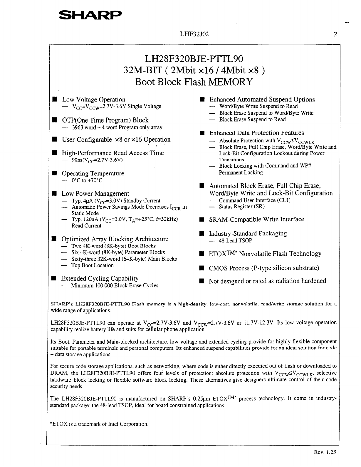
LH28F320BJE-PTTL90
32M-BIT
( 2Mbit x16 / 4Mbit
Boot Block Flash MEMORY
I Low Voltage Operation
- v
I OTP(One Time Program) Block
- 3963 word + 4 word Program only array
I User-Configurable x8 or x 16 Operation
I High-Performance Read Access Time
- 90ns(Vcc=2.7V-3.6V)
I Operating Temperature
- 0°C to +7O”C
I Low Power Management
- Typ. 4pA (Vcc=3.0V) Standby Current
- Automatic Power Savings Mode Decreases I,-, in
- Typ. 12OpA (Vc,=3.0V, TA=+25”C, f=32kHz)
Read Current
I Optimized Array Blocking Architecture
- Two 4K-word (8K-byte) Boot Blocks
- Six 4K-word @K-byte) Parameter Blocks
- Sixty-three 32K-word (64K-byte) Main Blocks
- Top Boot Location
,,=2.7V-3.6V Single Voltage
cc
=v
Static Mode
LHF32JO2
n Enhanced Automated Suspend Options
I Enhanced Data Protection Features
n Automated Block Erase, Full Chip Erase,
n
H Industry-Standard Packaging
n ETOXTM* Nonvolatile Flash Technology
n CMOS Process (P-type silicon substrate)
x8
)
- Word/Byte Write Suspend to Read
Block Erase Suspend to Word/Byte Write
-
- Block Erase Suspend to Read
- Absolute Protection with VccwSVcm,
-
Block Erase, Full Chip Erase, Word/Byte Write and
Lock-Bit Configuration Lockout during Power
Transitions
- Block Locking with Command and WP#
- Permanent Locking
Word/Byte
- Command User Interface (CUI)
- Status Register (SR)
SRAM-Compatible Write Interface
- 4%Lead TSOP
Write and Lock-Bit Configuration
2
I Extended Cycling Capability
- Minimum 100,000 Block Erase Cycles
IHARP’s LH28F320BJE-P’TTL90 Flash memory is a high-density, low-cost, nonvolatile. read/write storage solution for a
vide range of applications.
,H28F320BJE-PTTL90 can operate at V,,=2.7V-3.6V and V,,,apability realize battery life and suits for cellular phone application.
is Boot, Parameter and Main-blocked architecture, low voltage and extended cycling provide for highly flexible component
uitable for portable terminals and personal computers. Its enhanced suspend capabilities provide for an ideal solution for code
data storage applications.
‘or secure code storage applications, such as networking, where code is either directly executed out of flash or downloaded to
)RAM, the LH28F320BJE-PTTL90 offers foui levels of protection: absolute protection with VCCW<VCCWLfi selective
ardware block locking or flexible software block locking. These alternatives give designers ultimate control of their code
:curity needs.
he LH28F320BJE-PITL90 is manufactured on SHARP‘s 0.25pm ETOXT”*
:andard package: the 4%lead TSOP, ideal for board constrained applications.
ETOX is a trademark of Intel Corporation
n Not designed or rated as radiation hardened
-2.lV-3.6V or 11.7V-12.3V. Its low voltage operation
process technology. It come in industry-
Rev. 1.25
SHAR!=
--
LJSF32JO2
1 INTRODUCTION
This
specifications. Section 1 provides a flash memory
overview. Sections 2, 3, 4 and 5 describe the memory
organization and functionality. Section 6 covers electrical
specifications.
datasheet contains LH28F320BJE-PI-l-L90
1.1 Features
Key enhancements of LH28F320BJE-PTTL90 boot block
Flash memory are:
*Single low voltage operation
*Low power consumption
*Enhanced Suspend Capabilities
*Boot Block Architecture
Please note following:
l
VCCvtK has been lowered to l.OV to support 2.7V-
3.6V block erase, full chip erase, word/byte write and
lock-bit configuration operations. The V,, voltage
transitions to GND is recommended for designs that
switch V,,, off during read operation.
1.2 Product Overview
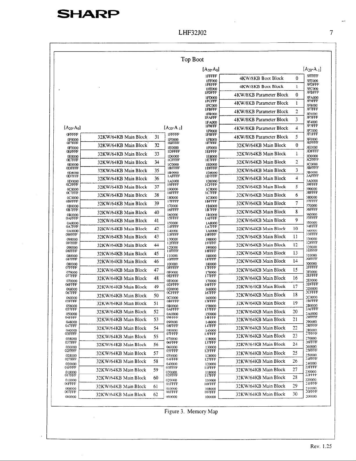
The LH28F320BJE-PTTL90 is a high-performance 32MIit Boot Block Flash memory organized as 2M-word of 16
)its or 4M-byte of 8 bits. The 2M-word/4M-byte of data is
u-ranged in two 4K-word/8K-byte boot blocks, six 4Kvord/8K-byte parameter blocks and sixty-three 32Kvord/64K-byte main blocks which are individually
:rasable, lockable and unlockable in-system. The memory
nap is shown in Figure 3.
The dedicated V
vhen Vccw<V,m,.
, Command User Interface (CUI) serves as the interface
etween the system processor and internal operation of the
evice. A valid command sequence written to the CUI
vitiates device automation. An internal Write State
lachine (WSM) automatically executes the algorithms
Id timings necessary for block erase. full chip erase.
,ord/byte write and lock-bit configuration operations.
ccw
pin gives complete data protection
A block erase operation erases one of the device’s 32K
word/64K-byte blocks typically within 1.2s (3V V,,. 3\
Vccw), 4K-word/8K-byte blocks typically within 0.6s (3\
V,,. 3V Vccw) independent of other blocks. Each block
can be independently erased minimum 100.000 times
Block erase suspend mode allows system software tc
suspend block erase to read or write data from any other
block.
Writing memory data is performed in word/byu
increments of the device’s 32K-word blocks typically
within 33~s (3V V,,. 3V V,,,), 6JK-byte block!
typically within 31ps (3V V,,. 3V Vccw). 4K-wore
blocks typically within 36~s (3V V,,. 3V Vccw). 8Kbyte blocks typically within 32~s (3V V,,. 3V Vccw).
Word/byte write suspend mode enables the system to reac
data or execute code from any other flash memory array
location.
Individual block locking uses a combination of bits
seventy-one block lock-bits, a permanent lock-bit ant
WP# pin. to lock and unlock blocks. Block lock-bits gate
block erase, full chip erase and word/byte write
operations. while the permanent lock-bit gates block lockbit modification and locked block alternation. Lock-bil
configuration operations (Set Block Lock-Bit, Set
Permanent Lock-Bit and Clear Block Lock-Bits
commands) set and cleared lock-bits.
The status register indicates when the WSM’s block erase.
full chip erase, word/byte write or lock-bit configuration
operation is finished.
The RY/BY# output gives an additional indicator of WSM
activity by providing both a hardware signal of status
(versus software polling) and status masking (interrupt
masking for background block erase, for example). Status
polling using RYiBY# minimizes both CPU overhead and
system power consumption. When low, RY/J3Y# indicates
that the WSM is performing a block erase, full chip erase.
word/byte write or lock-bit configuration. RY/BY#-high 2
indicates that the WSM is ready for a new command.
block erase is suspended (and word/byte write is
inactive), word/byte write is suspended, or the device is in
reset mode.
‘I
Rev. 1.25
SHARP
LHF32JO2 4
The access time is 90ns (tAvQv) over the operating
temperature range (0°C to +7O”C) and V, supply voltage
range of 2.7V-36V.
The Automatic Power Savings (APS) feature substantially
reduces active current when the device is in static mode
(addresses not switching). In APS mode. the typical I,-,
current is 4pA (CMOS) at 3.OV V,,.
When CE# and RP# pins are at V,,. the I,, CMOS
standby mode is enabled. When the RP# pin is at GND,
reset mode is enabled which minimizes power
consumption and provides write protection. A reset time
(tpHQv) is required from RP# switching high until outputs
are valid. Likewise, the device has a wake time (tpHEL)
from RP#I-high until writes to the CUI are recognized.
With RP# at GND, the WSM is reset and the status
register is cleared.
Please do not execute reprogramming “0” for the bit which
has already been programed “0”. Overwrite operation may
generate unerasable bit. In case of reprogramming “0” to
the data which has been programed “1”.
.Program “0” for the bit in which you want to change
data from “1” to “0”.
.Program “1” for the bit which has already been
programmed “0”.
For example, changing data from “10111101” to
“10111100” requires “11111110” programming.
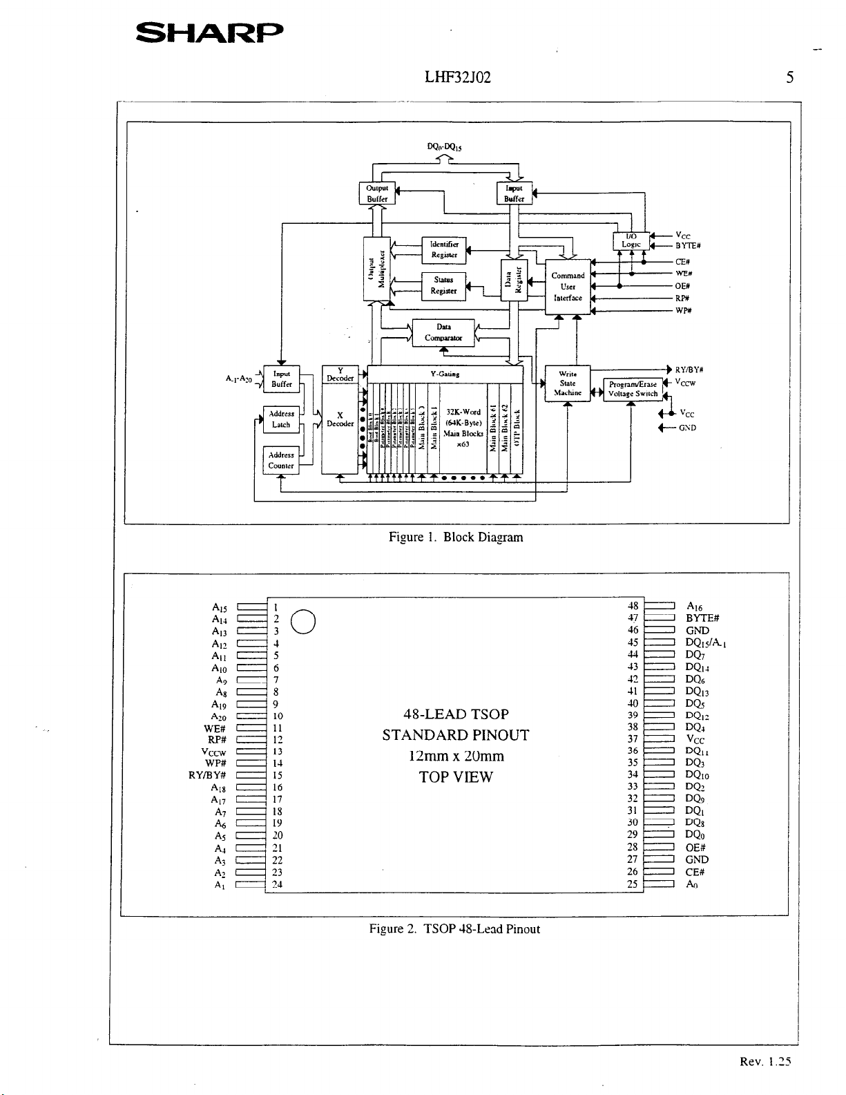
1.3 Product Description
1.3.1 Package Pinout
LH28F320BJE-PTTL90 Boot Block Flash memory is
available in 48-lead TSOP package (see Figure 2).
1.3.2 Block Organization
This product features an asymmetrically-blocked
architecture providing system memory integration. Each
erase block can be erased independently of the others up to
100,000 times. For the address locations of the blocks, see
the memory map in Figure 3.
Boot Blocks: The boot block is intended to replace a
dedicated boot PROM in a microprocessor or
microcontroller-based system. This boot block 4K words
(4,096words) features hardware controllable writeprotection to protect the crucial microprocessor boot code
from accidental modification. The protection of the boot
block is controlled using a combination of the V,,, RP#,
WP# pins and block lock-bit.
Parameter Blocks: The boot block architecture includes
parameter blocks to facilitate storage of frequently update
small parameters that would normally require an
EEPROM. By using software techniques, the word-rewrite
functionality of EEPROMs can be emulated. Each boot
block component contains six parameter blocks of JK
words (4.096 words) each. The protection of the parameter
block is controlled using a combination of the Vccw, RP#
and block lock-bit.
1
Main Blocks: The reminder is divided into main blocks for
data or code storage. Each 32M-bit device contains sixtythree 32K words (32.768 words) blocks. The protection of
the main block is controlled using a combination of the
Vccw. RP# and block lock-bit.
Rev. 1.X
r
--
LHF32JO2 5
Al5
Al4
43
Al?
All
40
A
‘48
A19
ho
WE#
RP#
vccw
WP#
RY/BY#
48
A17
2
AS
A4
A3
A?
Al
2
Ez 0
3
4
5
6
1
8
9
10
11
12
13
1-l
15
16
17
1s
19
20
21
22
23
24
Figure I. Block Diagram
48-LEAD TSOP
STANDARD PINOUT
12mm x 20mm
TOP VIEW
Figure 2. TSOP &Lead Pinout
48 I
47 I
45
44
43
42
41
40
39
38
37
36
35
34
33
32
31
Al6
BYTE#
GND
DQI~/AI
DQ7
DQIJ
DQs
DQu
W5
DQlz
DQI
vcc
DQII
DQ3
DQIO
DQz.
DQ9
DQI
DQs
DQo
OE#
GND
Cl3
‘%I
Rev. 1.2
SHARP
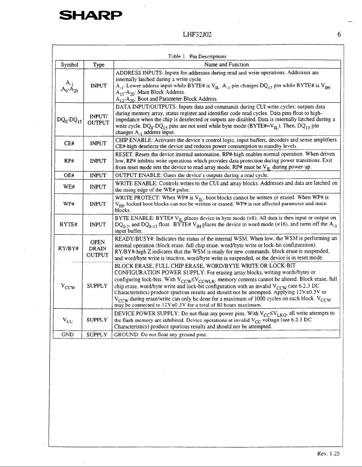
Symbol
A-1
A,-*20
1
DQ,-DQ,,
CE#
RP#
OE#
WE#
WI%
BYl-E#
RY/BY#
Vccw
vcc
GND
TYW
INPUT
INPUT/
OUTPUT
INPUT
INPUT
INPUT
INPUT
INPUT
INPUT
OPEN
DRAIN
OUTPUT
SUPPLY
SUPPLY
SUPPLY
LHF32JO2
Table 1. Pin Descriptions
Name and Function
ADDRESS INPUTS: Inputs for addresses during read and write operations. Addresses are
internally latched during a write cycle.
A-t: Lower address input while BYTE# is V,,. A-, pin changes DQ, j pin while BYTE# is V,,.
A, j-A20: Main Block Address.
A,1-A20: Boot and Parameter Block Address.
DATA INPUT/OUTPUTS: Inputs data and commands during CUI write cycles: outputs data
during memory array, status register and identifier code read cycles. Data pins float to highimpedance when the chip is deselected or outputs are disabled. Data is internally latched during a
write cycle. DQ*-DQtj pins are not used while byte mode (BYTE#=V,). Then. DQtj pin
changes A-, address input.
CHIP ENABLE: Activates the device’s control logic, input buffers, decoders and sense amplifiers.
CE#-high deselectsthe device and reduces power consumption to standby levels.
RESET: Resets the device internal automation. RP#-high enables normal operation. When driven
low, RP# inhibits write operations which provides data protection during power transitions. Exit
from reset mode sets the device to read array mode. RP# must be V, during power-up.
OUTPUT ENABLE: Gates the device’s outputs during a read cycle.
WRITE ENABLE: Controls writes to the CUI and array blocks. Addresses and data are latched on
the risine edge of the WE# uulse
WRITE PROTECT: When WP# is V,. boot blocks cannot be written or erased. When WP# is
V,, locked boot blocks can not be written or erased. WP# is not affected parameter and main
blocks.
BYTE ENABLE: BYTE# V, places device in byte mode (x8). All data is then input or output on
DQ,,. and DQs-, j float.
input buffer.
READY/BUSY#: Indicates the status of the internal WSM. When low, the WSM is performing an
internal operation (block erase, full chip erase, word/byte write or lock-bit configuration).
RY/BY#-high Z indicates that the WSM is ready for new commands. block erase is suspended.
and word/byte write is inactive, word/byte write is suspended, or the device is in reset mode.
BLOCK ERASE, FULL CHIP ERASE, WORD/BYTE WRITE OR LOCK-BIT
CONFIGURATION POWER SUPPLY: For erasing array blocks. writing words/bytes or
configuring lock-bits. With VCCWIVCCWLK. memory contents cannot be altered. Block erase, full
chip erase. word/byte write and lock-bit configuration with an invalid Vccw (see 6.2.3 DC
Characteristics) produce spurious results and should not be attempted. Applying 12V+O.3V to
Vccw during erase/write can only be done for a maximum of 1000 cycles on each block. Vccw
may be connected to 12V&.3V for a total of 80 hours maximum.
DEVICE POWER SUPPLY: Do not float any power pins. With V,,IV,,,, all write attempts to
the flash memory are inhibited. Device operations at invalid V,, voltage (see 6.2.3 DC
Characteristics) produce spurious results and should not be attempted.
GROUND: Do not float any ground pins.
BYTE# V,, places the device in word mode (x 16), and turns off the A-t
Rev. 1.25
SHARP
--
r
r
ho-A01 [AGO-A-II
32KW/64KB Mam Block
33KW/h-LKB Main Block
32KW/64KB Main Block
3?KW/h4KB Main Block
59 ‘I ::g
60 I ;;;z
61 1
62
LHF32J02
OEFWF
OEOQCO
ODFFFF
OCOCOO
OBFFFF
OBOIMO
OAFFFF
n . nnnn
OIFFFF
0 I two
CQmtT;
imoo
Top Boot
L%(rA(
EFlTF
iffooo
IFEFFF
II-E@Xl
IFDFFF
IFWOO
IFCFFF
IFCWO
IFBFFF
IFBCQO
IFAFFF
IFAOOO
ll?xFF
1F9m
IFSFFF
lF8lXKJ
lF7tFF
1’s
IEBMX)
lE7Ftl=
IEOWO
lDFFFl=
lD8KlC
lD7FFF
IWO00
ICFFFF
Ic8cixl
IUFFF
ICWOO
IBFFFF
IWOW
lB7FFF
IBoo
IAHFF
IA8000
lA7FFF
IALXXIO
19FFFF
l98cm
197FFF
190ooO
18FFFF
188cco
187FFF
18OooO
17FFFF
178000
177FFF
17ocQO
16tTFF
l68ONl
167lTF
16OGQO
15FFFF
lS8CCil
IVFFF
l5Oca
I.R=FF
I J8000
IUFFF
IUHXW)
IWFFF
138OW
137m
13OcQo
12FFFF
I28000
117FFF
IIOIXH
I I I-TFT
118000
117tTF
I IOocdI
I 0twF
108ooO
107tFF
ICWXX)
JKWIXKB Boot Block
_1. L”W
?FDFFF
‘FCOOO
3FBm
:r&E
3F8Mnl
3F7FFF
3F6000
3FSFFF
3MMX)
3F3FFF
3F1000
3FlFW
3FOiXMl
3EFFFF
3EOooO
3DFFFF
3wOQO
3cFFFF
3cmo
3BFFFF
3BCWO
3AFFFF
3AOCHl
39FFFF
390000
38FFFF
3scml
37FFFF
37oOm
36FFFF
36OMM
35FFFF
35OMx)
3aT-FF
?10000
33FFFF
330000
32tTF-F
310000
3lFFFF
31ooOQ
3oFFFF
3cQOm
?FFFFF
2FOOOO
EFFFF
lEOOO0
?DlTFF
JDCCCiI
2CFFFF
?CoooO
2BFtFF
?BooOO
MFFFF
2A0000
?9FFFF
19om
XWFFF
28OCUl
YFFFF
?7ccm
36FFFF
26OWX
25FFFF
250000
24=FFF
140000
I3FmF
230000
2ZFFFF
22oooo
1llTFF
210000
lOFFFF
30Ofl00
7
Figure 3. Memory Map
Rev. I.25
SHARI=
--
LHF32JO2
2 PRINCIPLES OF OPERATION
The LH28F320BIEPTTL90 Flash memory includes an
on-chip WSIM to manage block erase, full chip erase,
word/byte write and lock-bit configuration functions. It
allows for: fixed power supplies during block erase. full
chip erase, word/byte write and lock-bit configuration, and
minimal processor overhead with RAM-like interface
timings.
After initial device power-up or return from reset mode
(see section 3 Bus Operations). the device defaults to read
array mode. Manipulation of external memory control pins
allow array read, standby and output disable operations.
Status register and identifier codes can be accessed
through the CUI independent of the V,, voltage. High
voltage on V,, enables successful block erase, full chip
erase, word/byte write and lock-bit configurations. All
functions associated with altering memory contents-block
erase, full chip erase, word/byte write. lock-bit
zonfigurationt status and identifier codes-are accessed via
he CUI and verified through the status register.
Commands are written using standard microprocessor
write timings. The CUI contents serve as input to the
WSM, which controls the block erase, full chip erase,
word/byte write and lock-bit configuration. The internal
Algorithms are regulated by the WSM. including pulse
.epetition, internal verification and margining of data.
iddresses and data are internally latched during write
:ycles. Writing the appropriate command outputs array
lata, accesses the identifier codes or outputs status register
iata.
8
Interface software that initiates and polls progress of block
erase, full chip erase, word/byte write and lock-bit
configuration can be stored in any block. This code is
copied to and executed from system RAM during flash
memory updates. After successful completion, reads are
again possible via the Read Array command. Block erase
suspend allows system software to suspend a block erase
to read/write data from/to blocks other than that which is
suspend. Word/byte write suspend allows system software
to suspend a word/byte write to read data from any other
flash memory array location.
2.1 Data Protection
When V,&VccwLK.
altered. The CUI, with two-step block erase, full chip
erase, word/byte write or lock-bit configuration command
sequences, provides protection from unwanted operations
even when high voltage is applied to Vccw. All write
functions are disabled when V,, is below the write
lockout voltage V,,,
block locking capability provides additional protection
from inadvertent code or data alteration by gating block
erase. full chip erase and word/byte write operations.
Refer to Table 5 for write protection alternatives.
memory contents cannot be
or when RP# is at V,. The device’s
Rev. 1.25
SHARI=
--
LHF32JO2
3 BUS OPERATION
The local CPU reads and writes flash memory in-system.
All bus cycles to or from the flash memory conform to
standard microprocessor bus cycles.
3.; Read
Information can be read from any block, identifier codes
or status register independent of the Vccw voltage. RP#
can be at V,.
The first task is to write the appropriate read mode
command (Read Array. Read Identifier Codes or Read
Status Register) to the CUI. Upon initial device power-up
or after exit from reset mode. the device automatically
resets to read array mode. Six control pins dictate the data
flow in and out of the component: CE#, OE#, BYTE#,
WE#, RP# and WP#. CE# and OE# must be driven active
to obtain data at the outputs. CE# is the device selection
control. and when active enables the selected memory
device. OE# is the data output (DQo-DQ,,) control and
when active drives the selected memory data onto the I/O
bus. BYTE# is the device I/O interface mde control. WE#
must be at V,,, RP# must be at V,,. and BYTE# and WP#
must be at V, or V,,. Figure 16. 17 illustrates read cycle.
3.2 Output Disable
With OE# at a logic-high level (V,,). the device outputs
Ire disabled. Output pins (DQ,-DQ,j) are placed in a
ligh-impedance state.
3.3 Standby
9
3.4 Reset
RP# at V,, initiates the reset mode.
In read modes: RP#-low deselects the memory. places
output drivers in a high-impedance state and turns off all
internal circuits. RP# must be held low for a minimum of
1OOns. Time tpHQv
mode until initial memory access outputs are valid. After
this wake-up interval, normal operation is restored. The
CUI is reset to read array mode and status register is set to
80H.
During block erase. full chip erase. word/byte write or
lock-bit configuration modes. RP#-low will abort the
operation. RY/BY# remains low until the reset operation
is complete. Memory contents being altered are no longer
valid; the data may be partially erased or written. Time
tpBwL is required after RP# goes to logic-high (V,,)
before another command can be written.
As with any automated device. it is important to assert
RP# during system reset. When the system comes out of
reset, it expects to read from the flash memory. Automated
flash memories provide status information when accessed
during block erase. full chip erase, word/byte write or
lock-bit configuration modes. If a CPU reset occurs with
no flash memory reset. proper CPU initialization may not
occur because the flash memory may be providing status
information instead of
memories allow proper CPU initialization following a
system reset through the use of the RP# input. In this
application, RP# is controlled by the same RESET# signal
that resets the system CPU.
is required after return from reset
assay
data. SHARP’s flash
C1E# at a logic-high level (V,,) places the device in
standby mode which substantially reduces device power
:onsumption. DQ,-DQ,, outputs are placed in a high-
mpedance state independent of OE#. If deselected during
)lock erase. full chip erase. word/byte write or lock-bit
:onfiguration, the device continues functioning, and
:onsuming active power until the operation completes.
Rev. 1.15
SHARP
LHF32JO2 10
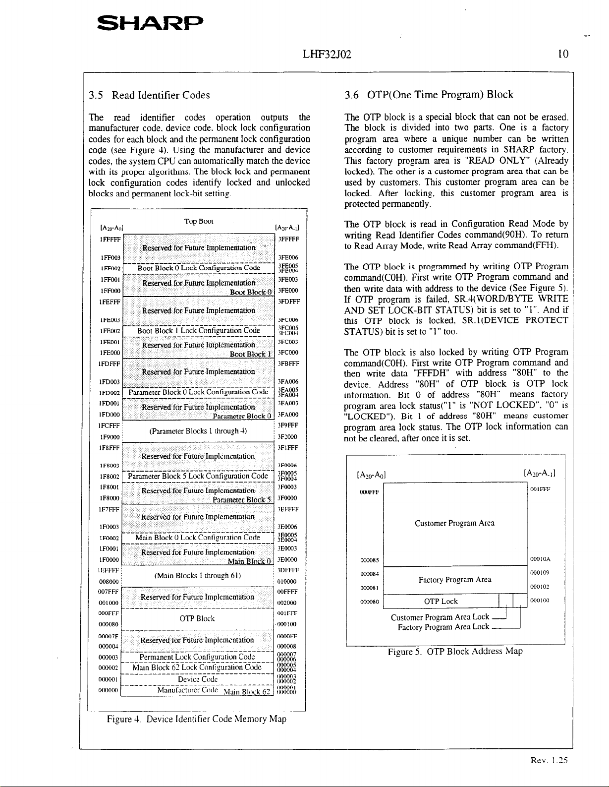
.5 Read Identifier Codes 3.6 OTP(One Time Program) Block
--
he read identifier codes operation outputs the
manufacturer code. device code.
block
lock configuration
Ides for each block and the permanent lock configuration
)de (see Figure 4). Using the manufacturer and device
Ides, the system CPU can automatically match the device
ith its proper algorithms. The block lock and permanent
mck configuration codes identify locked and unlocked
ocks and permanent lock-bit setting.
Top Boa
3FFFFF
3FEOO6
3FEOO5
3FEoo.t
3FEcm3
3FEOOO
3FDFFF
3FCCQ6
3FCOO5
3FCOO.t
3FCCO3
3FCMH)
3FBFFF
3FACC-5
3FAOO5
3FAOO.l
3FAOO3
3FACNM
IFCFFF;
IF9000 i
IFOWl
IFOiXQ
IEFFFF j i 3DFFFF
008000 i
(Parameter Blocks 1 through 4)
Reserved for Future Implementation
Parameter Block 5 Lock Confieumtion Code
~~__~_~^~~~~~-~l~----~---------~~-
Reserved for Future Implementr&ion
Main Block 0,
(Man Blocks 1 throyh 61)
Reserved forFuture Implementation
; 3F9FFF
; 3F1000
3FIFFF
3FMW6
3FooOS
3FOOOJ
3FOOO3
3FoooO
3EFFFF
3E0006
3EOOo5
3EOOOJ
3EOCO3
3EMXW)
The OTP block is a special block that can not be erased.
The block is divided into two parts. One is a factory
program area where a unique number can be written
according to customer requirements in SHARP factory.
This factory program area is “READ ONLY” (Already
locked). The other is a customer program area that can be
used by customers. This customer program area can be
locked. After locking, this customer program area is
protected permanently.
The OTP block is read in Configuration Read Mode by
writing Read Identifier Codes command(90H). To return
to Read Array Mode, write Read Array command(FFH).
The OTP block is programmed by writing OTP Program
command(COH). First write OTP Program command and
then write data with address to the device (See Figure 5).
If OTP program is failed, SR.J(WORD/BYTE WRITE
AND SET LOCK-BIT STATUS) bit is set to “1”. And if
this OTP block is locked, SR.I(DEVICE PROTECT
STATUS) bit is set to “1” too.
The OTP block is also locked by writing OTP Program
command(COH). First write OTP Program command and
then write data “FFFDH” with address “80H” to the
device. Address “80H” of OTP block is OTP lock
information. Bit 0 of address “80H” means factory
program area lock status(“1” is “NOT LOCKED”. “0” is
“LOCKED”). Bit 1 of address “SOH” means customer
program area lock status. The OTP lock information can
not be cleared, after once it is set.
ooom
Customer Program Area
1 oooO85 1
OOIFFF
1 OOOIOA j
000080 1
Figure 4. Device Identifier Code Memory Map
Customer Program Area Lock
Factory Program Area Lock
Figure 5. OTP Block Address Map
Rev. 1.35
SHARP
--
LHF32JO2 11
3.7 Write
Writing commands to the CUI enable reading of device
data and identifier codes. They also control inspection and
clearing of the status register. When V,,=2.7V-3.6V and
VCCW=VCCWH1/2~
erase, full chip erase, word/byte write and lock-bit
configuration.
The Block Erase command requires appropriate command
data and an address within the block to be erased. The Full
Chip Erase command requires appropriate command data
and an address within the device. The Word/Byte Write
command requires the command and address of the
location to be written. Set Permanent and Block Lock-Bit
commands require the command and address within the
device (Permanent Lock) or block within the device
(Block Lock) to be locked. The Clear Block Lock-Bits
command requires the command and address within the
device.
the CUI additionally controls block
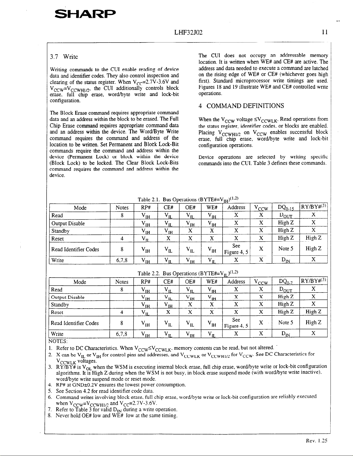
Table 2.1. Bus Operations (BYTEI
The CUI does not occupy an addressable memory
location. It is written when WE# and CE# are active. The
address and data needed to execute a command are latched
on the rising edge of WE# or CE# (whichever goes high
first). Standard microprocessor write timings are used.
Figures 18 and 19 illustrate WE# and CE# controlled write
operations.
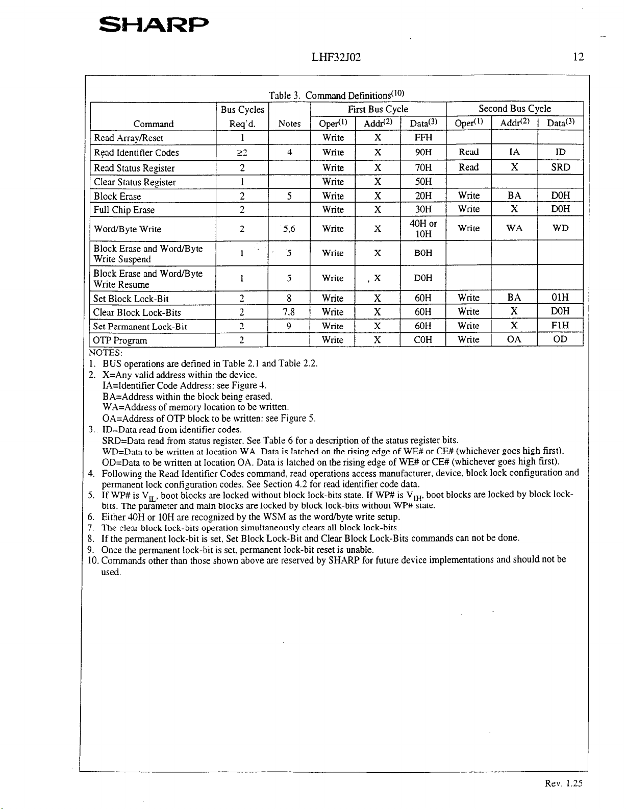
4 COMMAND DEFINITIONS
When the V,, voltage IVCCWLK. Read operations from
the status register, identifier codes. or blocks are enabled.
Placing VccWH1i2 on VCCW
erase. full chip erase. word/byte write and lock-bit
configuration operations.
Device operations are selected by writing specific
commands into the CUI. Table 3 defines these commands.
enables successful block
Read Identifier Codes
Write
673
VI, VI, VI, VIL
X X
DIN
X
NOTES:
1. Refer to DC Characteristics. When VccwlVccwLK.
memory contents can be read. but not altered. -
2. X can be V, or V,, for control pins and addresses, and VcCWLK or VCCWH,,2 for V,,,. See DC Characteristics for
VCCWLK voltages.
3. RY/BY# is V,, when the WSM is executing internal block erase, full chip erase, word/byte write or lock-bit configuration
algorithms. It is High Z during when the WSM is not busy, in block erase suspend mode (with word/byte write inactive).
word/byte write suspend mode or reset mode.
4. RP# at GND-cO.2V ensures the lowest power consumption.
5. See Section 4.2 for read identifier code data.
6. Command writes involving block erase, full chip erase, word/byte write or lock-bit configuration are reliably executed
when V
ccw=VccwHt/q and Vcc=2.7V-3.6V.
7. Refer to Table 3 for vahd D,, during a write operation,
8. Never hold OE# low and WE# low at the same timing.
Rev. 1.25
LHF32JO2 12
Table 3. Command Definition&lo)
--
Full Chip Erase
Word/Byte Write
II
Block Erase and Word/Byte
Write Suspend
Block Erase and Word/Byte
Write Resume
Set Block Lock-Bit
Clear Block Lock-Bits
Set Permanent Lock-Bit
OTP Program
1. BUS operations are defined in Table 2.1 and Table 2.2.
2. X=Any valid address within the device.
IA=Identifier Code Address: see Figure 4.
BA=Address within the block being erased.
WA=Address of memory location to be written.
OA=Address of OTP block to be written: see Figure 5.
3. ID=Data read from identifier codes.
SRD=Data read from status register. See Table 6 for a description of the status register bits.
WD=Data to be written at location WA. Data is latched on the rising edge of WE# or CE# (whichever goes high first).
OD=Data to be written at location OA. Data is latched on the rising edge of WE# or CE# (whichever goes high first).
4. Following the Read Identifier Codes command. read operations access manufacturer, device. block lock configuration and
permanent lock configuration codes. See Section 4.2 for read identifier code data.
5. If WP# is V,, boot blocks are locked without block lock-bits state. If WP# is Vt,,
bits. The parameter and main blocks are locked by block lock-bits without WP# state.
6. Either 4OH or 10H are recognized by the WSM as the word/byte write setup.
7. The clear block lock-bits operation simultaneously clears all block lock-bits.
8. If the permanent lock-bit is set, Set Block Lock-Bit and Clear Block Lock-Bits commands can not be done.
9. Once the permanent lock-bit is set. permanent lock-bit reset is unable.
10. Commands other than those shown above are reserved by SHARP for future device implementations and should not be
used.
2
2 1 5.6
I
1 > .j
1
2
2
2 9 Write X 60H Write X FIH
2 Write X COH Write OA OD
1 Write 1 X 1 30H 1 Write 1 X ) DOH
1 Write I x ) 4yy~ I Write I WA / WD I /
Write X BOH
5 Write , X
8
7.8
Write X 60H
Write X 60H Write X DOH
I
DOH
Write
boot blocks are locked by block lock-
BA
OlH
I
Rev. 1.25
SHARP
LHF32JO2
4.1 Read Array Command
Upon initial device power-up and after exit from reset
mode. the device defaults to read array mode. This
operation is also initiated by writing the Read Array
command. The device remains enabled for reads until
another command is written. Once the internal WSM has
started a block erase, full chip erase. word/byte write or
lock-bit configuration the device will not recognize the
Read Array command until the WSM completes its
operation unless the WSM is suspended via an Erase
Suspend or Word/Byte Write Suspend command. The
Read Array command functions independently of the
Vccw voltage and RP# can be V,,.
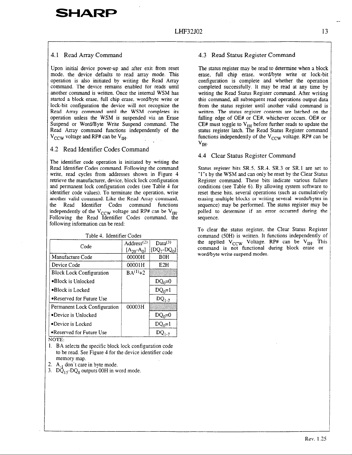
4.2 Read Identifier Codes Command
The identifier code operation is initiated by writing the
Read Identifier Codes command. Following the command
write, read cycles from addresses shown in Figure 4
retrieve the manufacturer, device. block lock configuration
and permanent lock configuration codes (see Table 4 for
Identifier code values). To terminate the operation. write
another valid command. Like the Read Array command,
he Read Identifier Codes command functions
ndependently of the V,-w voltage and RP# can be V,,.
‘allowing the Read Identifier Codes command, the
‘allowing information can be read:
Table 4. Identifier Codes
Code
Manufacture Code
Device Code
Block Lock Configuration
*Block is Unlocked
*Block is Locked
*Reserved for Future Use
Permanent Lock Configuration
Address(‘)
[A,,-A,1 PQ,-DQ,l
OOOOOH BOH
OOOOlH E2H
B A( I,+2 ‘~~~~~~~
Data(3)
.,...
DQ,=O
DQ,= 1
., ,.
4.3 Read Status Register Command
The status register may be read to determine when a block
erase, full chip erase, word/byte write or lock-bit
configuration is complete and whether the operation
completed successfully. It may be read at any time by
writing the Read Status Register command. After writing
this command, all subsequent read operations output data
from the status register until another valid command is
written. The status register contents are latched on the
falling edge of OE# or CE#, whichever occurs. OE# or
CE# must toggle to VIH before further reads to update the
status register latch. The Read Status Register command
functions independently of the Vccw voltage. RP# can be
VII-t.
4.4 Clear Status Register Command
Status register bits SR.5. SR.4. SR.3 or SR.l are set to
“1”s by the WSM and can only be reset by the Clear Status
Register command. These bits indicate various failure
conditions (see Table 6). By allowing system software to
reset these bits. several operations (such as cumulatively
erasing multiple blocks or writing several words/bytes in
sequence) may be performed. The status register may be
polled to determine if an error occurred during the
sequence.
To clear the status register. the Clear Status Register
command (50H) is written. It functions independently of
the applied Vccw
command is not functional during block erase or
word/byte write suspend modes.
Voltage. RP# can be V,,. This
BA selects the specific block lock configuration code
to be read. See Figure 4 for the device identifier code
memory map.
!. A-, don’t care in byte mode.
1. DQtj-DQ9 outputs OOH in word mode.
Rev.
_I
1.25

SHARP
LHF32JO2
4.5 Block Erase Command
Erase is executed one block at a time and initiated by a
two-cycle command. A block erase setup is first written,
followed by an block erase confirm. This command
sequence requires appropriate sequencing and an address
within the block to be erased (erase changes all block data
to FFFFH/FFH). Block preconditioning. erase. and verify
are handled internally by the WSM (invisible to the
system). After the two-cycle block erase sequence is
written, the device automatically outputs status register
data when read (see Figure 6). The CPU can detect block
erase completion by analyzin_g the output data of the
RY/BY# pin or status register bit SR.7.
When the block erase is complete, status register bit SR.5
should be checked. If a block erase error is detected, the
status register should be cleared before system software
attempts corrective actions. The CUI remains in read
status register mode until a new command is issued.
This two-step command sequence of set-up followed by
execution ensures that block contents are not accidentally
erased. An invalid Block Erase command sequence will
result in both status register bits SR.4 and SR.5 being set
to “1”. Also. reliable block erasure can only occur when
Vcc=2.7V-3.6V and VCCW=VCCwH1,?. In the absence of
this high voltage, block contents are protected against
erasure. If block erase is attempted while VCCWIVCCWLK.
SR.3 and SR.5 will be set to “1”. Successful block erase
requires for boot blocks that WP# is V,, and the
corresponding block lock-bit be cleared. In parameter and
main blocks case, it must be cleard the corresponding
block lock-bit. If block erase is attempted when the
excepting above conditions. SR.1 and SR.5 will be set to
“1”.
4.6 Full Chip Erase Command
I’his command followed by a confirm command erases all
af the unlocked blocks. A full chip erase setup (30H) is
!irst written. followed by a full chip erase confirm (DOH).
4fter a confirm command is written. device erases the all
mlocked blocks block by block. This command sequence
.equires appropriate sequencing. Block preconditioning.
:rase and verify are handled internally by the WSIM
invisible to the system). After the two-cycle full chip
:rase sequence is written. the device automatically outputs
status register data when read (see Figure 7). The CPU can
ietect full chip erase completion by analyzing the output
lata of the RY/BY# pin or status register bit SR.7.
Nhen the full chip erase is complete. status register bit
lR.5 should be checked. If erase error is detected. the
tatus register should be cleared before system software
ittempts corrective actions. The CUI remains in read
status register mode until a new command is issued. I
error is detected on a block during full chip erase
operation. WSIM stops erasing. Full chip erase operatior
start from lower address block. finish the higher addres!
block. Full chip erase can not be suspended.
This two-step command sequence of set-up followed b)
execution ensures that block contents are not accidentall)
erased. An invalid Full Chip Erase command sequence
will result in both status register bits SR.4 and SR.5 being
set to “1”. Also, reliable full chip erasure can only
when V,,absence of this high voltage. block contents are protectec
against erasure. If full chip erase is attempted while
V CCWIVCCwrK. SR.3 and SR.5 will be set to “1”
Successful full chip erase requires for boot blocks thal
WP# is V,, and the corresponding block lock-bit be
cleared. In parameter and main blocks case, it must be
cleard the corresponding block lock-bit. If all blocks are
locked. SR.1 and SR.5 will be set to “1”.
-2 7V-3.6V and VCCw=VCCWHln. In the
OCCUI
4.7 Word/Byte Write Command
Word/Byte write is executed by a two-cycle command
sequence. Word/Byte write setup (standard 40H 01
alternate 10H) is written. followed by a second write that
specifies the address and data (latched on the rising edge
of WE#). The WSM then takes over, controlling the
word/byte write and write verify algorithms internally.
After the word/byte write sequence is written, the device
automatically outputs status resister data when read (see
Figure 8). The CPU can detect the completion of the
word/byte write event by analyzing the RY/BY# pin OI
status register bit SR.7.
When word/byte write is complete, status register bit SR.J
should be checked. If word/byte write error is detected. the
status register should be cleared. The internal WSM verify
only detects errors for “1”s that do not successfully write
to “0”s. The CUI remains in read status register mode until
it receives another command.
Reliable word/byte writes can only occur when
V,,=2.7V-3.6V and VCCw=VCCWHIR. In the absence of
this high voltage. memory contents are protected against
word/byte writes. If word/byte write is attempted while
VCCW<VCCwtK. status register bits SR.3 and SR.4 will be
set to “I”. Successful word/byte write requires for boot
blocks that WP# is V,, and the corresponding block lockbit be cleared. In parameter and main blocks case, it must
be cleard the corresponding block lock-bit. If word/byte
write is attempted when the excepting above conditions.
SR. 1 and SR.-l will be set to “I”.
Rev. 1.25
 Loading...