

Sharp LH28F160SGED-L10 Datasheet
16 M-bit (512 kB x 16 x 2-Bank)
LH28F160SGED-L10
DESCRIPTION
The LH28F160SGED-L10 Dual Work flash memory
with SmartVoltage technology is a high-density,
low-cost, nonvolatile, read/write storage solution for
a wide range of applications. The LH28F160SGEDL10 is the highest density, highest performance
non-volatile read/write solution for solid-state
storage applications. LH28F160SGED-L10 can
read/write/erase at V
Its low voltage operation capability realizes longer
battery life and suits for cellular phone application.
Its symmetrically-blocked architecture, flexible
voltage and enhanced cycling capability provide for
highly flexible component suitable for resident flash
arrays, SIMMs and memory cards. Its enhanced
suspend capabilities provide for an ideal solution for
code + data storage applications. For secure code
storage applications, such as networking, where
code is either directly executed out of flash or
downloaded to DRAM, the LH28F160SGED-L10
offers three levels of protection : absolute protection
PP at GND, selective hardware block locking,
with V
or flexible software block locking. These alternatives
give designers ultimate control of their code security
needs.
FEATURES
• SmartVoltage Dual Work technology
– 2.7 V, 3.3 V or 5 V V
– 2.7 V, 3.3 V, 5 V or 12 V VPP
– Capable of performing erase, write and read
for each bank independently (Impossible to
perform read from both banks at a time).
• High performance read access time
– 100 ns (5.0±0.5 V)/100 ns (3.3±0.3 V)/
120 ns (2.7 to 3.6 V)
CC = 2.7 V and VPP = 2.7 V.
CC
SmartVoltage Dual Work Flash Memory
• Enhanced automated suspend options
– Word write suspend to read
– Block erase suspend to word write
– Block erase suspend to read
• Enhanced data protection features
– Absolute protection with V
– Flexible block locking
– Block erase/word write lockout during power
transitions
• SRAM-compatible write interface
• High-density symmetrically-blocked architecture
– Thirty-two 32 k-word erasable blocks
• Enhanced cycling capability
– 100 000 block erase cycles
– 1.6 million block erase cycles/bank
• Low power management
– Deep power-down mode
– Automatic power saving mode decreases Icc
in static mode
• Automated word write and block erase
– Command user interface
– Status register
TM
∗
• ETOX
• Package
– 48-pin TSOP Type I (TSOP048-P-1220)
∗ ETOX is a trademark of Intel Corporation.
V nonvolatile flash technology
LH28F160SGED-L10
PP = GND
Normal bend
In the absence of confirmation by device specification sheets, SHARP takes no responsibility for any defects that may occur in equipment using any SHARP devices shown in catalogs, data books,
etc. Contact SHARP in order to obtain the latest device specification sheets before using any SHARP device.
- 1 -
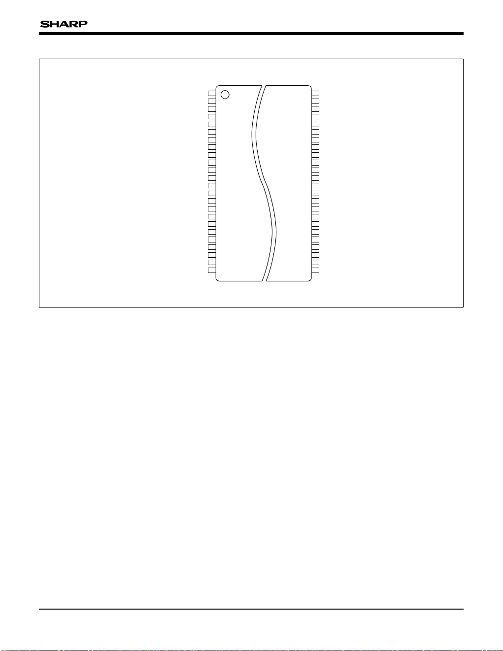
PIN CONNECTIONS
48-PIN TSOP (Type I)
(TSOP048-P-1220)
A15
A14
A13
A12
A11
A10
A9
A8
NC
NC
WE#
RP#
V
PP
WP#
NC
A
18
A17
A7
A6
A5
A4
A3
A2
A1
1
2
3
4
5
6
7
8
9
10
11
12
13
14
15
16
17
18
19
20
21
22
23
24
48
47
46
45
44
43
42
41
40
39
38
37
36
35
34
33
32
31
30
29
28
27
26
25
A16
GND
DQ
15
DQ7
DQ14
DQ6
DQ13
DQ5
DQ12
DQ4
VCC
DQ11
DQ3
DQ10
DQ2
DQ9
DQ1
DQ8
DQ0
OE#
GND
BE
1#
BE
0#
A
0
LH28F160SGED-L10
TOP VIEW
- 2 -
BLOCK DIAGRAM
Bank0
Bank1
DQ0-DQ
15
VCC
WE#
OE#
WP#
RP#
A0-A
18
VCC
GND
V
PP
BE1#
BE
0#
I/O
LOGIC
COMMAND
USER
INTERFACE
INPUT
BUFFER
DATA
REGISTER
WRITE
STATE
MACHINE
PROGRAM/ERASE
VOLTAGE SWITCH
IDENTIFIER
REGISTER
OUTPUT
BUFFER
Y GATING
DATA
COMPARATOR
STATUS
REGISTER
OUTPUT
MULTIPLEXER
16
32 k-WORD
BLOCKS
Y DECODER
INPUT
BUFFER
ADDRESS
LATCH
ADDRESS
COUNTER
X DECODER
LH28F160SGED-L10
- 3 -
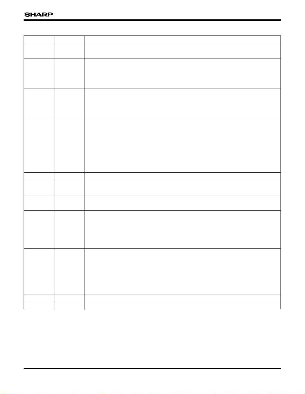
PIN DESCRIPTION
SYMBOL TYPE NAME AND FUNCTION
A
0-A18 INPUT
DQ0-DQ15
0#,
BE
BE1#
RP#
INPUT/
OUTPUT
INPUT
INPUT
OE# INPUT OUTPUT ENABLE : Controls the device's outputs during a read cycle.
WE# INPUT
WP# INPUT
V
PP
SUPPLY
VCC SUPPLY
GND SUPPLY GROUND : Do not float any ground pins.
NC NO CONNECT : Lead is not internal connected; recommend to be floated.
ADDRESS INPUTS : Inputs for addresses during read and write operations. Addresses
are internally latched during a write cycle.
DATA INPUT/OUTPUTS : Inputs data and commands during CUI write cycles; outputs
data during memory array, status register, and identifier code read cycles. Data pins
float to high-impedance when the chip is deselected or outputs are disabled. Data is
internally latched during a write cycle.
BANK ENABLE : Activates the device’s control logic, input buffers, decoders, and
sense amplifiers. When BE
0# are "low", bank0 is in active. When BE1# are "low", bank1
is in active. Both BE0# and BE1# must not be low at the same time. BE0#, BE1#-high
deselects the device and reduces power consumption to standby levels.
RESET/DEEP POWER-DOWN : Puts the device in deep power-down mode and resets
internal automation. RP#-high enables normal operation. When driven low, RP# inhibits
write operations which provide data protection during power transitions. Exit from deep
power-down sets the device to read array mode.
RP# at V
configuration with V
HH allows to set permanent lock-bit. Block erase, word write, or lock-bit
IH ≤ RP# ≤ VHH produce spurious results and should not be
attempted.
WRITE ENABLE : Controls writes to the CUI and array blocks. Addresses and data are
latched on the rising edge of the WE# pulse.
When V
WRITE PROTECT : Master control for block locking.
IL, locked blocks cannot be
erased and programmed, and block lock-bits cannot be set and reset.
BLOCK ERASE, WORD WRITE, LOCK-BIT CONFIGURATION POWER SUPPLY :
For erasing array blocks, writing words, or configuring lock-bits. With V
memory contents cannot be altered. Block erase, word write, and lock-bit configuration
with an invalid V
PP (see Section 6.2.3 "DC CHARACTERISTICS") produce spurious
results and should not be attempted.
DEVICE POWER SUPPLY : Internal detection configured the device for 2.7 V, 3.3 V or
5 V operation. To switch from one voltage to another, ramp V
CC to the new voltage. Do not float any power pins. With VCC ≤ VLKO, all write
ramp V
CC down to GND and then
attempts to the flash memory are inhibited. Device operations at invalid VCC voltage
(see Section 6.2.3 "DC CHARACTERISTICS") produce spurious results and should
not be attempted.
LH28F160SGED-L10
PP ≤ VPPLK,
- 4 -

1 INTRODUCTION
This datasheet contains LH28F160SGED-L10
specifications. Section 1 provides a flash memory
overview. Sections 2, 3, 4, and 5 describe the
memory organization and functionality. Section 6
covers electrical specifications. LH28F160SGEDL10 flash memory documentation also includes
ordering information which is referenced in
Section 7.
1.1 New Features
Key enhancements of LH28F160SGED-L10
SmartVoltage Dual Work flash memory are :
• SmartVoltage Dual Work Technology
• Enhanced Suspend Capabilities
• In-System Block Locking
• Permanent Lock Capability
Note following important differences :
PPLK has been lowered to 1.5 V to support
•V
3.3 V and 5 V block erase, word write, and lockbit configuration operations. Designs that switch
PP off during read operations should make sure
V
that the V
PP voltage transitions to GND.
• To take advantage of SmartVoltage technology,
allow V
CC connection to 2.7 V, 3.3 V or 5 V.
• Once set the permanent lock bit, the blocks
which have been set block lock-bit can not be
erased, written forever.
1.2 Product Overview
The LH28F160SGED-L10 is a high-performance
16 M-bit SmartVoltage Dual Work flash memory
organized as 1 024 k-word of 16 bits. The 1 024 kword of data is arranged in thirty-two 32 k-word
blocks which are individually erasable, lockable,
and unlockable in-system. The memory map is
shown in Fig. 1.
LH28F160SGED-L10
select one of banks. BE
pin which is CE# in LH28F800SGE-L10, BE
is assigned to No. 27 pin which is GND in
LH28F800SGE-L10. To select either bank (bank0)
0# must be "L", and to select another bank
BE
(bank1) BE
1# must be "L". Selecting both banks
(bank0 and bank1) at a time, except of read
operation (array read, status register read), turns
both BE
0# and BE1# to "L".
Operation mode of bank0 and bank1 as follows :
1) Both bank0 and bank1 are in deep power-down
(RP# = "L").
2) Both bank0 and bank1 are in standby
0# = BE1# = "H").
(BE
3) Bank0 is in standby and bank1 is in active state
of programming or erase, or bank0 is in active
state of programming or erase and bank1 is in
standby.
4) Both bank0 and bank1 are in active state
(impossible to perform simultaneous read from
both banks). In this case bank0 and bank1
perform independent operation, for example,
after input Erase command to bank0 erase or
program command to bank1 is succeeded,
bank0 and bank1 perform each operation
concurrently.
SmartVoltage technology provides a choice of V
and VPP combinations, as shown in Table 1, to
meet system performance and power expectations.
2.7 to 3.6 V V
CC consumes approximately one-fifth
the power of 5 V V
highest read performance. V
eliminates the need for a separate 12 V converter,
PP = 12 V maximizes block erase and word
while V
write performance. In addition to flexible erase and
program voltages, the dedicated V
complete data protection when V
0# is assigned to No. 26
1#
CC
CC. But, 5 V VCC provides the
PP at 3.3 V and 5 V
PP pin gives
PP ≤ VPPLK.
All pins except of BE# are shared by both banks,
and BE# is divided to BE
0# and BE1# in order to
- 5 -
LH28F160SGED-L10
Table 1 VCC and VPP Voltage Combinations
Offered by SmartVoltage Technology
VCC VOLTAGE VPP VOLTAGE
2.7 V 2.7 V, 3.3 V, 5 V, 12 V
3.3 V 3.3 V, 5 V, 12 V
5 V 5 V, 12 V
Internal VCC and VPP detection circuitry automatically configures the device for optimized read
and write operations.
A command User Interface (CUI) serves as the
interface between the system processor and
internal operation of the device. A valid command
sequence written to the CUI initiates device
automation. An internal Write State Machine (WSM)
automatically executes the algorithms and timing
necessary for block erase, word write, and lock-bit
configuration operations.
A block erase operation erases one of the device’s
32 k-word blocks typically within 1.2 second (5 V
CC, 12 V VPP) independent of other blocks. Each
V
block can be independently erased 100 000 times
(1.6 million block erases per device). Block erase
suspend mode allows system software to suspend
block erase to read data from, or write data to any
other block.
Writing memory data is performed in word
increments typically within 7.5 µs (5 V V
V
PP). Word write suspend mode enables the
CC, 12 V
system to read data from, or write data to any other
flash memory array location.
The selected block can be locked or unlocked
individually by the combination of thirty-two block
lock bits and the RP# or WP#. Block erase or word
write must not be carried out by setting block lock
bits and setting WP# to low and RP# to V
if WP# is high state or RP# is set to V
IH. Even
HH, block
erase and word write to locked blocks is prohibited
by setting permanent lock bit.
In each bank0, 1 contains of Status Registers. The
status register indicates when the WSM’s block
erase, word write, or lock-bit configuration operation
is finished.
The LH28F160SGED-L10 also incorporates a dual
bank-enable function with two input pins, BE
1#. For minimum chip designs, BE0# may be
BE
tied to ground and use BE
1# as the bank enable
0# and
input. The LH28F160SGED-L10 uses the logical
combination of these two signals to enable or
disable the entire chip. Both BE
0# and BE1# must
be active low to enable the device and if either one
becomes inactive, the bank will be disabled. This
feature allows the system designer to reduce the
number of control pins used in a large array of
16 M-bit devices.
The access time is 100 ns (t
AVQV) at the VCC
supply voltage range of 4.5 to 5.5 V over the
temperature range, –10 to +70˚C. At lower V
CC
voltage, the access time is 100 ns (3.0 to 3.6 V)
and 120 ns (2.7 to 3.6 V).
The Automatic Power Saving (APS) feature
substantially reduces active current when the
device is in static mode (addresses not switching).
In APS mode, the typical I
CC and 3 mA at 2.7 to 3.6 V VCC, both
5 V V
CCR current is 1 mA at
bank0, 1 are in active state.
When BE# and RP# pins are at V
CC, the ICC
CMOS standby mode is enabled. When the RP#
pin is at GND, deep power-down mode is enabled
which minimizes power consumption and provides
write protection during reset. A reset time (t
PHQV) is
required from RP# switching high until outputs are
valid. Likewise, the device has a wake time (t
PHEL)
from RP#-high until writes to the CUI are
recognized. With RP# at GND, the WSM is reset
and the status register is cleared.
- 6 -
LH28F160SGED-L10
32 k-Word Block
32 k-Word Block
32 k-Word Block
32 k-Word Block
32 k-Word Block
32 k-Word Block
32 k-Word Block
32 k-Word Block
32 k-Word Block
32 k-Word Block
32 k-Word Block
32 k-Word Block
32 k-Word Block
32 k-Word Block
32 k-Word Block
32 k-Word Block
15
14
13
12
11
10
9
8
7
6
5
4
3
2
1
0
7FFFF
78000
77FFF
70000
6FFFF
67FFF
68000
60000
5FFFF
58000
57FFF
50000
4FFFF
48000
47FFF
40000
3FFFF
38000
37FFF
30000
2FFFF
28000
27FFF
20000
1FFFF
18000
17FFF
10000
0FFFF
08000
07FFF
00000
32 k-Word Block
32 k-Word Block
32 k-Word Block
32 k-Word Block
32 k-Word Block
32 k-Word Block
32 k-Word Block
32 k-Word Block
32 k-Word Block
32 k-Word Block
32 k-Word Block
32 k-Word Block
32 k-Word Block
32 k-Word Block
32 k-Word Block
32 k-Word Block
15
14
13
12
11
10
9
8
7
6
5
4
3
2
1
0
7FFFF
78000
77FFF
70000
6FFFF
67FFF
68000
60000
5FFFF
58000
57FFF
50000
4FFFF
48000
47FFF
40000
3FFFF
38000
37FFF
30000
2FFFF
28000
27FFF
20000
1FFFF
18000
17FFF
10000
0FFFF
08000
07FFF
00000
Bank0
(BE
0# = "L")
Bank1
(BE1# = "L")
Fig.1 Memory Map
2 PRINCIPLES OF OPERATION
The LH28F800SGE-L10 SmartVoltage Dual Work
flash memory includes an on-chip WSM to manage
block erase, word write, and lock-bit configuration
functions. It allows for 100% TTL-level : control
inputs, fixed power supplies during block erasure,
word write, and lock-bit configuration, and minimal
processor overhead with RAM-like interface timings.
After initial device power-up or return from deep
power-down mode (see Table 2 "Bus Operations"),
the device defaults to read array mode.
Manipulation of external memory control pins allow
array read, standby, and output disable operations.
Status register and identifier codes can be
accessed through the CUI independent of the V
voltage. High voltage on VPP enables successful
PP
block erasure, word writing, and lock-bit
configuration. All functions associated with altering
memory contents—block erase, word write, lock-bit
configuration, status, and identifier codes—are
accessed via the CUI and verified through the
status register.
Commands are written using standard microprocessor write timings. The CUI contents serve as
input to the WSM, which controls the block erase,
word write, and lock-bit configuration. The internal
algorithms are regulated by the WSM, including
pulse repetition, internal verification, and margining
of data. Addresses and data are internally latched
during write cycles. Writing the appropriate
command outputs array data, accesses the
identifier codes, or outputs status register data.
- 7 -

LH28F160SGED-L10
Interface software that initiates and polls progress
of block erase, word write, and lock-bit configuration
can be stored in any block. This code is copied to
and executed from system RAM during flash
memory updates. After successful completion,
reads are again possible via the Read Array
command. Block erase suspend allows system
software to suspend a block erase to read/write
data from/to blocks other than that which is
suspended. Word write suspend allows system
software to suspend a word write to read data from
any other flash memory array location.
2.1 Data Protection
Depending on the application, the system designer
may choose to make the V
switchable (available only when memory block
erases, word writes, or lock-bit configurations are
required) or hardwired to V
accommodates either design practice and
encourages optimization of the processor-memory
interface.
When V
PP ≤ VPPLK, memory contents cannot be
altered. The CUI, with two-step block erase, word
write, or lock-bit configuration command sequences,
provides protection from unwanted operations even
when high voltage is applied to V
functions are disabled when V
lockout voltage V
LKO or when RP# is at VIL. The
device’s block locking capability provides additional
protection from inadvertent code or data alteration
by gating erase and word write operations.
PP power supply
PPH1/2/3. The device
PP. All write
CC is below the write
The first task is to write the appropriate read mode
command (Read Array, Read Identifier Codes, or
Read Status Register) to the CUI. Upon initial
device power-up or after exit from deep powerdown mode, the device automatically resets to read
array mode. Five control pins dictate the data flow
in and out of the component : BE#, OE#, WE#,
RP# and WP#. BE# and OE# must be driven
active to obtain data at the outputs. BE# is the
device selection control, and when active enables
the selected memory device. OE# is the data
output (DQ
0-DQ15) control and when active drives
the selected memory data onto the I/O bus. WE#
must be at V
IH and RP# must be at VIH or VHH.
Fig. 13 illustrates read cycle.
3.2 Output Disable
With OE# at a logic-high level (VIH), the device
outputs are disabled. Output pins DQ
0-DQ15 are
placed in a high-impedance state.
3.3 Standby
BE# at a logic-high level (VIH) places the device in
standby mode which substantially reduces device
power consumption. DQ
0-DQ15 outputs are placed
in a high-impedance state independent of BE#. If
deselected during block erase, word write, or lockbit configuration, the device continues functioning,
and consuming active power until the operation
completes.
3.4 Deep Power-Down
RP# at VIL initiates the deep power-down mode.
3 BUS OPERATION
The local CPU reads and writes flash memory insystem. All bus cycles to or from the flash memory
conform to standard microprocessor bus cycles.
3.1 Read
Information can be read from any block, identifier
codes, or status register independent of the V
voltage. RP# can be at either VIH or VHH.
PP
In read modes, RP#-low deselects the memory,
places output drivers in a high-impedance state and
turns off all internal circuits. RP# must be held low
for a minimum of 100 ns. Time t
PHQV is required
after return from power-down until initial memory
access outputs are valid. After this wake-up interval,
normal operation is restored. The CUI is reset to
read array mode and status register is set to 80H.
- 8 -
LH28F160SGED-L10
7FFFF
78004
78003
78002
78001
78000
0FFFF
08004
08003
08002
08001
08000
07FFF
00004
00003
00002
00001
00000
Reserved for
Future Implementation
Reserved for
Future Implementation
Reserved for
Future Implementation
Reserved for
Future Implementation
Reserved for
Future Implementation
Block 15 Lock Configuration Code
Block 15
Block 1
Block 0
(Blocks 2 through 14)
Block 1 Lock Configuration Code
Permanent Lock Configuration Code
Block 0 Lock Configuration Code
Device Code
Manufacture Code
Bank0
(BE
0# = "L")
7FFFF
78004
78003
78002
78001
78000
0FFFF
08004
08003
08002
08001
08000
07FFF
00004
00003
00002
00001
00000
Block 15 Lock Configuration Code
Block 15
Block 1
Block 0
(Blocks 2 through 14)
Block 1 Lock Configuration Code
Permanent Lock Configuration Code
Block 0 Lock Configuration Code
Device Code
Manufacture Code
Bank1
(BE
1# = "L")
Reserved for
Future Implementation
Reserved for
Future Implementation
Reserved for
Future Implementation
Reserved for
Future Implementation
Reserved for
Future Implementation
During block erase, word write, or lock-bit
configuration modes, RP#-low will abort the operation.
Memory contents being altered are no longer valid;
the data may be partially erased or written. Time
t
PHWL is required after RP# goes to logic-high (VIH)
before another command can be written.
As with any automated device, it is important to
assert RP# during system reset. When the system
comes out of reset, it expects to read from the flash
memory. Automated flash memories provide status
information when accessed during block erase,
word write, or lock-bit configuration modes. If a
CPU reset occurs with no flash memory reset,
proper CPU initialization may not occur because
the flash memory may be providing status
information instead of array data. SHARP’s flash
memories allow proper CPU initialization following a
system reset through the use of the RP# input. In
this application, RP# is controlled by the same
RESET# signal that resets the system CPU.
3.5 Read Identifier Codes
The read identifier codes operation outputs the
manufacture code, device code, block lock
configuration codes for each block, and the
permanent lock configuration code (see Fig. 2).
Using the manufacture and device codes, the
system CPU can automatically match the device
with its proper algorithms. The block lock and
permanent lock configuration codes identify locked
and unlocked blocks and permanent bank lock-bit
setting.
Fig. 2 Device Identifier Code Memory Map
- 9 -
LH28F160SGED-L10
3.6 Write
Writing commands to the CUI enable reading of
device data and identifier codes. They also control
inspection and clearing of the status register.
The Block Erase command requires appropriate
command data and an address within the block to
be erased. The Word Write command requires the
command and address of the location to be written.
Set Permanent Bank and Block Lock-Bit
commands require the command and address
within the device (Permanent Bank Lock) or block
within the device (Block Lock) to be locked. The
Clear Block Lock-Bits command requires the
command and address within the device.
The CUI does not occupy an addressable memory
location. It is written when WE# and BE# are
Table 2 Bus Operations
MODE NOTE RP# BE0#BE1# OE# WE#
Bank0
Read Bank1
Disable VIL VIL
Output Disable
Bank0
Standby Bank1
Bank0, 1 VIH VIH
1, 2, V
7, 8 V
V
IH
V
IH or
HH
or VHHXXVIH VIH X X High Z
IH or
V
HH
Deep Power-Down 3 VIL X X X X X X High Z
Bank0
Read Identifier Codes Bank1 7, 8
Disable VIL VIL
Bank0
Write Bank1 5, 6, 7
Bank0, 1 VIL VIL
V
V
IH or
HH
V
IH or
V
HH
NOTES :
1. Refer to Section 6.2.3 "DC CHARACTERISTICS".
When V
PP ≤ VPPLK, memory contents can be read, but
not altered.
2. X can be V
V
PPLK or VPPH1/2/3 for VPP. See Section 6.2.3 "DC
CHARACTERISTICS" for V
3. RP# at GND±0.2 V ensures the lowest deep powerdown current.
IL or VIH for control pins and addresses, and
PPLK and VPPH1/2/3 voltages.
active. The address and data needed to execute a
command are latched on the rising edge of WE# or
BE# (whichever goes high first). Standard
microprocessor write timings are used. Fig. 14 and
Fig. 15 illustrate WE# and BE# controlled write
operations.
4 COMMAND DEFINITIONS
When the VPP ≤ VPPLK, read operations from the
status register, identifier codes, or blocks are
enabled. Placing V
successful block erase, word write and lock-bit
configuration operations.
Device operations are selected by writing specific
commands into the CUI. Table 3 defines these
commands.
IL VIH
V
VIH VIL VIL VIH XXDOUT
IH VIL
V
VIL VIH X X X X High Z
IL VIH
V
VIH VIL VIL VIH
IL VIH
V
VIH VIL VIH VIL XXDIN
4. See Section 4.2 for read identifier code data.
5. V
IH < RP# < VHH produce spurious results and should
not be attempted.
6. Refer to Table 3 for valid D
7. Don’t use the timing both OE# and WE# are V
8. Impossible to perform simultaneous read from both
banks at a time. Both BE
at the same time.
PPH1/2/3 on VPP enables
ADDRESS
See
Fig. 2
IN during a write operation.
0# and BE1# must not be low
VPP DQ0-15
(NOTE 4)
X
IL.
- 10 -
LH28F160SGED-L10
COMMAND
Table 3 Command Definitions
BUS CYCLES
REQ’D.
NOTE
Oper
(NOTE 1)
FIRST BUS CYCLE SECOND BUS CYCLE
Addr
(NOTE 9)
(NOTE 2)
Data
(NOTE 3)
Oper
(NOTE 1)
Addr
(NOTE 2)
Data
Read Array/Reset 1 Write X FFH
Read Identifier Codes ≥ 2 4 Write X 90H Read IA ID
Read Status Register 2 Write X 70H Read X SRD
Clear Status Register 1 Write X 50H
Block Erase 2 5 Write BA 20H Write BA D0H
Word Write 2 5, 6 Write WA
Block Erase and
Word Write Suspend
Block Erase and
Word Write Resume
1 5 Write X B0H
1 5 Write X D0H
40H or 10H
Write WA WD
Set Block Lock-Bit 2 7 Write BA 60H Write BA 01H
Set Permanent Bank
Lock-Bit
2 7 Write X 60H Write X F1H
Clear Block Lock-Bits 2 8 Write X 60H Write X D0H
NOTES :
1. BUS operations are defined in Table 2.
2. X = Any valid address within the device.
IA = Identifier code address : see Fig. 2.
BA = Address within the block being erased or locked.
WA = Address of memory location to be written.
3. SRD = Data read from status register. See Table 6 for a
description of the status register bits.
WD = Data to be written at location WA. Data is latched
on the rising edge of WE# or BE# (whichever
goes high first).
ID = Data read from identifier codes.
4. Following the Read Identifier Codes command, read
operations access manufacture, device, block lock, and
permanent lock codes. See Section 4.2 for read
identifier code data.
5. If the block is locked and the permanent lock-bit is not
set, WP# must be at V
enable block erase or word write operations. Attempts to
issue a block erase or word write to a locked block while
WP# is V
IH or RP# is VHH.
IH or RP# must be at VHH to
6. Either 40H or 10H is recognized by the WSM as the
word write setup.
7. If the permanent bank lock-bit is set, WP# must be at
V
IH or RP# must be at VHH to set a block lock-bit. RP#
must be at V
permanent lock-bit is set, a block lock-bit cannot be set.
Once the permanent lock-bit is set, permanent lock-bit
reset is unable.
8. If the permanent bank lock-bit is set, clear block lock-bits
operation is unable. The clear block lock-bits operation
simultaneously clears all block lock-bits. If the permanent
lock-bit is not set, the Clear Block Lock-Bits command
can be done while WP# is V
9. Commands other than those shown above are reserved
by SHARP for future device implementations and should
not be used.
HH to set the permanent lock-bit. If the
IH or RP# is VHH.
(NOTE 3)
- 11 -
LH28F160SGED-L10
4.1 Read Array Command
Upon initial device power-up and after exit from
deep power-down mode, the device defaults to
read array mode. This operation is also initiated by
writing the Read Array command. The device
remains enabled for reads until another command
is written. Once the internal WSM has started a
block erase, word write or lock-bit configuration, the
device will not recognize the Read Array command
until the WSM completes its operation unless the
WSM is suspended via an Erase Suspend or Word
Write Suspend command. The Read Array
command functions independently of the V
PP
voltage and RP# can be VIH or VHH.
4.2 Read Identifier Codes Command
The identifier code operation is initiated by writing
the Read Identifier Codes command. Following the
command write, read cycles from addresses shown
in Fig. 2 retrieve the manufacture, device, block
lock configuration and permanent lock configuration
codes (see Table 4 for identifier code values). To
terminate the operation, write another valid
command. Like the Read Array command, the
Read Identifier Codes command functions
independently of the V
V
IH or VHH. Following the Read Identifier Codes
command, the following information can be read :
Table 4 Identifier Codes
CODE
Manufacture Code 00000H 00B0H
Device Code 00001H 0050H
Block Lock Configuration
•Unlocked DQ0 = 0
•Locked DQ0 = 1
•
Reserved for future enhancement
Permanent Lock Configuration 00003H
•Unlocked DQ0 = 0
•Locked DQ0 = 1
•
Reserved for future enhancement
NOTES :
1. X selects the specific block lock configuration code to be
read. See Fig. 2 for the device identifier code memory
map.
PP voltage and RP# can be
ADDRESS
XX002H
DATA
(NOTE 1)
DQ1-15
DQ1-15
4.3 Read Status Register Command
The status register may be read to determine when
a block erase, word write, or lock-bit configuration is
complete and whether the operation completed
successfully. It may be read at any time by writing
the Read Status Register command. After writing
this command, all subsequent read operations
output data from the status register until another
valid command is written. The status register
contents are latched on the falling edge of OE# or
BE#, whichever occurs. OE# or BE# must toggle to
IH before further reads to update the status
V
register latch. The Read Status Register command
functions independently of the V
can be V
IH or VHH.
PP voltage. RP#
4.4 Clear Status Register Command
Status register bits SR.5, SR.4, SR.3, and SR.1 are
set to "1"s by the WSM and can only be reset by
the Clear Status Register command. These bits
indicate various failure conditions (see Table 6). By
allowing system software to reset these bits,
several operations (such as cumulatively erasing or
locking multiple blocks or writing several words in
sequence) may be performed. The status register
may be polled to determine if an error occurred
during the sequence.
To clear the status register, the Clear Status
Register command (50H) is written. It functions
independently of the applied V
be V
IH or VHH. This command is not functional
PP voltage. RP# can
during block erase or word write suspend modes.
4.5 Block Erase Command
Erase is executed one block at a time and initiated
by a two-cycle command. A block erase setup is
first written, followed by a block erase confirm.
This command sequence requires appropriate
sequencing and an address within the block to be
erased (erase changes all block data to FFH).
Block preconditioning, erase, and verify are handled
internally by the WSM (invisible to the system).
- 12 -

LH28F160SGED-L10
After the two-cycle block erase sequence is written,
the device automatically outputs status register data
when read (see Fig. 3). The CPU can detect block
erase completion by analyzing the output data of
the status register bit SR.7.
When the block erase is complete, status register
bit SR.5 should be checked. If a block erase error
is detected, the status register should be cleared
before system software attempts corrective actions.
The CUI remains in read status register mode until
a new command is issued.
This two-step command sequence of set-up
followed by execution ensures that block contents
are not accidentally erased. An invalid Block Erase
command sequence will result in both status
register bits SR.4 and SR.5 being set to "1". Also,
reliable block erasure can only occur when V
CC1/2/3 and VPP = VPPH1/2/3. In the absence of this
V
CC =
high voltage, block contents are protected against
erasure. If block erase is attempted while V
PPLK, SR.3 and SR.5 will be set to "1". Successful
V
PP ≤
block erase requires that the corresponding block
lock-bit be cleared or, if set, that WP# = V
= V
HH. If block erase is attempted when the
IH or RP#
corresponding block lock-bit is set and WP# = V
and RP# = VIH, SR.1 and SR.5 will be set to "1".
Once permanent lock-bit is set, the blocks which
have been set block lock-bit are unable to erase
forever. Block erase operations with V
HH produce spurious results and should not be
V
IH < RP# <
attempted.
4.6 Word Write Command
Word write is executed by a two-cycle command
sequence. Word write setup (standard 40H or
alternate 10H) is written, followed by a second write
that specifies the address and data (latched on the
rising edge of WE#). The WSM then takes over,
controlling the word write and write verify algorithms
internally. After the word write sequence is written,
the device automatically outputs status register data
when read (see Fig. 4). The CPU can detect the
completion of the word write event by analyzing the
status register bit SR.7.
When word write is complete, status register bit
SR.4 should be checked. If word write error is
detected, the status register should be cleared. The
internal WSM verify only detects errors for "1"s that
do not successfully write to "0"s. The CUI remains
in read status register mode until it receives another
command.
Reliable word writes can only occur when V
CC1/2/3 and VPP = VPPH1/2/3. In the absence of this
V
high voltage, memory contents are protected
against word writes. If word write is attempted while
V
PP ≤ VPPLK, status register bits SR.3 and SR.4 will
be set to "1". Successful word write requires that
the corresponding block lock-bit be cleared or, if
set, that WP# = V
IH or RP# = V HH. If word write is
attempted when the corresponding block lock-bit is
set and WP# = V
IL and RP# = VIH, SR.1 and SR.4
will be set to "1". Once permanent lock-bit is set,
the blocks which have been set block lock-bit are
unable to write forever. Word write operations with
IH < RP# < VHH produce spurious results and
V
IL
should not be attempted.
4.7 Block Erase Suspend Command
The Block Erase Suspend command allows block
erase interruption to read or word write data in
another block of memory. Once the block erase
process starts, writing the Block Erase Suspend
command requests that the WSM suspend the
block erase sequence at a predetermined point in
the algorithm. The device outputs status register
data when read after the Block Erase Suspend
command is written. Polling status register bits
SR.7 and SR.6 can determine when the block
erase operation has been suspended (both will be
set to "1"). Specification t
erase suspend latency.
WHRH2 defines the block
CC =
- 13 -
 Loading...