

Sharp LH28F160S5H-L10, LH28F160S5-L70, LH28F160S5H-L70, LH28F160S5-L10 Datasheet

LH28F160S5-L/S5H-L
DESCRIPTION
The LH28F160S5-L/S5H-L flash memories with
Smart 5 technology are high-density, low-cost,
nonvolatile, read/write storage solution for a wide
range of applications, having high programming
performance is achieved through highly-optimized
page buffer operations. Their symmetrically-blocked
architecture, flexible voltage and enhanced cycling
capability provide for highly flexible component
suitable for resident flash arrays, SIMMs and
memory cards. Their enhanced suspend
capabilities provide for an ideal solution for code +
data storage applications. For secure code storage
applications, such as networking, where code is
either directly executed out of flash or downloaded
to DRAM, the LH28F160S5-L/S5H-L offer three
levels of protection : absolute protection with V
PP at
GND, selective hardware block locking, or flexible
software block locking. These alternatives give
designers ultimate control of their code security
needs. The LH28F160S5-L/S5H-L are conformed
to the flash Scalable Command Set (SCS) and the
Common Flash Interface (CFI) specification which
enable universal and upgradable interface, enable
the highest system/device data transfer rates and
minimize device and system-level implementation
costs.
FEATURES
• Smart 5 technology
–5 V V
CC
–5 V VPP
• High speed write performance
– Two 32-byte page buffers
– 2 µs/byte write transfer rate
• Common Flash Interface (CFI)
– Universal & upgradable interface
• Scalable Command Set (SCS)
• High performance read access time
LH28F160S5-L70
– 70 ns (5.0±0.25 V)/80 ns (5.0±0.5 V)
LH28F160S5H-L70
– 70 ns (5.0±0.25 V)/90 ns (5.0±0.5 V)
LH28F160S5-L10/S5H-L10
– 100 ns (5.0±0.5 V)
• Enhanced automated suspend options
– Write suspend to read
– Block erase suspend to write
– Block erase suspend to read
• Enhanced data protection features
– Absolute protection with V
PP = GND
– Flexible block locking
– Erase/write lockout during power transitions
• SRAM-compatible write interface
• User-configurable x8 or x16 operation
• High-density symmetrically-blocked architecture
– Thirty-two 64 k-byte erasable blocks
• Enhanced cycling capability
– 100 000 block erase cycles
– 3.2 million block erase cycles/chip
• Low power management
– Deep power-down mode
– Automatic power saving mode decreases I
CC
in static mode
• Automated write and erase
– Command user interface
– Status register
• ETOX
TM
∗
V nonvolatile flash technology
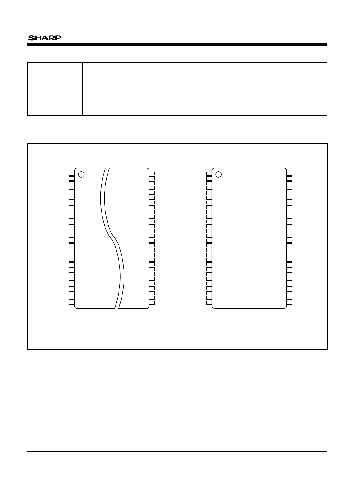
• Packages
– 56-pin TSOP Type I (TSOP056-P-1420)
Normal bend/Reverse bend
– 56-pin SSOP (SSOP056-P-0600)
★
[LH28F160S5-L]
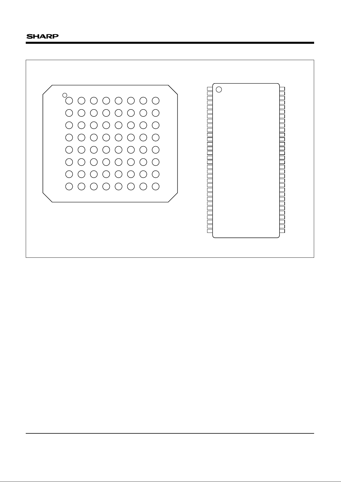
– 64-ball CSP (FBGA064-P-0811)
– 64-pin SDIP (SDIP064-P-0750)
★
∗ ETOX is a trademark of Intel Corporation.
★ Under development
LH28F160S5-L/S5H-L
16 M-bit (2 MB x 8/1 MB x 16) Smart 5
Flash Memories (Fast Programming)
- 1 -
In the absence of confirmation by device specification sheets, SHARP takes no responsibility for any defects that may occur in equipment using any SHARP devices shown in catalogs, data books,
etc. Contact SHARP in order to obtain the latest device specification sheets before using any SHARP device.
LH28F160S5-L/S5H-L
- 2 -
PIN CONNECTIONS ★ Under development
56-PIN TSOP (Type I)
(TSOP056-P-1420)
NC
CE
1#
NC
A
20
A19
A18
A17
A16
VCC
A15
A14
A13
A12
CE0#
V
PP
RP#
A
11
A10
A9
A8
GND
A
7
A6
A5
A4
A3
A2
A1
1
2
3
4
5
6
7
8
9
10
11
12
13
14
15
16
17
18
19
20
21
22
23
24
25
26
27
28
56
55
54
53
52
51
50
49
48
47
46
45
44
43
42
41
40
39
38
37
36
35
34
33
32
31
30
29
WP#
WE#
OE#
STS
DQ
15
DQ7
DQ14
DQ6
GND
DQ
13
DQ5
DQ12
DQ4
VCC
GND
DQ
11
DQ3
DQ10
DQ2
VCC
DQ9
DQ1
DQ8
DQ0
A0
BYTE#
NC
NC
56-PIN SSOP★ [LH28F160S5-L]
(SSOP056-P-0600)
CE0#
A
12
A13
A14
A15
NC
CE
1#
NC
A
20
A19
A18
A17
A16
VCC
GND
DQ
6
DQ14
DQ7
DQ15
STS
OE#
WE#
WP#
DQ
13
DQ5
DQ12
DQ4
VCC
1
2
3
4
5
6
7
8
9
10
11
12
13
14
15
16
17
18
19
20
21
22
23
24
25
26
27
28
56
55
54
53
52
51
50
49
48
47
46
45
44
43
42
41
40
39
38
37
36
35
34
33
32
31
30
29
VPP
RP#
A
11
A10
A9
A1
A2
A3
A4
A5
A6
A7
GND
A
8
VCC
DQ9
DQ1
DQ8
DQ0
A0
BYTE#
NC
NC
DQ
2
DQ10
DQ3
DQ11
GND
TOP VIEW
NOTE :
Reverse bend available on request.
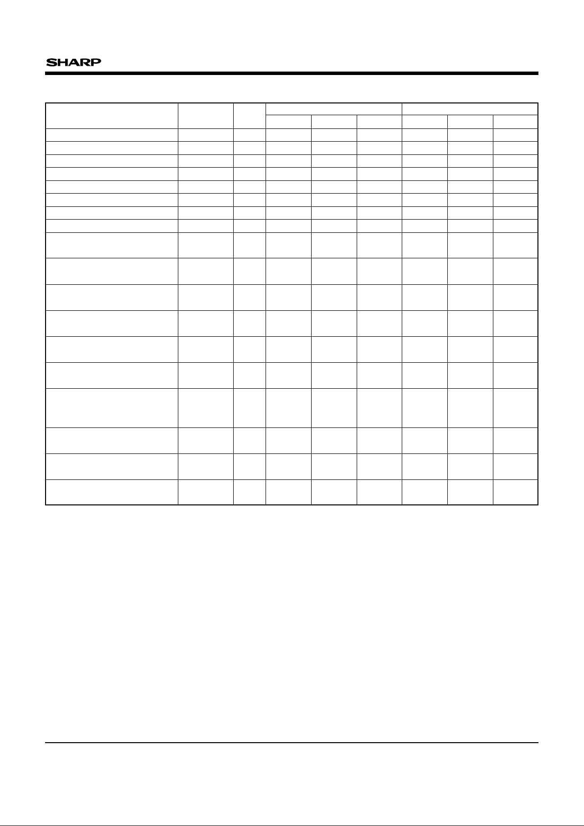
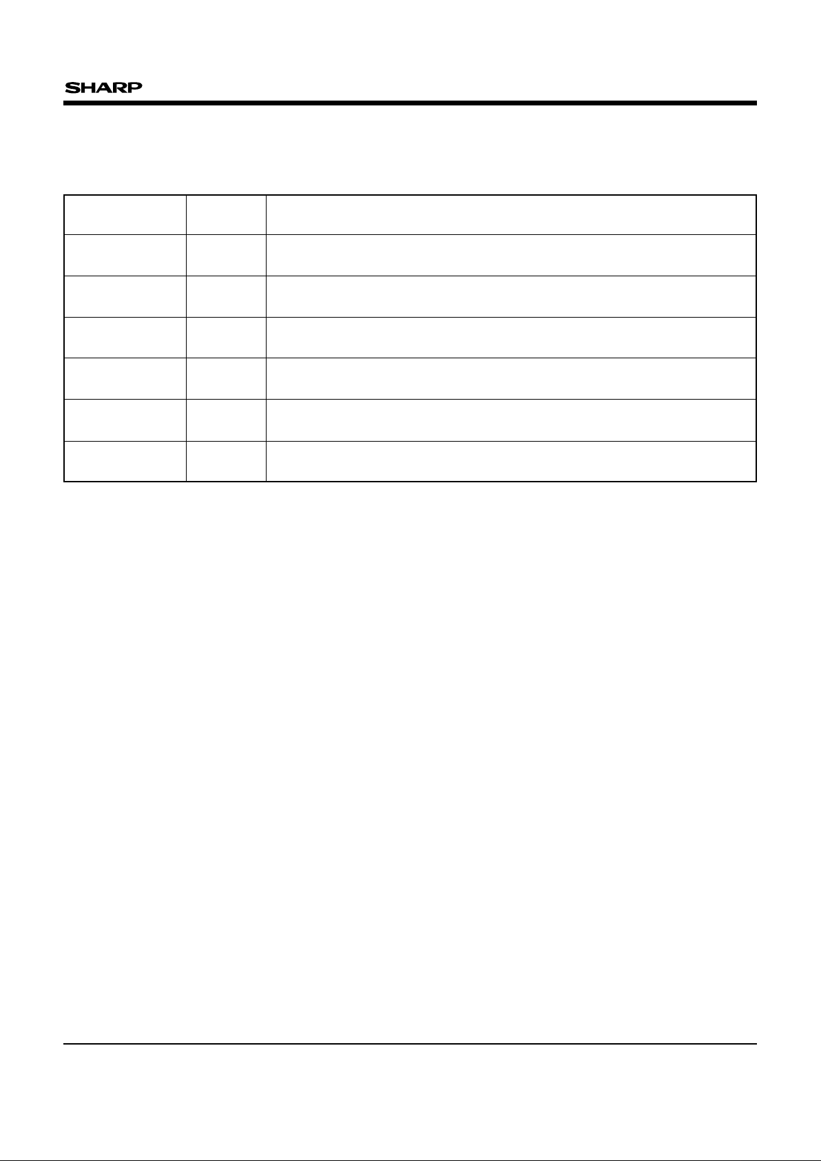
COMPARISON TABLE
VERSIONS
OPERATING
ACCESS TIME
DC CHARACTERISTICS
PACKAGE
TEMPERATURE
at 5.0±0.5 V
VCCdeep power-down current (MAX.)
LH28F160S5-L70/L10
0 to +70˚C 80 ns/100 ns 15 µA
56-pin TSOP (I), 56-pin SSOP
★
,
64-ball CSP, 64-pin SDIP
★
LH28F160S5H-L70/L10
–40 to +85˚C 90 ns/100 ns 20 µA
56-pin TSOP (I), 64-ball CSP,
64-pin SDIP
★
★ Under development
LH28F160S5-L/S5H-L
- 3 -
TOP VIEW
PIN CONNECTIONS (contd.) ★ Under development
64-PIN SDIP
★
(SDIP064-P-0750)
VPP
RP#
A
11
A10
A9
A8
GND
A7
A6
A5
A4
A3
A2
A1
NC
NC
NC
NC
NC
NC
NC
BYTE#
A
0
DQ0
DQ8
DQ1
DQ9
VCC
DQ2
DQ10
DQ3
DQ11
1
2
3
4
5
6
7
8
9
10
11
12
13
14
15
16
17
18
19
20
21
22
23
24
25
26
27
28
29
30
31
32
64
63
62
61
60
59
58
57
56
55
54
53
52
51
50
49
48
47
46
45
44
43
42
41
40
39
38
37
36
35
34
33
CE0#
A
12
A13
A14
A15
VCC
A16
A17
A18
A19
A20
NC
CE
1#
NC
NC
NC
NC
WP#
WE#
OE#
STS
DQ
15
DQ7
DQ14
DQ6
GND
DQ
13
DQ5
DQ12
DQ4
VCC
GND
NC
1
A
A17
B
A15
C
A12
D
RP#
E
A
9
A20
2
A
18
VCC
CE0#
VPP
A8
NC NC
WP#
3
A14
A13
A11
A10
4
CE1#
NC
NC
GND
5
WE#
DQ6
NC
NC
DQ9
OE#
6
DQ15
DQ5
DQ12
DQ3
DQ10
STS
7
DQ7
GND
VCC
GND
VCC
NC
8
DQ14
DQ13
DQ4
DQ11
DQ2
F
A7G
NCA6A4A5A3A2A1
NCNCDQ0
BYTE#
DQ8A0DQ1
NC
H
A16
A19
(FBGA064-P-0811)
64-BALL CSP
LH28F160S5-L/S5H-L
- 4 -
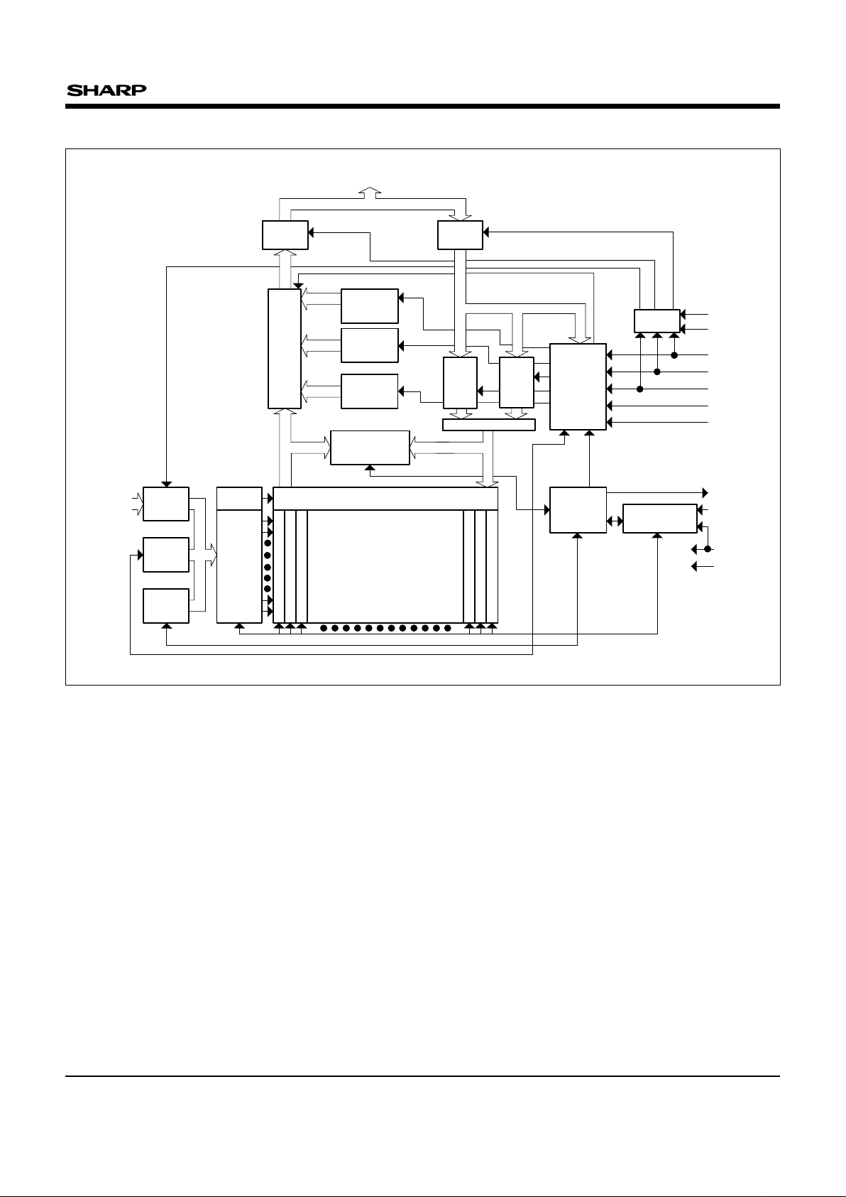
BLOCK DIAGRAM
OUTPUT
BUFFER
INPUT
BUFFER
I/O LOGIC
COMMAND
USER
INTERFACE
CE#
WE#
RP#
OE#
IDENTIFIER
REGISTER
STATUS
REGISTER
DATA
COMPARATOR
Y GATING
Y
DECODER
X
DECODER
32
64 k-BYTE
BLOCKS
INPUT
BUFFER
ADDRESS
LATCH
ADDRESS
COUNTER
WRITE STATE
MACHINE
PROGRAM/ERASE
VOLTAGE SWITCH
STS
GND
QUERY
ROM
DATA
REGISTER
WP#
BYTE#
MULTIPLEXER
PAGE
BUFFER
OUTPUT
MULTIPLEXER
VCC
VPP
VCC
A
0-A20
DQ0-DQ15
LH28F160S5-L/S5H-L
- 5 -
PIN DESCRIPTION
SYMBOL TYPE NAME AND FUNCTION
ADDRESS INPUTS : Inputs for addresses during read and write operations. Addresses
are internally latched during a write cycle.
A
0-A20 INPUT
A
0 : Byte Select Address. Not used in x16 mode (can be floated).
A
1-A4 : Column Address. Selects 1 of 16-bit lines.
A
5-A15 : Row Address. Selects 1 of 2 048-word lines.
A16-A20 : Block Address.
DATA INPUT/OUTPUTS :
DQ
0-DQ7 : Inputs data and commands during CUI write cycles; outputs data during
memory array, status register, query, and identifier code read cycles. Data pins float to
high-impedance when the chip is deselected or outputs are disabled. Data is internally
latched during a write cycle.
DQ
8-DQ15 : Inputs data during CUI write cycles in x16 mode; outputs data during memory
array read cycles in x16 mode; not used for statusregister, query and identifier code read
mode. Data pins float to high-impedance when the chip is deselected, outputs are
disabled, or in x8 mode (BYTE# = VIL). Data is internally latched during a write cycle.
CE
0#, CE1# INPUT
CHIP ENABLE : Activates the device’s control logic, input buffers decoders, and sense
amplifiers. Either CE
0# or CE1# VIH deselects the device and reduces power
consumption to standby levels. Both CE0# and CE1# must be VIL to select the devices.
RP# INPUT
RESET/DEEP POWER-DOWN : Puts the device in deep power-down mode and resets
internal automation. RP# V
IH enables normal operation. When driven VIL, RP# inhibits
write operations which provide data protection during power transitions. Exit from deep
power-down sets the device to read array mode.
OE# INPUT OUTPUT ENABLE : Gates the device’s outputs during a read cycle.
WE# INPUT
WRITE ENABLE : Controls writes to the CUI and array blocks. Addresses and data are
latched on the rising edge of the WE# pulse.
STS (RY/BY#) : Indicates the status of the internal WSM. When configured in level
mode (default mode), it acts as a RY/BY# pin. When low, the WSM is performing an
internal operation (block erase, full chip erase, (multi) word/byte write or block lock-bit
configuration). STS High Z indicates that the WSM is ready for new commands, block
erase is suspended, and (multi) word/byte write is inactive, (multi) word/byte write is
suspended or the device is in deep power-down mode. For alternate configurations of
the STATUS pin, see the Configuration command (Table 3 and Section 4.14).
WP# INPUT
WRITE PROTECT : Master control for block locking. When V
IL, locked blocks can not
be erased and programmed, and block lock-bits can not be set and reset.
BYTE# INPUT
BYTE ENABLE : BYTE# V
IL places device in x8 mode. All data are then input or output
on DQ
0-7, and DQ8-15 float. BYTE# VIH places the device in x16 mode, and turns off the
A0 input buffer.
BLOCK ERASE, FULL CHIP ERASE, (MULTI) WORD/BYTE WRITE, BLOCK LOCKBIT CONFIGURATION POWER SUPPLY : For erasing array blocks, writing bytes or
configuring block lock-bits. With V
PP
≤
V
PPLK, memory contents cannot be altered. Block
erase, full chip erase, (multi) word/byte write and block lock-bit configuration with an
invalid V
PP (see Section 6.2.3 "DC CHARACTERISTICS") produce spurious results
and should not be attempted.
V
CC SUPPLY
DEVICE POWER SUPPLY : Internal detection configures the device for 5 V operation.
Do not float any power pins. With V
CC
≤
V
LKO, all write attempts to the flash memory
are inhibited. Device operations at invalid V
CC voltage (see Section 6.2.3 "DC
CHARACTERISTICS") produce spurious results and should not be attempted.
GND SUPPLY GROUND : Do not float any ground pins.
NC NO CONNECT : Lead is not internal connected; recommend to be floated.
DQ0-DQ15
INPUT/
OUTPUT
OPEN
STS DRAIN
OUTPUT
V
PP SUPPLY
1 INTRODUCTION
This datasheet contains LH28F160S5-L/S5H-L
specifications. Section 1 provides a flash memory
overview. Sections 2, 3, 4, and 5 describe the
memory organization and functionality. Section 6
covers electrical specifications. LH28F160S5-L/
S5H-L flash memories documentation also includes
ordering information which is referenced in
Section 7.
1.1 Product Overview
The LH28F160S5-L/S5H-L are high-performance
16 M-bit Smart 5 flash memories organized as
2 MB x 8/1 MB x 16. The 2 MB of data is arranged
in thirty-two 64 k-byte blocks which are individually
erasable, lockable, and unlockable in-system. The
memory map is shown in Fig.1.
Smart 5 technology provides a choice of V
CC and
V
PP combination, as shown in Table 1, to meet
system performance and power expectations. V
PP
at 5 V eliminates the need for a separate 12 V
converter, while V
PP = 5 V maximizes erase and
write performance. In addition to flexible erase and
program voltages, the dedicated V
PP pin gives
complete data protection when V
PP ≤ VPPLK.
Table 1 VCC and VPP Voltage Combination
Offered by Smart 5 Technology
Internal VCC and VPP detection circuitry automatically configures the device for optimized read
and write operations.
A Command User Interface (CUI) serves as the
interface between the system processor and
internal operation of the device. A valid command
sequence written to the CUI initiates device
automation. An internal Write State Machine (WSM)
automatically executes the algorithms and timings
necessary for block erase, full chip erase, (multi)
word/byte write and block lock-bit configuration
operations.
A block erase operation erases one of the device’s
64 k-byte blocks typically within 0.34 second (5 V
V
CC, 5 V VPP) independent of other blocks. Each
block can be independently erased 100 000 times
(3.2 million block erases per device). Block erase
suspend mode allows system software to suspend
block erase to read data from, or write data to any
other block.
A word/byte write is performed in byte increments
typically within 9.24 µs (5 V V
CC, 5 V VPP). A multi
word/byte write has high speed write performance
of 2 µs/byte (5 V V
CC, 5 V VPP). (Multi) word/byte
write suspend mode enables the system to read
data from, or write data to any other flash memory
array location.
Individual block locking uses a combination of bits
and WP#, thirty-two block lock-bits, to lock and
unlock blocks. Block lock-bits gate block erase, full
chip erase and (multi) word/byte write operations.
Block lock-bit configuration operations (Set Block
Lock-Bit and Clear Block Lock-Bits commands) set
and cleared block lock-bits.
The status register indicates when the WSM’s block
erase, full chip erase, (multi) word/byte write or
block lock-bit configuration operation is finished.
The STS output gives an additional indicator of
WSM activity by providing both a hardware signal
of status (versus software polling) and status
masking (interrupt masking for background block
erase, for example). Status polling using STS
minimizes both CPU overhead and system power
consumption. STS pin can be configured to
different states using the Configuration command.
The STS pin defaults to RY/BY# operation. When
low, STS indicates that the WSM is performing a
VCC VOLTAGE VPP VOLTAGE
5 V 5 V
LH28F160S5-L/S5H-L
- 6 -
- 7 -
LH28F160S5-L/S5H-L
block erase, full chip erase, (multi) word/byte write
or block lock-bit configuration. STS High Z indicates
that the WSM is ready for a new command, block
erase is suspended and (multi) word/byte write are
inactive, (multi) word/byte write are suspended, or
the device is in deep power-down mode. The other
3 alternate configurations are all pulse mode for
use as a system interrupt.
The access time is 70 ns (t
AVQV) at the VCC supply
voltage range of 4.75 to 5.25 V over the temperature
range, 0 to +70°C (LH28F160S5-L)/
–40 to +85°C
(LH28F160S5H-L). At 4.5 to 5.5 V V
CC, the access
time is 80 ns/100 ns (LH28F160S5-L70/S5-L10) or
90 ns/100 ns (LH28F160S5H-L70/S5H-L10).
The Automatic Power Saving (APS) feature
substantially reduces active current when the
device is in static mode (addresses not switching).
In APS mode, the typical I
CCR current is 1 mA at
5 V V
CC.
When either CE
0# or CE1#, and RP# pins are at
V
CC, the ICC CMOS standby mode is enabled.
When the RP# pin is at GND, deep power-down
mode is enabled which minimizes power
consumption and provides write protection during
reset. A reset time (t
PHQV) is required from RP#
switching high until outputs are valid. Likewise, the
device has a wake time (t
PHEL) from RP#-high until
writes to the CUI are recognized. With RP# at
GND, the WSM is reset and the status register is
cleared.
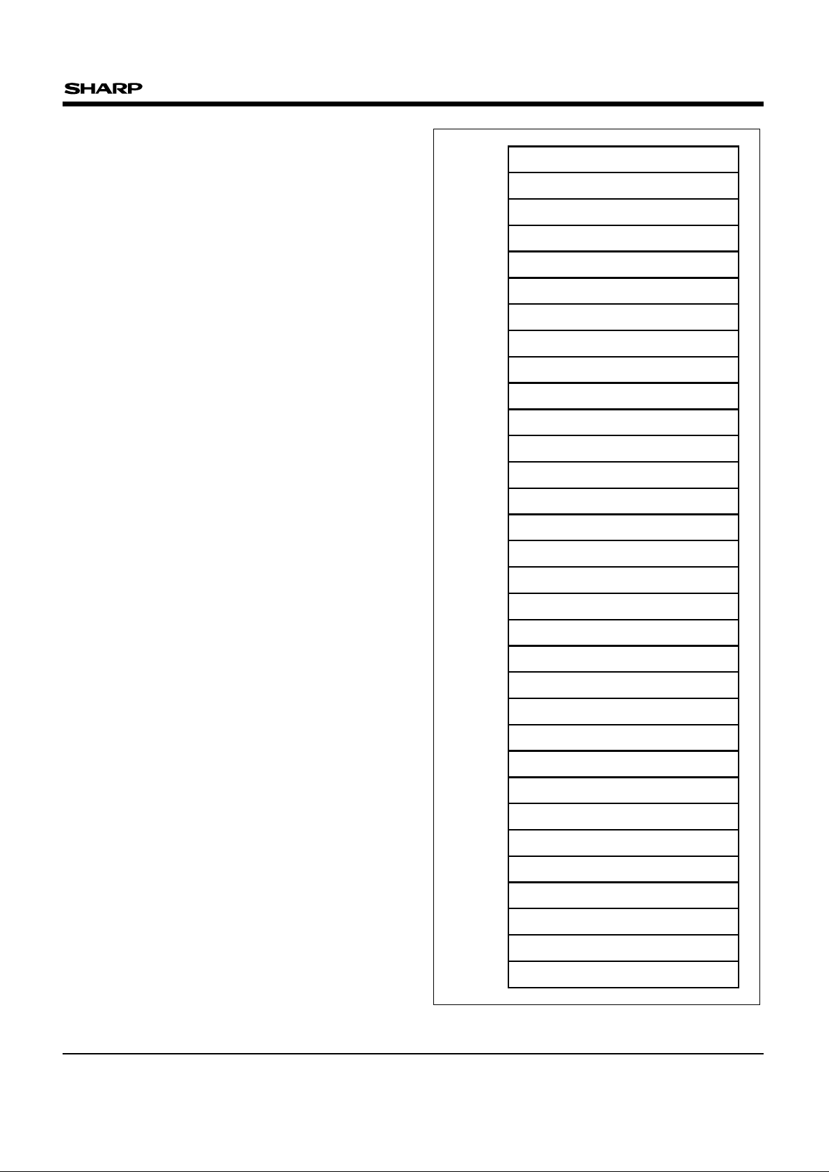
Fig. 1 Memory Map
64 k-Byte Block
64 k-Byte Block
64 k-Byte Block
64 k-Byte Block
64 k-Byte Block
64 k-Byte Block
64 k-Byte Block
64 k-Byte Block
64 k-Byte Block
64 k-Byte Block
64 k-Byte Block
64 k-Byte Block
64 k-Byte Block
64 k-Byte Block
64 k-Byte Block
64 k-Byte Block
64 k-Byte Block
64 k-Byte Block
64 k-Byte Block
64 k-Byte Block
64 k-Byte Block
64 k-Byte Block
64 k-Byte Block
64 k-Byte Block
64 k-Byte Block
64 k-Byte Block
64 k-Byte Block
64 k-Byte Block
64 k-Byte Block
64 k-Byte Block
64 k-Byte Block
64 k-Byte Block
1FFFFF
1F0000
1EFFFF
1E0000
1DFFFF
1D0000
1CFFFF
1C0000
1BFFFF
1B0000
1AFFFF
1A0000
19FFFF
190000
18FFFF
180000
17FFFF
170000
16FFFF
160000
15FFFF
150000
14FFFF
140000
13FFFF
130000
12FFFF
120000
11FFFF
110000
10FFFF
100000
0FFFFF
0F0000
0EFFFF
0E0000
0DFFFF
0D0000
0CFFFF
0C0000
0BFFFF
0B0000
0AFFFF
0A0000
09FFFF
090000
08FFFF
080000
07FFFF
070000
06FFFF
060000
05FFFF
050000
04FFFF
040000
03FFFF
030000
02FFFF
020000
01FFFF
010000
00FFFF
000000
31
30
29
28
27
26
25
24
23
22
21
20
19
18
17
16
15
14
13
12
11
10
9
8
7
6
5
4
3
2
1
0

2 PRINCIPLES OF OPERATION
The LH28F160S5-L/S5H-L flash memories include
an on-chip WSM to manage block erase, full chip
erase, (multi) word/byte write and block lock-bit
configuration functions. It allows for : 100% TTLlevel control inputs, fixed power supplies during
block erase, full chip erase, (multi) word/byte write
and block lock-bit configuration, and minimal
processor overhead with RAM-like interface timings.
After initial device power-up or return from deep
power-down mode (see Table 2.1 and Table 2.2
"Bus Operations"), the device defaults to read
array mode. Manipulation of external memory
control pins allow array read, standby, and output
disable operations.
Status register, query structure and identifier codes
can be accessed through the CUI independent of
the V
PP voltage. High voltage on VPP enables
successful block erase, full chip erase, (multi)
word/byte write and block lock-bit configuration. All
functions associated with altering memory
contents—block erase, full chip erase, (multi)
word/byte write and block lock-bit configuration,
status, query and identifier codes—are accessed
via the CUI and verified through the status register.
Commands are written using standard microprocessor write timings. The CUI contents serve as
input to the WSM, which controls the block erase,
full chip erase, (multi) word/byte write and block
lock-bit configuration. The internal algorithms are
regulated by the WSM, including pulse repetition,
internal verification, and margining of data.
Addresses and data are internally latched during
write cycles. Writing the appropriate command
outputs array data, accesses the identifier codes,
outputs query structure or outputs status register
data.
Interface software that initiates and polls progress
of block erase, full chip erase, (multi) word/byte
write and block lock-bit configuration can be stored
in any block. This code is copied to and executed
from system RAM during flash memory updates.
After successful completion, reads are again
possible via the Read Array command. Block erase
suspend allows system software to suspend a
block erase to read/write data from/to blocks other
than that which is suspended. Write suspend allows
system software to suspend a (multi) word/byte
write to read data from any other flash memory
array location.
2.1 Data Protection
Depending on the application, the system designer
may choose to make the V
PP power supply
switchable (available only when block erase, full
chip erase, (multi) word/byte write and block lock-bit
configuration are required) or hardwired to V
PPH1.
The device accommodates either design practice
and encourages optimization of the processormemory interface.
When V
PP ≤ VPPLK, memory contents cannot be
altered. The CUI, with multi-step block erase, full
chip erase, (multi) word/byte write and block lock-bit
configuration command sequences, provides
protection from unwanted operations even when
high voltage is applied to V
PP. All write functions
are disabled when V
CC is below the write lockout
voltage V
LKO or when RP# is at VIL. The device’s
block locking capability provides additional
protection from inadvertent code or data alteration
by gating block erase, full chip erase and (multi)
word/byte write operations.
LH28F160S5-L/S5H-L
- 8 -

3 BUS OPERATION
The local CPU reads and writes flash memory insystem. All bus cycles to or from the flash memory
conform to standard microprocessor bus cycles.
3.1 Read
Information can be read from any block, identifier
codes, query structure, or status register
independent of the V
PP voltage. RP# must be at
V
IH.
The first task is to write the appropriate read mode
command (Read Array, Read Identifier Codes,
Query or Read Status Register) to the CUI. Upon
initial device power-up or after exit from deep
power-down mode, the device automatically resets
to read array mode. Five control pins dictate the
data flow in and out of the component : CE#
(CE
0#, CE1#), OE#, WE#, RP# and WP#. CE0#,
CE
1# and OE# must be driven active to obtain data
at the outputs. CE
0# and CE1# are the device
selection control, and when active enables the
selected memory device. OE# is the data output
(DQ
0-DQ15) control and when active drives the
selected memory data onto the I/O bus. WE# and
RP# must be at V
IH. Fig. 15 and Fig. 16, illustrate
a read cycle.
3.2 Output Disable
With OE# at a logic-high level (VIH), the device
outputs are disabled. Output pins DQ
0-DQ15 are
placed in a high-impedance state.
3.3 Standby
Either CE0# or CE1# at a logic-high level (VIH)
places the device in standby mode which
substantially reduces device power consumption.
DQ
0-DQ15 outputs are placed in a high-impedance
state independent of OE#. If deselected during
block erase, full chip erase, (multi) word/byte write
and block lock-bit configuration, the device
continues functioning, and consuming active power
until the operation completes.
3.4 Deep Power-Down
RP# at VIL initiates the deep power-down mode.
In read modes, RP#-low deselects the memory,
places output drivers in a high-impedance state and
turns off all internal circuits. RP# must be held low
for a minimum of 100 ns. Time t
PHQV is required
after return from power-down until initial memory
access outputs are valid. After this wake-up
interval, normal operation is restored. The CUI is
reset to read array mode and status register is set
to 80H.
During block erase, full chip erase, (multi) word/byte
write or block lock-bit configuration modes, RP#-low
will abort the operation. STS remains low until the
reset operation is complete. Memory contents being
altered are no longer valid; the data may be
partially erased or written. Time t
PHWL is required
after RP# goes to logic-high (V
IH) before another
command can be written.
As with any automated device, it is important to
assert RP# during system reset. When the system
comes out of reset, it expects to read from the flash
memory. Automated flash memories provide status
information when accessed during block erase, full
chip erase, (multi) word/byte write and block lock-bit
configuration. If a CPU reset occurs with no flash
memory reset, proper CPU initialization may not
occur because the flash memory may be providing
status information instead of array data. SHARP’s
flash memories allow proper CPU initialization
following a system reset through the use of the
RP# input. In this application, RP# is controlled by
the same RESET# signal that resets the system
CPU.
LH28F160S5-L/S5H-L
- 9 -
- 10 -
LH28F160S5-L/S5H-L
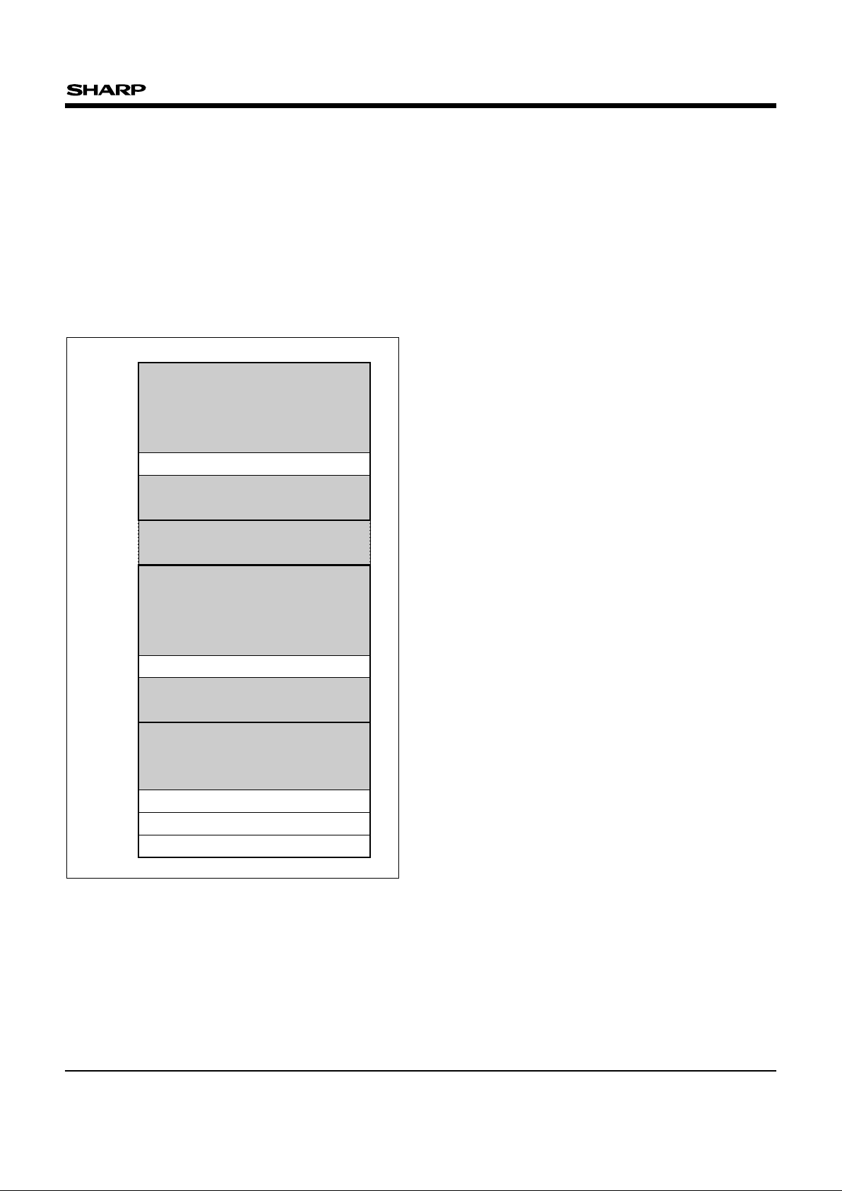
3.5 Read Identifier Codes Operation
The read identifier codes operation outputs the
manufacture code, device code, block status codes
for each block (see Fig. 2). Using the manufacture
and device codes, the system CPU can
automatically match the device with its proper
algorithms. The block status codes identify locked
or unlocked block setting and erase completed or
erase uncompleted condition.
Fig. 2 Device Identifier Code Memory Map
3.6 Query Operation
The query operation outputs the query structure.
Query database is stored in the 48-byte ROM.
Query structure allows system software to gain
critical information for controlling the flash
component. Query structures are always presented
on the lowest-order data output (DQ
0-DQ7) only.
3.7 Write
Writing commands to the CUI enable reading of
device data and identifier codes. They also control
inspection and clearing of the status register. When
V
CC = VCC1/2 and V PP = VPPH1, the CUI additionally
controls block erase, full chip erase, (multi)
word/byte write and block lock-bit configuration.
The Block Erase command requires appropriate
command data and an address within the block to
be erased. The Word/Byte Write command requires
the command and address of the location to be
written. Set Block Lock-Bit command requires the
command and block address within the device
(Block Lock) to be locked. The Clear Block LockBits command requires the command and address
within the device.
The CUI does not occupy an addressable memory
location. It is written when WE# and CE# are
active. The address and data needed to execute a
command are latched on the rising edge of WE# or
CE# (whichever goes high first). Standard
microprocessor write timings are used. Fig. 17 and
Fig. 18 illustrate WE# and CE#-controlled write
operations.
4 COMMAND DEFINITIONS
When the VPP voltage ≤ VPPLK, read operations
from the status register, identifier codes, query, or
blocks are enabled. Placing V
PPH1 on VPP enables
successful block erase, full chip erase, (multi)
word/byte write and block lock-bit configuration
operations.
Device operations are selected by writing specific
commands into the CUI. Table 3 defines these
commands.
1FFFFF
1F0006
1F0005
1F0004
1F0003
1F0000
1EFFFF
020000
01FFFF
010006
010005
010004
010003
010000
00FFFF
000006
000005
000004
000003
000002
000001
000000
Reserved for
Future Implementation
Block 31 Status Code
Block 31
Block 1
Block 0
(Blocks 2 through 30)
Reserved for
Future Implementation
Reserved for
Future Implementation
Block 1 Status Code
Reserved for
Future Implementation
Reserved for
Future Implementation
Block 0 Status Code
Device Code
Manufacture Code
- 11 -
LH28F160S5-L/S5H-L
Table 2.1 Bus Operations (BYTE# = VIH)
MODE NOTE RP# CE0#CE1# OE# WE#
ADDRESS
VPP DQ0-15 STS
Read
1, 2, 3, 9
VIH VIL VIL VIL VIH XXDOUT X
Output Disable 3 VIH VIL VIL VIH VIH X X High Z X
V
IH VIH
Standby 3 VIH VIH VIL X X X X High Z X
VIL VIH
Deep Power-Down 4 VIL X X X X X X High Z High Z
Read Identifier
9V
IH VIL VIL VIL VIH
See
X(
NOTE 5)
High Z
Codes
Fig. 2
Query 9 V
IH VIL VIL VIL VIH
See Table
X(
NOTE 6)
High Z
6 through 10
Write
3, 7, 8, 9
VIH VIL VIL VIH VIL XXDIN X
Table 2.2 Bus Operations (BYTE# = VIL)
MODE NOTE RP# CE0#CE1# OE# WE#
ADDRESS
VPP DQ0-7 STS
Read
1, 2, 3, 9
VIH VIL VIL VIL VIH XXDOUT X
Output Disable 3 VIH VIL VIL VIH VIH X X High Z X
VIH VIH
Standby 3 VIH VIH VIL X X X X High Z X
VIL VIH
Deep Power-Down 4 VIL X X X X X X High Z High Z
Read Identifier
9V
IH VIL VIL VIL VIH
See
X
(NOTE 5)
High Z
Codes
Fig. 2
Query 9 V
IH VIL VIL VIL VIH
See Table
X
(NOTE 6)
High Z
6 through 10
Write
3, 7, 8, 9
VIH VIL VIL VIH VIL XXDIN X
NOTES :
1. Refer to Section 6.2.3 "DC CHARACTERISTICS".
When V
PP ≤ VPPLK, memory contents can be read, but
not altered.
2. X can be V
IL or VIH for control pins and addresses, and
V
PPLK or VPPH1 for VPP. See Section 6.2.3 "DC
CHARACTERISTICS
" for VPPLK and VPPH1 voltages.
3. STS is V
OL (if configured to RY/BY# mode) when the
WSM is executing internal block erase, full chip erase,
(multi) word/byte write or block lock-bit configuration
algorithms. It is floated during when the WSM is not
busy, in block erase suspend mode with (multi)
word/byte write inactive, (multi) word/byte write suspend
mode, or deep power-down mode.
4. RP# at GND±0.2 V ensures the lowest deep powerdown current.
5. See Section 4.2 for read identifier code data.
6. See Section 4.5 for query data.
7. Command writes involving block erase, full chip erase,
(multi) word/byte write or block lock-bit configuration are
reliably executed when V
PP = VPPH1 and VCC = VCC1/2.
8. Refer to Table 3 for valid D
IN during a write operation.
9. Don’t use the timing both OE# and WE# are V
IL.
LH28F160S5-L/S5H-L
- 12 -
Table 3 Command Definitions
(NOTE 10)
COMMAND
BUS CYCLES
NOTE
FIRST BUS CYCLE SECOND BUS CYCLE
REQ’D.
Oper
(NOTE 1)
Addr
(NOTE 2)
Data
(NOTE 3)
Oper
(NOTE 1)
Addr
(NOTE 2)
Data
(NOTE 3)
Read Array/Reset 1 Write X FFH
Read Identifier Codes ≥ 2 4 Write X 90H Read IA ID
Query ≥ 2 Write X 98H Read QA QD
Read Status Register 2 Write X 70H Read X SRD
Clear Status Register 1 Write X 50H
Block Erase Setup/Confirm 2 5 Write BA 20H Write BA D0H
Full Chip Erase Setup/Confirm
2 Write X 30H Write X D0H
Word/Byte Write Setup/Write 2 5, 6 Write WA 40H Write WA WD
Alternate Word/Byte Write
2 5, 6 Write WA 10H Write WA WD
Setup/Write
Multi Word/Byte Write
≥ 4 9 Write WA E8H Write WA N
–1
Setup/Confirm
Block Erase and (Multi)
1 5 Write X B0H
Word/Byte Write Suspend
Confirm and Block Erase and
1 5 Write X D0H
(Multi) Word/Byte Write Resume
Block Lock-Bit Set
2 7 Write BA 60H Write BA 01H
Setup/Confirm
Block Lock-Bit Reset
2 8 Write X 60H Write X D0H
Setup/Confirm
STS Configuration
Level-Mode for Erase 2 Write X B8H Write X 00H
and Write (RY/BY# Mode)
STS Configuration
2 Write X B8H Write X 01H
Pulse-Mode for Erase
STS Configuration
2 Write X B8H Write X 02H
Pulse-Mode for Write
STS Configuration Pulse-Mode
2 Write X B8H Write X 03H
for Erase and Write
NOTES :
1. Bus operations are defined in Table 2.1 and Table 2.2.
2. X = Any valid address within the device.
IA = Identifier code address : see Fig. 2.
QA = Query offset address.
BA = Address within the block being erased or locked.
WA = Address of memory location to be written.
3. SRD = Data read from status register. See Table 13.1
for a description of the status register bits.
WD = Data to be written at location WA. Data is latched
on the rising edge of WE# or CE# (whichever
goes high first).
ID = Data read from identifier codes.
QD = Data read from query database.
4. Following the Read Identifier Codes command, read
operations access manufacture, device and block status
codes. See Section 4.2 for read identifier code data.
5. If the block is locked, WP# must be at V
IH to enable
block erase or (multi) word/byte write operations.
Attempts to issue a block erase or (multi) word/byte write
to a locked block while RP# is V
IH.
6. Either 40H or 10H is recognized by the WSM as the
byte write setup.
7. A block lock-bit can be set while WP# is V
IH.
8. WP# must be at V
IH to clear block lock-bits. The clear
block lock-bits operation simultaneously clears all block
lock-bits.
9. Following the Third Bus Cycle, inputs the write address
and write data of "N" times. Finally, input the confirm
command "D0H".
10. Commands other than those shown above are reserved
by SHARP for future device implementations and should
not be used.
- 13 -
LH28F160S5-L/S5H-L
4.1 Read Array Command
Upon initial device power-up and after exit from
deep power-down mode, the device defaults to
read array mode. This operation is also initiated by
writing the Read Array command. The device
remains enabled for reads until another command
is written. Once the internal WSM has started a
block erase, full chip erase, (multi) word/byte write
or block lock-bit configuration, the device will not
recognize the Read Array command until the WSM
completes its operation unless the WSM is
suspended via an Erase Suspend and (Multi)
Word/Byte Write Suspend command. The Read
Array command functions independently of the V
PP
voltage and RP# must be VIH.
4.2 Read Identifier Codes Command
The identifier code operation is initiated by writing
the Read Identifier Codes command. Following the
command write, read cycles from addresses shown
in Fig. 2 retrieve the manufacture, device, block
lock configuration and block erase status (see
Table 4 for identifier code values). To terminate the
operation, write another valid command. Like the
Read Array command, the Read Identifier Codes
command functions independently of the V
PP
voltage and RP# must be VIH. Following the Read
Identifier Codes command, the following information
can be read :
Table 4 Identifier Codes
NOTE :
1. X selects the specific block status code to be read. See
Fig. 2 for the device identifier code memory map.
4.3 Read Status Register Command
The status register may be read to determine when
a block erase, full chip erase, (multi) word/byte
write or block lock-bit configuration is complete and
whether the operation completed successfully (see
Table 13.1). It may be read at any time by writing
the Read Status Register command. After writing
this command, all subsequent read operations
output data from the status register until another
valid command is written. The status register
contents are latched on the falling edge of OE# or
CE# (Either CE
0# or CE1#), whichever occurs. OE#
or CE# (Either CE
0# or CE1#) must toggle to VIH
before further reads to update the status register
latch. The Read Status Register command
functions independently of the V
PP voltage. RP#
must be V
IH.
The extended status register may be read to
determine multi byte write availability (see Table
13.2). The extended status register may be read at
any time by writing the Multi Byte Write command.
After writing this command, all subsequent read
operations output data from the extended status
register, until another valid command is written. The
contents of the extended status register are latched
on the falling edge of OE# or CE# (Either CE
0# or
CE
1#), whichever occurs last in the read cycle.
Multi Byte Write command must be re-issued to
update the extended status register latch.
4.4 Clear Status Register Command
Status register bits SR.5, SR.4, SR.3 and SR.1 are
set to "1"s by the WSM and can only be reset by
the Clear Status Register command. These bits
indicate various failure conditions (see Table 13.1).
By allowing system software to reset these bits,
several operations (such as cumulatively erasing or
locking multiple blocks or writing several bytes in
CODE ADDRESS DATA
Manufacture Code
00000H
B0
00001H
Device Code
00002H
D0
00003H
Block Status Code
X0004H
(NOTE 1)
X0005H
(NOTE 1)
•
Block is Unlocked DQ
0 = 0
•
Block is Locked DQ
0 = 1
•
Last erase operation
completed successfully
DQ
1 = 0
•
Last erase operation did
DQ
1 = 1
not completed successfully
•Reserved for Future Use DQ
2-7
LH28F160S5-L/S5H-L
- 14 -
sequence) may be performed. The status register
may be polled to determine if an error occurs
during the sequence.
To clear the status register, the Clear Status
Register command (50H) is written. It functions
independently of the applied V
PP voltage. RP#
must be V
IH. This command is not functional during
block erase, full chip erase, (multi) word/byte write,
block lock-bit configuration, block erase suspend or
(multi) word/byte write suspend modes.
4.5 Query Command
Query database can be read by writing Query
command (98H). Following the command write,
read cycle from address shown in Table 6 through
Table 10 retrieve the critical information to write,
erase and otherwise control the flash component.
A
0 of query offset address is ignored when x8
mode (BYTE# = V
IL).
Query data are always presented on the low-byte
data output (DQ
0-DQ7). In x16 mode, high-byte
(DQ
8-DQ15) outputs 00H. The bytes not assigned
to any information or reserved for future use are set
to "0". This command functions independently of
the V
PP voltage. RP# must be VIH.
Table 5 Example of Query Structure Output
4.5.1 BLOCK STATUS REGISTER
This field provides lock configuration and erase
status for the specified block. These informations
are only available when device is ready (SR.7 = 1).
If block erase or full chip erase operation is finished
irregularly, block erase status bit will be set to "1". If
bit 1 is "1", this block is invalid.
MODE OFFSET ADDRESS
OUTPUT
DQ15-8 DQ7-0
A5, A4, A3, A2, A1, A0
1, 0, 0, 0, 0, 0 (20H) High Z "Q"
x8 mode 1, 0, 0, 0, 0, 1 (21H) High Z "Q"
1, 0, 0, 0, 1, 0 (22H) High Z "R"
1, 0, 0, 0, 1, 1 (23H) High Z "R"
A5, A4, A3, A2, A1
x16 mode
1, 0, 0, 0, 0 (10H) 00H "Q"
1, 0, 0, 0, 1 (11H) 00H "R"
Table 6 Query Block Status Register
OFFSET
LENGTH DESCRIPTION
(Word Address)
(BA+2)H 01H Block Status Register
bit0 Block Lock Configuration
0 = Block is unlocked
1 = Block is locked
bit1 Block Erase Status
0 = Last erase operation completed successfully
1 = Last erase operation not completed successfully
bit2-7 Reserved for future use
NOTE :
BA = The beginning of a Block Address.
LH28F160S5-L/S5H-L
- 15 -
4.5.2 CFI QUERY IDENTIFICATION STRING
The identification string provides verification that the
component supports the Common Flash Interface
specification. Additionally, it indicates which version
of the spec and which vendor-specified command
set(s) is(are) supported.
Table 7 CFI Query Identification String
OFFSET
LENGTH DESCRIPTION
(Word Address)
10H, 11H, 12H 03H Query Unique ASCII string "QRY"
51H, 52H, 59H
13H, 14H 02H Primary Vendor Command Set and Control Interface ID Code
01H, 00H (SCS ID Code)
15H, 16H 02H Address for Primary Algorithm Extended Query Table
31H, 00H (SCS Extended Query Table Offset)
17H, 18H 02H Alternate Vendor Command Set and Control Interface ID Code
0000H (0000H means that no alternate exists)
19H, 1AH 02H Address for Alternate Algorithm Extended Query Table
0000H (0000H means that no alternate exists)
4.5.3 SYSTEM INTERFACE INFORMATION
The following device information can be useful in optimizing system interface software.
Table 8 System Information String
OFFSET
LENGTH DESCRIPTION
(Word Address)
1BH 01H V
CC Logic Supply Minimum Write/Erase voltage
27H (2.7 V)
1CH 01H V
CC Logic Supply Maximum Write/Erase voltage
55H (5.5 V)
1DH 01H V
PP Programming Supply Minimum Write/Erase voltage
27H (2.7 V)
1EH 01H V
PP Programming Supply Maximum Write/Erase voltage
55H (5.5 V)
1FH 01H Typical Time-Out per Single Byte/Word Write
03H (23= 8 µs)
20H 01H Typical Time-Out for Maximum Size Buffer Write (32 Bytes)
06H (26= 64 µs)
21H 01H Typical Time-Out per Individual Block Erase
0AH (0AH = 10, 210= 1 024 ms)
22H 01H Typical Time-Out for Full Chip Erase
0FH (0FH = 15, 215= 32 768 ms)
23H 01H Maximum Time-Out per Single Byte/Word Write, 2
N
times of typical.
04H (24= 16, 8 µs x 16 = 128 µs)
24H 01H Maximum Time-Out per Maximum Size Buffer Write, 2
N
times of typical.
04H (24= 16, 64 µs x 16 = 1 024 µs)
25H 01H Maximum Time-Out per Individual Block Erase, 2
N
times of typical.
04H (24= 16, 1 024 ms x 16 = 16 384 ms)
26H 01H Maximum Time-Out for Full Chip Erase, 2
N
times of typical.
04H (2
4
= 16, 32 768 ms x 16 = 524 288 ms)
LH28F160S5-L/S5H-L
4.5.4 DEVICE GEOMETRY DEFINITION
This field provides critical details of the flash device geometry.
Table 9 Device Geometry Definition
OFFSET
LENGTH DESCRIPTION
(Word Address)
27H 01H Device Size
15H (15H = 21, 221= 2 097 152 = 2 M Bytes)
28H, 29H 02H Flash Device Interface Description
02H, 00H (x8/x16 supports x8 and x16 via BYTE#)
2AH, 2BH 02H Maximum Number of Bytes in Multi Word/Byte Write
05H, 00H (25= 32 Bytes )
2CH 01H Number of Erase Block Regions within Device
01H (symmetrically blocked)
2DH, 2EH 02H The Number of Erase Blocks
1FH, 00H (1FH = 31 ⇒ 31 + 1 = 32 Blocks)
2FH, 30H 02H The Number of "256 Bytes" cluster in a Erase Block
00H, 01H (0100H = 256 ⇒ 256 Bytes x 256 = 64k Bytes in a Erase Block)
- 16 -
LH28F160S5-L/S5H-L
4.5.5 SCS OEM SPECIFIC EXTENDED QUERY
TABLE
Certain flash features and commands may be
optional in a vendor-specific algorithm specification.
The optional vendor-specific query table(s) may be
used to specify this and other types of information.
These structures are defined solely by the flash
vendor(s).
Table 10 SCS OEM Specific Extended Query Table
OFFSET
LENGTH DESCRIPTION
(Word Address)
31H, 32H, 33H 03H PRI
50H, 52H, 49H
34H 01H 31H (1) Major Version Number , ASCII
35H 01H 30H (0) Minor Version Number, ASCII
36H, 37H, 04H 0FH, 00H, 00H, 00H
38H, 39H Optional Command Support
bit0 = 1 : Chip Erase Supported
bit1 = 1 : Suspend Erase Supported
bit2 = 1 : Suspend Write Supported
bit3 = 1 : Lock/Unlock Supported
bit4 = 0 : Queued Erase Not Supported
bit5-31 = 0 : Reserved for future use
3AH 01H 01H
Supported Functions after Suspend
bit0 = 1 : Write Supported after Erase Suspend
bit1-7 = 0 : Reserved for future use
3BH, 3CH 02H 03H, 00H
Block Status Register Mask
bit0 = 1 : Block Status Register Lock Bit [BSR.0] active
bit1 = 1 : Block Status Register Valid Bit [BSR.1] active
bit2-15 = 0 : Reserved for future use
3DH 01H VCC Logic Supply Optimum Write/Erase voltage (highest performance)
50H (5.0 V)
3EH 01H
VPPProgramming Supply Optimum Write/Erase voltage (highest performance)
50H (5.0 V)
3FH reserved Reserved for future versions of the SCS specification
- 17 -
 Loading...